Implementation of Closed Loop Control of High Step up
Interleaved Converter with VoltageMultiplier Module and
Renewable Energy System
M.AVINASH M-tech Student Scholar
Department of Electrical & Electronics Engineering, Sri Venkateswara College of Engineering and Technology, Etcherla; Srikakulam (Dt); A.P, India.
M.SATISH KUMAR Assistant Professor
Department of Electrical & Electronics Engineering, Sri Venkateswara College of Engineering and Technology, Etcherla; Srikakulam (Dt); A.P, India. Abstract-- A High step-up converter suitable for
renewableenergy system is designed in this paper. Using a conventionalinterleaved boost converter, accompanied by a voltage multipliermodule composed of switched capacitors and coupled inductors,high step-up gain is obtained without operating at extreme dutyratio. The topology of the proposed converter reduces thecurrent stress. The topology constrains the input current ripple,and hence the conduction loss reduces. The circuit also increasesthe lifetime of the source. Because of the lossless passive clampperformance, the leakage energy can be recycled to the outputterminal. The low-voltage-rated MOSFETs can be adopted for reductions of conduction losses and cost. In addition, due to the lossless passive clamp performance, leakage energy is recycled to the output terminal.Hence, large voltage spikes across the main switches are alleviated, and the efficiency is improved. Closed loop control automatically maintains a precise output voltage regardless of variation in input voltage and load conditions.
Index Terms—RES, DC-DC Converter, high step-up converter, voltage multiplier module.
I.INTRODUCTION
Renewable energy being the best solution andemployed all over the world to satisfy the energy shortageexisting without environmental contamination[1]-[3].A mong the renewable energies available the mostpromising energy is Photovoltaic (PV) energy. Though PVsystem installation cost is high, it has lots of pros, as the systemis long lasting and maintenance frees [4]. No w-a-days, PVsystem has grasped the attention of the researchers, but highinstallation cost and low conversion efficiency are the majordrawbacks.
To extract maximu m power fro m the PV system MPPTtechnique can be implemented to the boost converters. Byadjusting the duty ratio of the converter, maximu m powerdelivered can be tracked by the PV panel. As the energygenerated by the PV system is not sufficient (i.e.) very lo wvoltage. IN order to overcome, the aforementioned cons in thePV system. The DC/DC boost converter is employed in betweenthe power generation stage and the load shown in the Fig.1. Thevoltage is boosted and high voltage is achieved.But, our conventional power converter has low efficiencydue to the poor conversion ratio. The semiconductor devices areused as the switch in the converter. Since, this switch
sufferswith voltage stress, the switching losses increases and efficiencyis decreased [5].
The proposed converter is the integration of voltagemultip lier module with the conventional interleaved boostconverter. Coupled inductors and switched capacitors togetherconstitute the voltage mu ltip lier module [6]. The design of thecoupled inductors can be used to extend step-up gain andhigher voltage conversion ratio is offered by the switchedcapacitors. Moreover, the energy stored in the magnetizinginductor will transfer v ia three respective paths when one ofthe switches turns off and thus current distribution decreases.Hence, the conduction losses decrease because of loweffective current. The currents through some diodes decreaseto zero before they turn off and hence diode reverse recoverylosses are also reduce. The objective of this paper is todevelop a converter with lo w switching losses, reducedvoltage and current stress and reduced conduction loss. Theleakage inductance of the isolation transformer, resulting inhigh voltage spike during switching transition is a major issue [7].The freewheeling current due to the leakage inductance willincrease the conduction losses and reduce the duty cycle. Anotable approach is to pre charge the leakage inductance andto raise its current level up to that of the current-fed inductor,thus reducing their current difference and voltage spikes. Asthe current level varies with variation in the load, it is difficultto tune the switching timing diagram to match these twocurrents [8].
because such a system requires a sufficientlyh igh up conversion with h igh efficiency. Conventional step-up converters, such as the boost converter and flyback converter, cannot achieve a high step-up conversion with high efficiency because of the resistances of elements or leakage inductance;also the voltage stresses are large [10].
Fig.1.Block diagram of renewable energy system The proposed converter is a conventional interleaved boost converter integrated with a voltage multiplier module, and the voltage multip lier module is composed of switched capacitors and coupled inductors. The coupled inductors can be designed to extend step-up gain, and the switched capacitors offer extra voltage conversion ratio. In addition, when one of the switches turns off, the energy stored in the magnetizing inductor will transfer via three respective paths; thus, the current distribution not only decreases the conduction losses by lower effective current but also makes currents through some diodes decrease to zero before they turn off, which alleviate diode reverse recovery losses.
II. CLOSED LOOP GRID CONNECTED SYSTEMS
DC motors are used extensively in ad justable speeddrives and position control applications. Their speeds lowerthe base speeds can be controlled by armature – voltagecontrol. Speeds over the base speed are obtained by field-flu xcontrol method. As speed control method for DC motors aresimp ler and less expensive than those for AC motors, DCmotors are preferred where wide speed range control isrequired. For this control objective of DC drive is obtained byusing power electronic device fed renewable energygeneration scheme now imp lemented in many industrialapplications. Fig. 2 shows the schematic diagram that the PVpanel is connected to the DC motor through proposedconverter by a closed loop control. In recent years, there hasbeen an upsurge of interest in solar photovoltaic (PV) energysystems in both industry and academia [7]. In typical PVpower generation
systems, several PV panels are connected inseries and parallel to form an array and feed energy to a singlecentralized converter [8]. An alternative approach is to use aDC module, which is a co mbination of one PV panel and onepower conditioning unit, to feed power directly into the DC load [9].
Fig.2.General Schematic of standalone system with closed loop control and grid connected systems.
A DC– DC converter with a high step-up voltage gain isused for several applications, such as high-intensity dischargelamp ballasts for automobile headlamps, fuel cell energyconversion systems, solar-cell energy conversion systems andbattery backup systems for uninterruptible power supplies.Theoretically, a dc–dc boost converter can achieve a highstep-up voltage gain with an extremely high duty ratio.However, in practice, the step-up voltage gain is limited dueto the effect of power switches, rectifier diodes and theequivalent series resistance (ESR) [10] of inductors andcapacitors.
III. OPERATING PRINCIPLES
Fig.3. Proposed high step-up converter.
The DC-DC converter requires large step-up voltage conversion fro m low voltage obtained fro m the panel to the required voltage level for the application. The previous research on various converters for high step-up applications has included analyses of the switched – capacitor type, the voltage-lift type, the capacitor-diode voltage mu ltiplier type and the boost type integrated with coupled inductor, these converters by increasing turns ratio of coupled inductor obtain higher voltage gain than conventional boost converter. So me converters successfully co mbined boost and fly back converters, since various converter combinations are developed to carryout high step up voltage gain by using the coupled-inductor technique. The efficiency and voltage gain of the DC-DC boost converter are constrained by either switches or the reverse recovery issues of the diodes.
At t = t0, the power switch S2 remains inON state, and the other power switch S1 begins to turn on. Thediodes
Dc1, Dc2, Db1, Db2, and Df1 are reversed biased. The
series leakage inductors Ls quicklyrelease the stored energy to the output terminal v ia flyback–fo rward diode Df2, and the current through series leakageinductors Ls decreases to zero. Thus, the magnetizing inductorLm1
still transfers energy to the secondary side of coupledinductors. The current through leakage inductor Lk1 increaseslinearly and the other current through
leakage inductor Lk2decreases linearly.At t = t1, both of
the power switches S1and S2 remain in ON state, and all diodes are reversed biased. Both currents through leakage inductorsLk1 and Lk2 are increased linearly due
to charging by inputvoltage source Vin.At t = t2, the
power switch S1 remainsin ONstate, and the other power switch S2 begins to turn off.The diodes Dc1, Db1, and Df2
are reversed biased. The energy stored in magnetizing inductor Lm2transfers to the secondary side of coupled
inductors, and the other modes of operations are presented in the simulation cases.
IV. STEADY-STATE ANALYSIS
The transient characteristics of circuitry are disregardedto simplify the circuit performance analysis of the proposedconverter in CCM , and some formu lated assumptions are asfollows.1) All of the components in the proposed converter are ideal.2) Leakage inductors Lk1, Lk2, and Ls are neglected.3) Vo ltages on all
capacitors are considered to be constantbecause of infinitely large capacitance.4) Due to the completely symmetrical interleaved structure,the related components are defined as the correspondingsymbols such as Dc1 and Dc2 defined as Dc.
A.Step-Up Gain
The voltage on clamp capacitor Cc can be regarded as anoutput voltage of the boost converter; thus, voltage VCccan bederived from
𝑉
𝐶𝐶=
11−𝐷
𝑉
𝑖𝑛(1)
When one of the switches turns off, voltage VC1 can obtain adouble output voltage of the boost converter derived from
𝑉𝐶1 = 1
1−𝐷𝑉𝑖𝑛+ 𝑉𝐶𝐶 = 2
1−𝐷𝑉𝑖𝑛 (2)
The output filter capacitors C2 and C3 are charged by energytransformation fro m the primary side. When S2 is in ON stateand S1 is in OFF state, VC2 is equal to the induced voltage ofNs1 plus the induced voltage of Ns2, and when S1 is in ON stateand S2 is in OFF state, VC3 is also equal to the induced voltageof Ns1 plus the induced voltage of Ns2. Thus, voltages VC2 andVC3 can be derived from
𝑉
𝐶2= 𝑉
𝐶3= 𝑛. 𝑉
𝑖𝑛(1 +
𝐷1+𝐷
) =
𝑛
1−𝐷
𝑉
𝑖𝑛 (3)The output voltage can be derived from
𝑉
𝑜= 𝑉
𝐶1+ 𝑉
𝐶2+ 𝑉
𝐶3=
2𝑛+21−𝐷
𝑉
𝑖𝑛 (4) In addition, the voltage gain o f the p roposed converter is𝑉𝑜
𝑉𝑖𝑛
=
2𝑛+2
1−𝐷 (5)
Fig. 4.Voltage gain versus turn ratio n and duty cycle.
B. Voltage Stress on Semiconductor Component
The voltage ripples on the capacitors are ignored to simp lifythe voltage stress analysis of the components of the proposedconverter. The voltage stress on power switch S is clamped and derived from-
𝑉
𝑆1= 𝑉
𝑆2=
2 1−𝐷𝑉
𝑖𝑛=
1
2𝑛+2
𝑉
𝑜(6)
Equation (6) confirms that low-voltage-rated MOSFET withlo w RDS(ON) can be adopted for the proposed converter toreduce conduction losses and costs. The voltage stress on thepower switch S accounts for a fourth of output voltage Vo, evenif turn ratio n is one. This feature makes the proposed convertersuitable for high step-up and high-power applications.
The voltage stress on diode Dc is equal to VC1, and thevoltage stress on diode Db is voltage VC1 minus voltage VCc.These voltage stresses can be derived from
𝑉
𝐷𝑐1= 𝑉
𝐷𝑐2=
2 1−𝐷
𝑉
𝑖𝑛=
1 𝑛+1
𝑉
𝑜(7)
𝑉
𝐷𝑏1= 𝑉
𝐷𝑏2= 𝑉
𝐶1− 𝑉
𝐶2=
1
1 − 𝐷
𝑉
𝑖𝑛(8)
The voltage stress on diode Db is close to the voltage stresson power switch S. Although the voltage stress on diode Dc islarger, it accounts for only half of output voltage Vo at a turnratio n of one. The voltage stresses on the diodes are lower asthe voltage gain is extended by increasing turn ratio n.The voltage stress on diode Df equals the VC2 plus VC3,which can be derived from
𝑉
𝐷𝑓1= 𝑉
𝐷𝑓1= 2𝑛 1−𝐷𝑉
𝑖𝑛=
𝑛 𝑛+1
𝑉
𝑜 (9)Although the voltage stress on the diode Df increases as theturn ratio n increases, the voltage stress on the diodes Df isalways lower than the output voltage.
V.SIMULATION RESULTS
Here the simulation is carried out by two different cases they are 1) high step-up interleaved converter with voltage multip lier module 2) closed-loop control of interleaved converter with voltage multiplier module
Case-1High step-up interleaved converter with voltage multiplier module
Fig.5.Simulink model of high step-up interleaved converter with voltage multiplier module
Fig.5 shows the simulin k model o f proposed converter operating in continuous conduction mode and the duty cycles of the power switches during steady operation are greater than 0.5 and are interleaved with a 180◦
phase shift. Fig.6& 7 shows the gating pulse to power switches S1 and S2. The other plot shows the voltage across the power switches S1 and S2. Fig.8 shows the voltage stresses on clamp diodes Dc1 and Dc2. These voltage stresses are doubles of voltage stresses on power switches S1 and S2. Fig.9 shows the output voltage of the high step-up interleaved converter with voltage multiplier module.
Fig.7.Power switch S2 gating pulse and output voltage
Fig.8.Voltage stresses onclamp diodes.
Fig.9. OutputVoltage of High Step-Up Interleaved ConverterWith Voltage Multiplier Module.
Case-2Closed-loop control of interleaved converter with voltage multiplier module
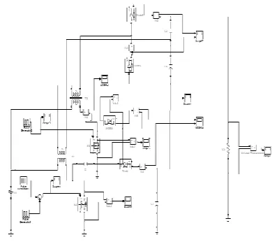
Fig.10Simulink Model Of Closed LoopControl Of Interleaved Converter With Voltage Multiplier Module.
Fig.11. Gating pulse of power switches S1 and S2.
Fig.12. Output Voltage of Closed LoopControl OfInterleaved Converter WithVoltage Multiplier Module.
switches S1 and S2. Fig.12 shows the output voltage of closed loop control of interleaved converter with voltage multiplier module.
VI. CONCLUS ION
This paper has presented the theoretical analysis of steady state, related consideration, simu lation results, for the proposed converter. The proposed converter has successfully implemented an efficienthigh step-up con- version through the voltage multiplier module. The interleaved structure reduces the input current ripple and distributes the cur- rent through each component. The proposed converterhas successfully implemented an efficient high step-up conversionthrough the voltage mu ltip lier module with high efficiency. Leakage energy is recycled and voltage spikes are constrained. Voltage stress on power switch is also lower than output voltage. The closed loop control automatically maintains a precise output voltage regardless of variation in input voltage and load conditions . These all simu lation results are tested and verified by using MATLAB/SIMULINK software.
REFERENCES
[1] J. T. Bialasiewicz, “Renewable energy systems with photovoltaic power generators: Operation and modeling,”IEEE Trans. Ind. Electron., vol. 55, no. 7, pp. 2752–2758, Jul. 2008.
[2] Y. P. Hsieh, J. F. Chen, T. J. Liang, and L. S. Yang, “Novel high stepup DC–DC converter with coupled-inductor and switched-capacitor techniques for a sustainable energy system,”IEEE Trans. Power Electron., vol. 26, no. 12, pp. 3481–3490, Dec. 2011.
[3] Q. Zhao and F. C. Lee, “High-efficiency, high step-up DC–DC converters,”IEEE Trans. Power Electron., vol. 18, no. 1, pp. 65–73, Jan. 2003.
[4] R. J. Wai, C. Y. Lin, R. Y. Duan, and Y. R. Chang, “High-efficiency DC–DC converter with high voltage gain and reduced switch stress,” IEEE Trans. Ind. Electron., vol. 54, no. 1, pp. 354–364, Feb. 2007.
[5] Y. Jang and M. M. Jovanovic, “Interleaved boost converter with intrinsic voltage-doubler characteristic for universal-line PFC front end,” IEEE Trans. Power Electron., vol. 22, no. 4, pp. 1394–1401, Jul. 2007.
[6] M. Prudente, L. L. Pfitscher, G. Emmendoerfer, E. F. Romaneli, and R. Gules, “Voltage multiplier cells applied to non-isolated DC–DC converters,” IEEE Trans. Power Electron., vol. 23, no. 2, pp. 871–887, Mar. 2008.
[7] W. Li and X. He, “An interleaved winding-coupled boost converter with passive lossless clamp circuits,”IEEE Trans. Power Electron., vol. 22, no. 4, pp. 1499–1507, Jul. 2007. [8] G. A. L. Henn, R. N. A. L. Silva, P. P. Praca, L. H. S. C. Barreto, and D. S. Oliveira, Jr., “Interleaved-boost converter with high voltage gain,”IEEE Trans. Power Electron., vol. 25, no. 11, pp. 2753–2761, Nov. 2010.
[9] K. C. Tseng, C. C. Huang, and W. Y. Shih, “A high step -up converter with a voltage multiplier module for a photovoltaic system,”IEEE Trans. Power Electron., vol. 28, no. 6, pp. 3047–3057, Jun. 2013.
[10] Y. Zhao, X. Xiang, W. Li, X. He, and C. Xia, “Advanced symmetrical voltage quadrupler rectifiers for high step -up and
high output-voltage converters,”IEEE Trans. Power Electron., vol. 28, no. 4, pp. 1622–1631, Apr. 2013.
METTA AVINASH was born in 1991month of may 23rd. He received his B.Tech degree in
Electrical andelectronics engineering from Gayathri Vidhya parishad college of engineering in 2013. At present pursuing M .Tech specialization in Power electronics in Sri Venkateswara college of Engineering,Etcherla,Srikakulam district, Andhra Pradesh,India.
MACHERLA SATISH KUMAR