© 2017 AJAST All rights reserved. www.ajast.net
High Efficiency Single Input Multiple Output Step Down Converter with Coupled
Inductor
R.Lavanya
1and T.Ilansezhian
21UG Scholar, Department of Electrical and Electronics Engineering, IFET College of Engineering, Villupuram. India. 2Associate Professor, Department of Electrical and Electronics Engineering, IFET College of Engineering, Villupuram. India.
Article Received: 28 March 2017 Article Accepted: 08 April 2017 Article Published: 13 April 2017
1.INTRODUCTION
In recent studies of wind energy generations the output depends on the environmental factors and intensity of wind which requires a battery module as an auxiliary backup power for active standby. But on the other hand the uninterrupted power supplies are also provide with battery module from auxiliary backup module .The power conversion seems to be reduced and the output voltage is not controllable when a combination of transformer and rectifier is employed for step down conversion process .The switching losses and the current stress are the major issues which has to be noticed. The combination of buck converter along with rectifiers has gained attention nowadays.
The transformer based structures had the disadvantage of conduction losses which requires three power switches for step down conversion .Recent trends focused on switching capacitor regulators which required only two power switches but requires strict design of inductor and capacitor with soft switching and is applicable only foe one output terminal. A Synchronous buck converter was developed with coupled inductor which had good matching characteristics to achieve soft switching and low voltage ratio.
Though soft switching technique is implemented the number of power switches and switching losses increases the manufacturing cost. Later, ultrahigh step down converter was developed which had a coupled inductor and one energy transferring capacitor but required three power switches for one output terminal without implementing voltage clamping.an interleaved buck converter was proposed which had less switching losses and increased step down ratio. Before ON and OFF of switches though voltage stresses are half of input voltage, due to hard switching the voltage stress is increased and control became complicated. A novel transformerless dc-dc converter had two input capacitors as
voltage divider circuit to improve ratio of step down conversion and reduced voltage stresses of power switches. This converter used four power switches and two diodes which increased manufacturing cost. For multioutput application a single inductor dual output buck converter was developed but due to hard switching the efficiency was low and the conversion ratio was low.
The proposed converter has two power switches with coupled inductor. Soft switching is applied to the switches to reduce switching losses. The leakage inductance energy and reverse recovery currents in the diodes of buck converter is reused. A high efficiency bidirectional single input multiple output converter was proposed. The difference between the proposed converter and the BSIMO converter is that it had three power switches, three inductors, five capacitors and four diodes were required. The proposed converter utilizes two power switches, two inductors, four capacitors and two diodes. Thus the circuit becomes simpler and reduces manufacturing cost.
The input dc is given to a high voltage circuit. The proposed converter can step down the voltage of a high-voltage dc bus generated by the rectifier of an ac utility power to a controllable low-voltage output terminal and middle-voltage output terminals .This SIMO step-down converter contains three parts including a high voltage-side circuit (HVSC), an auxiliary circuit, and a low voltage-side circuit (LVSC). In this study, the feedback control is used to solve the problem of the output voltage varied with load variations. In this study, the output voltage of the LVSC is controllable via a conventional PI control framework, and the voltage level of the output voltage in the auxiliary circuit is regulated by the design of the auxiliary inductor. The auxiliary battery module used in this study also can be extended easily to other dc loads, even for different voltage demands, via the manipulation of circuit components design.
A B S T R A C T
The proposed project deals with a single input multiple output step down converter with coupled inductor. The use of coupled inductor substantially increases the voltage ratio and the auxiliary inductor is designed such that it provides charge power to the auxiliary battery module. ZVS operation is employed to achieve high efficiency conversion technique and also reduces the switching losses. A middle voltage capacitor is used to ensure the property of voltage clamping which recycles the stray energy. The soft switching along with voltage clamping results in the recycling of leakage inductor energy of coupled inductor which alleviates the voltage spikes on power switches. The proposed converter has the tendency to step down the high voltage dc bus generated by the rectifier of an ac utility power to a controllable low voltage output terminals. Thus the objectives of high efficiency power conversion, high step down ratio, and different output voltages with various levels can be obtained. The output for the proposed converter is obtained by MATLAB Simulink and hardware implementation.
© 2017 AJAST All rights reserved. www.ajast.net Fig1. System configuration of simo step down converter
This converter has three parts namely High Voltage Side Circuit (HVSC), an auxiliary circuit, and a Low Voltage Side Circuit (LVSC). Vbus represents the voltage of input power source at HVSC and V01represents the output terminal at LVSC.VO2and i02represents the output voltage and current at auxiliary circuit. Cbus ,C01,C02are the filter capacitors .R01and R02are equivalent load in LVSC and auxiliary circuit respectively.Cbus,C01and C02are the filter capacitors at the HVSC ,the LVSC, and the auxiliary circuit respectively.C1 is the middle voltage capacitor in the HVSC. Lp and Ls represent individual inductors in primary and secondary sides of coupled inductor respectively. The primary side passes though the power switch S1and the middle voltage capacitor C1 is connected to input power source. Laux is the auxiliary inductor in the auxiliary circuit. S1and S2 are the high voltage switch and middle voltage switch respectively.
The equivalent circuit of the proposed SIMO converter is shown as follows:
Fig.2. Equivalent circuit of simo step down converter
The coupled inductor can be modeled as an ideal transformer including the magnetizing inductor (Lmp) and the leakage inductor (Lkp) .the turns ratio (N) and coupling coefficient (Kp) of this ideal transformer can be defined by:
N=N1/N2 (1) Kp=Lmp/(Lmp +Lkp) (2)
Where N1and N2 are the winding turns in the primary and secondary sides of the coupled inductor (Tr). Because the
voltage is less sensitive to coupling coefficient.to obtain Lmp=Lp, the coupling coefficient is set simply as one by proper selection of the middle voltage capacitor. The characteristics waveform are given as follows.
Fig.3. Characteristic waveforms of simo step-down converter
2. MODES OF OPERATION
A. MODE 1(t0 – t1)
In this mode of operation, the high voltage switch (S1) is turned ON, and the middle voltage switch (S2) is turned OFF for a span .the current (is1) from the HVSC passes through the middle –voltage capacitor (C1),the primary winding (Lp), and the secondary windings(Ls). At the same time, the partial energy of the primary winding (Lp).
Fig.4(A) MODE 1(t0-t1)
According to Kirchoffs‘s voltage law, the voltage Vbus can be given by,
Vbus=VC1+vLkp+vLp+vLs+VO1. …(3)
© 2017 AJAST All rights reserved. www.ajast.net Vbus= VC1+ vLp(1−kp)/kp vLp + vLs + VO1
=VC+vLp/kp+vLp/N+VO1. … (4) From (4), one can obtain
vLp= kpN(Vbus −VC1 −VO1)/ (N + kp) ...(5)
B.MODE 2(t1 –t2)
At time t = t1, the high-voltage switch (S1) is turned OFF. The parasitic capacitor (cs2) of the middle-voltage switch (S2) starts to charge the middle-voltage capacitor (C1) until the parasitic capacitor (cs2) releases its stored energy completely. Then, the voltage across the middle-voltage switch (vS2) resonates toward zero, and this mode ends.
Fig.4(B) MODE 2(t1-t2)
C.MODE 3(t2-t3)
At time t = t2, the body diode of the middle-voltage switch (S2) conducts to carry the current (iLkp) because the leakage inductor (Lkp) has to release its stored energy persistently. Moreover, the diode (D1) conducts to carry the secondary current (iLs) because the primary winding of the coupled inductor (Tr) has to release its stored energy persistently. At the same time, the auxiliary inductor (Laux) continuously releases its stored energy for the output terminal (VO2) in the auxiliary circuit through the diode (D2).
Fig.4(C) MODE 3(t2-t3)
D.MODE 4(t3- t4)
This mode begins when the middle-voltage switch (S2) is triggered. Because the body diode of the middle-voltage switch (S2) has conducted in mode3 (i.e., the voltage across the middle voltage switch (S2) is zero), the middle-voltage switch (S2) is turned ON under the condition of ZVS, which is useful to reduce the switching loss in the HVSC. In this mode, the current (iLkp) continues to charge the middle-voltage capacitor (C1), and the secondary winding (LS) still provides the energy for the output terminal (VO1) in
the LVSC. Moreover, the auxiliary inductor (Laux) still release its stored energy for the output terminal (VO2).
Fig.4(D) MODE 4(t3-t4)
E.MODE 5(t4-t5)
At time t = t4, the auxiliary inductor (Laux) releases its stored energy completely, and the diode (D2) turns OFF. At the same time, the current (iLkp) continues to charge the middle voltage capacitor (C1), and the secondary winding (LS) still provides the energy for the output terminal (VO1) in the LVSC. During the middle stage of this mode, the primary winding (LP) releases its stored energy completely, and the primary current (iLkp) drops to zero. After that, the middle-voltage capacitor (C1) starts to release its stored energy for the LVSC via the magnetic coupling way, and the primary magnetizing current (iLmp) via (iLkp) magnetically to charge the middle-voltage capacitor (C1).
According to Kirchhoff’s voltage law, the voltage (vLp) can be given by
vLp =−VC1. ... (6)
Moreover, the voltage (vLs) can be expressed as vLs =−VO1...(7)
According to (1) and (7), (6) can be rearranged as vLp= NvLS =−NVO1.
Fig.4(E) MODE 5(t4-t5)
F.MODE 6(t5- t6)
© 2017 AJAST All rights reserved. www.ajast.net LVSC, the diode (D1) continuously conducts to sustain the
sum of the currents (iLkp and iLs).
Fig.4(F) MODE 6(t5-t=6)
G.MODE 7(t6-t7)
At time t = t6, the parasitic capacitor (cs1) of the high-voltage switch (S1) releases its stored energy completely. Because the leakage inductor (Lkp) still release its stored energy persistently, the body diode of the high-voltage switch (S1) conducts to carry the current (iLkp).
Fig.4(G) MODE 7(t6-t7)
H.MODE 8(t7-t8)
At time t = t7, the high-voltage switch (S1) is turned ON under the condition of ZVS because the body diode of the high-voltage switch (S1) has conducted in mode 7. It provides a magnetizing path for the coupled inductor (Tr) so that the magnetizing inductor Lmp magnetizes again and the secondary current (iLS) gradually decreases. According to the magnetizing effect of the primary winding, the non-dotted point voltage of the secondary winding is negative. The diode (D1) will turn OFF at time t = t8 to complete one switching period. After that, it begins the next switching cycle and repeats the operation in mode 1. The mode operation conditions are summarized as follows. In mode1, the high-voltage switch (S1) was turned ON, and the middle-voltage switch (S2) was turned OFF for a span. When the high-voltage switch (S1) is turned OFF, the operation enters mode 2. Moreover, the operation enters mode 3 when the body diode of the middle-voltage switch (S2) conducts to carry the current (iLkp). Mode 4 begins when the middle-voltage switch (S2) is triggered. When the auxiliary inductor (Laux) releases its stored energy completely, and the diode (D2) turns OFF, the operation enters mode5. Mode6 starts when the middle-voltage switch (S2). In addition, the
operation enters mode 7when the body diode of the high-voltage switch (S1) conducts to carry the current (iLkp). When the high-voltage switch (S1) is turned ON under the condition of ZVS, the operation enters the mode 8. After the diode (D1) turns OFF, it begins the next switching cycle and repeats the operation in mode 1. The derivations of the voltage gain at the SIMO step-down converter are introduced as follows. For easy to analyze, the duty cycles for the high-voltage switches (S1) and the middle Voltage switch S1 voltage switch (S2) are defined as d1, and d2, respectively. At the SIMO step-down converter, d2 is approximately equal to 1−d1 by neglecting the dead time. Because the middle-voltage capacitor (C1) can be appropriately selected to absorb the leakage inductor energy, the coupling coefficient (kp) could be simply set at one. By using the voltage-second balance of the magnetizing inductor (Lmp), one can obtain
N(Vbus−VC1−VO1)/(N+1)d1TS+(−VC1)(1−d1)TS=0 ...(10)
According to (10), the voltage gain (GV 1) of the proposed SIMO step-down converter from the HVSC to the LVSC can be represented as
GV1=VO1/Vbus=d1/(N+1) ... (11)
For calculating the discharge time of the auxiliary inductor at modes3 and4, the corresponding time interval can be denoted as
dxTS =( t4 −t2).
At the mode1,the auxiliary inductor voltage( vLaux) can be expressed as
vLaux=Vbus−VC1−vLp−VO2. ... (12) According to (1), (9), and the relation of vLs+VO1=vLaux + VO2, (12) can be rearranged as vLaux=Vbus−(N+1)VO2/(N+1) . … (13)
By using the voltage–second balance of the auxiliary inductor voltage (vLaux), one can obtain
Vbus−(N+1)VO2/(N+1)d1TS +(−VO2)dxTS =0 ...(14) From(14),the voltage gain(GV2)of the proposed SIMO step down converter from the HVSC to the output terminal (VO2) in the auxiliary circuit can be rearranged as
GV2=VO2/Vbus=d1/(N+1)(dx+d1). …(15)
As can be seen from Fig. 3, the average value of the diode current (iD2) can be calculated as
iD2(avg)=1/TS[1/2iLaux(max)d1TS+12iLaux(max)dxTS] …(16)
© 2017 AJAST All rights reserved. www.ajast.net where iLaux(max) is the maximum current of the auxiliary
inductor and can be expressed as iLaux(max)=(VO2/Laux)dxTS. … (17)
By substituting the a forementioned equation into (16), one can obtain
iD2(avg)=VO2/2LauxdxTS(d1+dx). …(18)
Because the average current of the diode (D2) is equal to the current (iO2), the current (iD2(avg)) can be represented as iD2(avg)=VO2/RO2. …(19)
dx=−d1+√ d12+[8Laux/(RO2TS)] 2 … (20)
The minimum magnetizing inductor current (iLmp(min)) can be represented as
iLmp(min)=iLmp(ave)−ΔiLmp/2 …(21)
where iLmp(ave) and ΔiLmp are the dc and ac components of iLmp. As can be seen from mode 4 or mode 5 in Figs. 3 and 4, the values of iLmp(ave)and ΔiLmp can be calculated via (9) as iLmp(ave)=VO1/NRO1 …(22) ΔiLmp = vLmpΔt/ Lmp = VC1(1−d1)TS/ Lmp
= NVO1 (1−d1) TS/ Lmp . … (23)
According to (22) and (23), (21) can be rearranged as iLmp(min)=VO1/NRO1− NVO1(1−d1)TS /2Lmp ... (24)
By considering the boundary condition of continuous and discontinuous magnetizing inductor current, the minimum magnetizing inductor (Lmp(min)) under continuous conduction mode (CCM) can be obtained as
Lmp(min) ≥N2RO1(1−d1)TS/ 2 ... (25)
In this study, the value of the magnetizing inductor (Lmp) should be selected over Lmp(mim) for ensuring the property of CCM according to (25).
3. SIMULATION CIRCUIT
Fig 5 Simulation circuit
4. OUTPUT WAVEFORMS
Fig.6 Vds1 and PWM pulses T1
Fig.7 Vds2 and PWM pulses T2
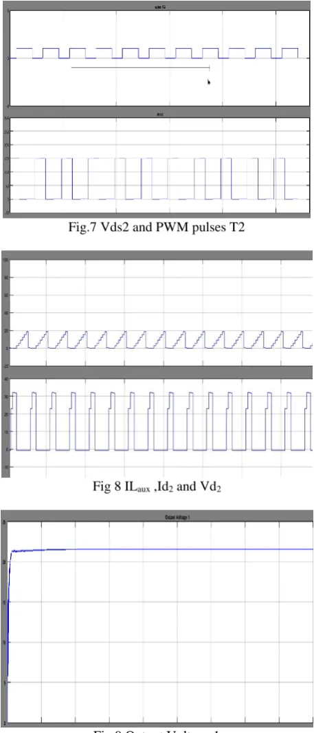
Fig 8 ILaux ,Id2 and Vd2
Fig.9 Output Voltage 1
Fig.10 Output current
© 2017 AJAST All rights reserved. www.ajast.net Fig.11 Current across d1
Fig.12 Voltage across d1
The voltage across d1 is obtained from the voltage measurement across d1.
Fig.13 Output voltage 2
Fig.14 Output current 2
Thus the proposed SIMO converter is studied using MATLAB Simulink model and the results are obtained.
5. DESIGN OF PARAMETERS Vs=12V
Vo=5.2V L1=L2=1mH L01=L02=22µH C1=C2=1µF C0=12000µF D=17.9%
6. HARDWARE CIRCUIT
Fig.15 Hardware implementation
Fig.16 Hardware output
Thus the proposed SIMO converter produces step down voltage with multiple output terminals. The conversion ratio is improved and the output is observed in Multimeter. The switching pulse was generated by using fast PWM technique, because thus the switching frequency of the circuit is 50KHZ.Thus the hardware results are taken for the input voltage of 12V.The voltage of middle voltage switch is steadily clamped. The average efficiency of the proposed converter is 94% and maximum efficiency is 95.9%.
7. CONCLUSION
© 2017 AJAST All rights reserved. www.ajast.net with the property of ZVS to achieve the objective of high
efficiency SIMO step down power conversion;2)the voltage ratio can be increased by using a coupled inductor;3)the stray energy can be recycled by the middle voltage capacitor to ensure the property of voltage clamping;4)an auxiliary inductor is designed for providing the charge power for auxiliary module;5)the copper loss in the magnetic core can be reduced by lower turns in copper film. The experimental results gives an average efficiency of 95.9% and average conversion efficiency as 90%.The auxiliary module implemented in this project can also be extended to other dc loads. It also provides an alternate solution to designers with alternative choices of stepping down the voltages.
REFERENCES
[1] L. Cao, K. H. Loo, and Y. M. Lai, “Systematic derivation of a family of output-impedance shaping methods for power converters—A case study using fuel cell-battery-powered single-phase inverter system,” IEEE Trans. Power Electron., vol. 30, no. 10, pp. 5854–5869, Oct. 2015.
[2] R. G. Wandhare and V. Agarwal, “Novel integration of a PV-wind energy system with enhanced efficiency,” IEEE Trans. Power Electron., vol. 30, no. 7, pp. 3638–3649, Jul. 2015.
[3] K. W. Hu and C. M. Liaw, “Development of a wind interior permanent magnet synchronous generator-based microgrid and its operation control,” IEEE Trans. Power Electron., vol. 30, no. 9, pp. 4973–4985, Sep. 2015.
[4] Mohammed, M.A., Ahmad, M.S. and Mostafa, S.A., 2012, June. Using genetic algorithm in implementing capacitated vehicle routing problem. In Computer & Information Science (ICCIS), 2012 International Conference on (Vol. 1, pp. 257-262). IEEE.
[5] Obaid, O.I., Ahmad, M., Mostafa, S.A. and Mohammed, M.A., 2012. Comparing performance of genetic algorithm with varying crossover in solving examination timetabling problem. J. Emerg. Trends Comput. Inf. Sci, 3(10), pp.1427-1434.
[6] Mohammed, M.A., 2015. Design and Implementing an Efficient Expert Assistance System for Car Evaluation via Fuzzy Logic Controller. International Journal of Computer Science and Software Engineering (IJCSSE), 4(3), pp.60-68.
[7] Mohammed, M.A., Al-Khateeb, B. and Ibrahim, D.A., 2016. Case based Reasoning Shell Framework as Decision Support Tool. Indian Journal of Science and Technology, 9(42).
[8] Mohammed, M.A., Belal, A.K. and Ibrahim, D.A., 2016. Human Interaction with Mobile Devices on Social Networks by Young and Elderly People: Iraq a Case Study. Indian Journal of Science and Technology, 9(42).
[9] Hameed, A.H., Mostafa, S.A. and Mohammed, M.A., 2013. Simulation and evaluation of WIMAX handover over
homogeneous and heterogeneous networks. American Journal of Networks and Communications, 2(3), pp.73-80.
[10] Mostafa, S.A., Ahmad, M.S., Mohammed, M.A. and Obaid, O.I., 2012. Implementing an expert diagnostic assistance system for car failure and malfunction. IJCSI International Journal of Computer Science Issues, 9(2), pp.1694-0814.
[11] Mahdi, O.A., Mohammed, M.A. and Mohamed, A.J., 2012. Implementing a novel approach and convert audio compression to text coding via hybrid technique. International Journal of Computer Science Issues, 9(6), pp.53-59.
[12] Mohammed, M.A., Aljumaili, A.T.Y. and Salah, H.A., 2014. Investigation the role of cloud computing in the business value for optimal criteria. International Journal of Enhanced Research in Science Technology and Engineering, 3(6), pp.111-8.
[13] Mahmood, S.A., Mohammed, M.A. and Farhan, R.N., 2014. Design and Implementation of a Private Cloud Cluster for G-Cloud in IRAQ. International Journal of Enhanced Research in Science Technology and Engineering, 3(5), pp.448-56.
[14] Mohammed, M.A., Investigating Role of Knowledge Auditing in Profile of the Business Unit-Information Technology& Computer Center (ITCC) University of Anbar. International Journal of Enhanced Research in Management & Computer Applications, 4 (3), pp.10-18.
[15] F. Blaabjerg and K. Ma, “Future on power electronics for wind turbine systems,” IEEE J. Emerg. Sel. Topics Power Electron., vol. 1, no. 3, pp. 139–152, Sep. 2013.
[16] K. Xie, Z. Jiang, and W. Li, “Effect of wind speed on wind turbine power converter reliability,” IEEE Trans. Energy Convers., vol. 27, no. 1, pp. 96–104, Mar. 2012.
[17] J. Xu, S. Liao, Y. Sun, X. Y. Ma, W. Gao, X. Li, J. Gu, J. Dong, and M. Zhou,“An isolated industrial power system driven by wind coal power for aluminum productions: A case study of frequency control,” IEEE Trans. Power Syst., vol. 30, no. 1, pp. 471–483, Jan. 2015.
[18] F. Forest, A. T. Meynard, J. J. Huselstein, D. Flumian, C. Rizet, and A. Lacarnoy, “Design and characterization of an eight-phase-137-kW intercell transformer dedicated to multicell dc-dc stages in a modular UPS,” IEEE Trans. Power Electron., vol. 29, no. 1, pp. 45–55, Jan. 2014.