NOTCH FILTER USING SIMULATED
INDUCTOR
D.SUSAN*
Dr.S.JAYALALITHA†
Abstract :
The design of analog filters at low frequencies is not possible because the size of inductors becomes very large. In such cases, the simulated inductors using operational amplifiers are used. This paper deals with the implementation of notch filter using band pass filter which uses simulated inductor where the direct implementation of notch filter using simulated inductor is not possible because of floating inductor. The design of notch filter and the simulation done in PSPICE is presented
Keywords: Notch filter;Generalized Impedance Converter; Simulated Inductor; LCR resonator;
1. Introduction
The use of inductors at low frequency applications is impossible, because, it has the disadvantage that the value of the inductor is high and the size of the inductor is large which makes it bulky [1]. An alternate way of using the inductor at low frequency is to use the simulated Inductor derived from the Generalized impedance converter. The circuit is the Antoniou circuit [2]. This finds many applications such as, realization of analog filter like low pass, high pass etc. [3].
But this has its own limitation in that, the passive component inductor is replaced by the simulated inductor only if, the inductor is a grounded one. In cases like, low pass filter and notch filter where the inductor is floating; some transformation is used to convert the floating inductor to a grounded Frequency dependent negative resistance (FDNR). This is applicable to low pass filter [4] but becomes floating in the case of notch filter. In such case, the concept of obtaining the notch filter from band pass filter using the simulated inductor is presented in this paper.
2. Notch filter from LCR resonator 2.1. Basic LCR resonator
2.2.Notch filter from band pass filter
There are several ways to make a notch filter [5] .One simple technique is to subtract the band pass filter from its input [6]. This principle is illustrated in the block diagram as shown in the figure 4. The band pass filter has an inverted output as the gain or transfer function is negative. While implementing, a summer is used instead of a subtractor. Also, the band pass filter has a gain of Ao so that the output at the centre frequency will
be –AoVi. To completely subtract this output, the input of the summer must be precisisely AoVi. Thus a gain of
Ao must be added between the input signal and the summer as shown in the block diagram. Figure 1. Basic LCR Resonator circuit
Figure 2. Basic notch filter circuit from LCR resonator
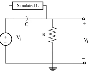
Figure 3. Notch filter from LCR resonator circuit showing the floating Inductor
R C
Vr
x y z
L
Vi
L
R C
SimulatedL
Vi R V
0
+
_ +
_
The output of the circuit in the s domain is given by the equation
(
)
2(
2)
)
(
o o i o o i o os
s
s
sV
A
s
V
A
s
V
1
2 2)
(
)
(
o o o o i os
s
s
A
s
V
s
V
2 0 2 2 2)
(
o o os
s
s
A
which is the response of the notch filter.o
is the notch frequency and
is the damping factor which decides the quality factor2.3.Design of Notch filter
The notch filter is designed for 50Hz which is highly useful in the rejecting single frequency, such as the power line frequency hum.
Hz
f
o
50
so thatL
10
.
142
H
C
1
F
To simulate L=10.142 H, the value of R=3.184KΩ and C= 1µF for the circuit given in the figure 5 for simulating L.
2.4.Implementation of Notch filter
2
2
o
o
s
s
o
o
A
o
A
V
o
(s)
Vo(s)
Bandpass filter
Block diagram of notch from band pass filter
+
_
_
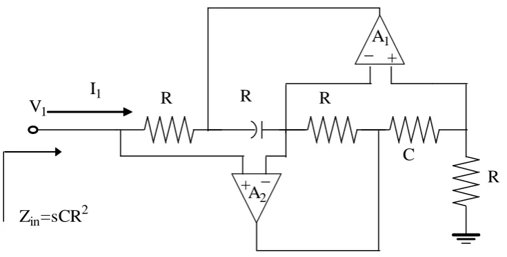
+
V
1I
1R
R
R
C
R
A
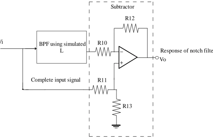
1The basic band pass filter using simulated L is shown in the Figure 6. The output of this response and the complete input signal with proper gain is given to the subtractor to get the response of the notch filter and the block diagram is given in the Figure 7. The various resistances in the subtractor namely R10, R11, R12, R13 is
properly choosen to get the desired gain
Vi R
C
V0 +
_ +
_
Si
m
u
la
te
d
L
Figure 5. Band pass filter with grounded Simulated L
BPF using simulated L
Vi R10
R11
R13 R12
Vo
Complete input signal
Response of notch filter Subtractor
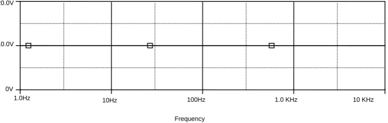
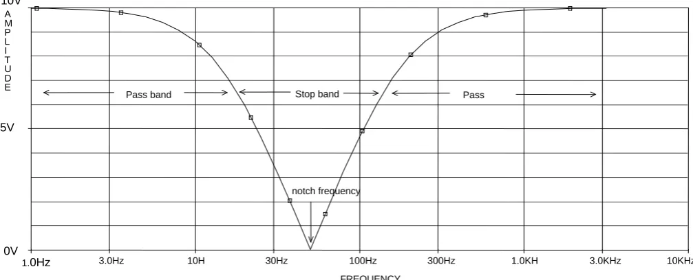
The frequency response of the band pass filter is shown in the Figure 8 and complete input signal with proper gain is shown in the Figure 9. The frequency response of the notch filter is shown in the Figure 10.
Figure 7. Response of band pass filter given to one terminal of subtractor
Figure 8. Complete input signal given to one terminal of subtractor
Frequency
10Hz 100Hz 1.0 KHz 10 KHz 0V
10.0V 20.0V
1.0Hz
FREQUENCY
3.0Hz 10Hz 30Hz 100Hz 300H 1.0KHz 3.0KHz 10KHz 30KHz 100KHz 0V
5V 10V A M P L I T U D E
fo
Stop Stop band Pass band
3. Conclusion
The response of notch filter using simulated inductor is obtained using PSPICE and presented. The filter is designed for a frequency of 50Hertz, which is the notch frequency in many systems to eliminate the hum at supply frequency. The need for bulky, heavy and expensive inductors can be dispensed with for realizing very low frequencies. Thus by using the grounded inductor, it is possible to obtain a notch filter from the band pass filter which is not realized so far using the method mentioned in this paper.
References
[1] Umesh Kumar and Sushil Kumar Shukla, “Analytical study of inductor simulation circuit”active and passive Elec.comp 1989, vol. 13, pp 211-227
[2] Sedra and Smith, Microelectronic Circuits, Fourth Edition 2002, Oxford University Press
[3] D.Susan, S.Jayalalitha, “ Analog filters using Simulated Inductor”, 2nd International Conference on Mechanical and Electrical
Technology ( ICMET), September 2010, pp 659-662, Singapore.
[4] D.Susan, S.Jayalalitha, “Synthesis of low pass filter using FDNR”, International Journal of Advanced Engineering and Research, 2010.
[5] George S Moschytz, “Inductorless filters:a survey II.Linear active and digital filters”,IEEE spectrum,September 1970,pp 63-75 [6] Sergio Franco, “Design with operational Amplifiers and Analog Integrated circuits”, Second Edition, 2007, McGraw Hill International
Editions
Figure 9. Response of Notch filte FREQUENCY
3.0Hz 10H 30Hz 100Hz 300Hz 1.0KH 3.0KHz 10KHz
0V 5V 10V
A M P L I T U D E
notch frequency
Stop band Pass
Pass band