www.iosrjen.org
Comparative simulation study between n- type and p- type Silicon
Solar Cells and the variation of efficiency of n- type Solar Cell by
the application of passivation layer with different thickness using
AFORS HET and PC1D
.U.Gangopadhyay, S. Roy, S.Garain, S. Jana, S.Das
Meghnad Saha Institute of Technology (TIG), Nazirabad, Kolkata-700107.
ABSTRACT : - In this paper, comparative study of p type and n type solar cells are described using two popular solar cell analyzing software AFORS HET and PC1D. We use SiNx layer as Antireflection Coating and
a passivated layer Al2O3 .The variation of reflection, absorption, I-V characteristics, and internal and external
quantum efficiency have been done by changing the thickness of passivated layer and ARC layer, and front and back surface recombination velocities. The same analysis is taken by imposing surface charge at front of n-type solar Cell and we get 20.13%-20.15% conversion efficiency.
Keywords:- ARC coating, Surface recombination velocity, Passivation layer, Surface charge, AFORS HET, PC1D
I. INTRODUCTION
Solar energy is an abundant source of green energy .It plays a crucial role due to increasing price of
fossil fuel and acute shortage of them which also leads to global warming. At present more than 85% of the industrial solar cells are fabricated based on p type silicon material. The n-type solar cell is one of the interesting technological solution basically due to its lower recombination velocity, tolerance of higher temperature, higher carrier lifetime [1]. It offers high stabilized cell efficiencies because they do not suffer from light induced degradation(LID) caused by the simultaneous presence of boron and oxygen in the wafers[2], a phenomenon that in standard p-type silicon solar cells leads to a reduction of the module power output by usually two to three percent within the first weeks of installation. Second, n-type Si wafers are less sensitive to impurities that are usually present in silicon feedstock; consequently, fewer efforts have to be made to obtain n-type Si wafers with a high electronic quality.
On the other hand, one of the important reasons for decreasing efficiency for solar cell is the reflection
of light from the air/silicon interface. This reflection reduces the external quantum efficiency. So an adequate
layer of antireflection coating (ARC) can be used to match the optical impedance and reduce the reflection. SiNx
is most popular and commercially available ARC [3]. But SiNx layer induces a positive surface charge density
of the order of 1012 cm-2[2, 4], so it has a detrimental effect on the efficiency of p+ / n or p+/n/n+ c-Si solar cell.
To achieve a solar cell with higher efficiency, a highly effective surface passivation of the cell both at front and
rear, should be required. Lower recombination velocity is achieved by using this passivation layer. Al2O3acts as
good passivation layer [5]. So Al2O3 is sandwiched between SiNx and p+ emitter of n type Solar cell. Weighted
reflectance for Al2O3/SiNx ARC stack is 10.50% [6] and it reduces the front surface recombination velocity
upto10cm/s[7]. Al2O3 is a wide band gap dielectric (8.8 eV) with dielectric constant around 9 [8].
The aim of this study is to analysis the performance of the n-type solar cell and represents a comparison
with p- type Solar cell using PC1D and AFORS HET. We also study the effect of positive and negative surface charges on the front surface of the n-type Solar Cell. To achieve maximum efficiency of n-type solar cell, we optimized the passivated layer thickness and the recombination velocity. This simulation is done by PC1D due to some difficulties facing during simulation with AFORS HET to increase the performance of solar cell.
II. SIMULATIONANDRESULTS
The structure for the modeling of crystalline silicon solar cells used in this paper as shown in Fig.1.
The background doping density of n-type base is 1016cm-3, and its thickness is 200μm. The p+ emitter has a peak
density of 1019cm-3at the front surface, with the sheet resistance of ~100Ω/cm2 and the emitter junction depth of
(a) (b)
Fig 1: schematic diagram of simulated c-Si solar cell structure (a) n+pp+ and (b) p+nn+
The rear diffusion has a peak intensity of 1019cm-3with junction depth and sheet resistance. The
electron and hole lifetime parameters were set at 100μs, for both n-type and p-type, the corresponding diffusion
length of 400 µm and 139 µm respectively, with the background doping density of 1×1016cm-3at the temperature
of 300K. The front and back surface recombination velocities (FSRV) are about 1×106cm/s. The standard
AM1.5G was chosen as the illumination source, corresponding to an intensity of 0.1W/cm2at 25°C. In addition,
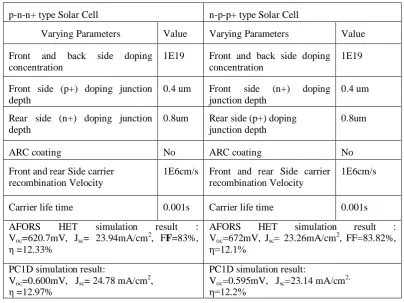
the texture depths of the front and rear surface were both 0.4μm, some important solar parameters of crystalline silicon solar cells are used in the simulations were shown in Table-1, and all of the other parameters were the default values in PC1D. Here both p- type and n-type cells are simulated and they both show more or less 12% efficiency.
Table 1: Variation of different parameters of N type Solar Cell
II.I AFORS HET SIMULATION GRAPHS FOR N TYPE SOLAR CELL
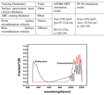
The reflection and transmission curve of the Solar cell at the particular condition using AFORS HET is
shown in table 1. It has been observed that the Solar cell shows 40% reflectance, so the residual of the light should be absorbed into the cell.
p-n-n+ type Solar Cell n-p-p+ type Solar Cell
Varying Parameters Value Varying Parameters Value
Front and back side doping concentration
1E19 Front and back side doping
concentration
1E19
Front side (p+) doping junction depth
0.4 um Front side (n+) doping
junction depth
0.4 um
Rear side (n+) doping junction depth
0.8um Rear side (p+) doping
junction depth
0.8um
ARC coating No ARC coating No
Front and rear Side carrier recombination Velocity
1E6cm/s Front and rear Side carrier recombination Velocity
1E6cm/s
Carrier life time 0.001s Carrier life time 0.001s
AFORS HET simulation result :
Voc=620.7mV, Jsc= 23.94mA/cm2, FF=83%,
η =12.33%
AFORS HET simulation result :
Voc=672mV, Jsc= 23.26mA/cm2, FF=83.82%,
η=12.1%
PC1D simulation result:
Voc=0.600mV, Jsc= 24.78 mA/cm2,
η =12.97%
PC1D simulation result:
Voc=0.595mV, Jsc=23.14 mA/cm2,
200 400 600 800 1000 1200 -0.1
0.0 0.1 0.2 0.3 0.4 0.5 0.6 0.7 0.8 0.9 1.0
Transmission Reflection
Fr
ac
tion*100
Wavelength(nm)
Fig.2: Reflectance and Transmittance curve for different wavelengths
Neglecting the scattering and dispersion phenomenon the summation of reflection, absorption, and
transmission will be 100%. In fig. 2 due to zero transmissions the residual light should be absorbed into the bulk material of the cell. Fig 3 shows the absorption with wavelength.
200 400 600 800 1000 1200 -0.1
0.0 0.1 0.2 0.3 0.4 0.5 0.6 0.7
Layer 3
Layer 2 Layer 1
Abso
rptio
n*100
Wavelength(nm)
Fig.3: Absorbance curve for different wavelengths
The Fig. 4 indicates the simulated I-V curve of n-type solar cell. The open circuit voltage (Voc) is the
potential difference that is developed between the two terminals of the cell when external load resistance is large and the short circuit current (Isc) is the current when load resistance is zero. The Isc and Voc are the key parameters for efficiency of the solar cell.
-0.7 -0.6 -0.5 -0.4 -0.3 -0.2 -0.1 0.00.000 0.005 0.010 0.015 0.020 0.025
Current d
ensit
y(A
/cm
2
)
Voltage(V)
Fig.4.Current Vs Voltage curve of the Solar Cell
For increasing efficiency, the antireflection coating SiNx is usually used on both p- type and n-type
solar cell. Because of the high positive charge density of SiNx film serves a poor performance for n-type solar
cell than p-type [6]. The comparative result is shown in table 2.
Table2: Variation of efficiency in p- type and n- type Solar cell after giving SiNx ARC
Description of ARC Conversion Efficiency
PECVD(SiNx) ARC coating
thickness=75nm, refractive index=2.1
N type P type
Surface recombination velocity plays an important role on the variation of short circuit current and open circuit voltage. Higher recombination rates at the top surface give a detrimental impact on short circuit current. Top layer surface recombination can be reduced by decreasing the dangling bonds of Silicon by using a passivation layer. It has already been reported that due to the presence of oxide layer Al2O3 serves as a good
passivation layer for n type solar cell [5-7]. So in this paper Al2O3 is used to neutralize these dangling bonds
which lead to decrease the surface recombination velocity (SRV) and increases the minority carrier lifetime.
Table 4 shows the simulation result after giving Al2O3 on the surface of Si and above which we apply SiNx
Anti-Reflection coating [6]. The following result gives higher efficiency than the efficiency obtained in table 1 and
2.Al2O3/SiNx stack layer reduces the FSRV up to 10cm/s[6].But before that operation SRV we adjust SiNx and
Al2O3 thickness for maximizing the efficiency[6].
The schematic structure of the p+nn+ crystalline silicon (c-Si) solar cell is used during simulation
(AFORS HET) with SiNx ARC and Al2O3 passivated layer as shown in Fig.5
Fig.5 Schematic diagram for p+nn+ with SiNx ARC and Al2O3 passivation layer
Table 3: Variation of efficiency with the variation of thickness with Al2O3 and SiNx AR coating
Table 4: Variation of efficiency with the variation surface recombination velocity with Al2O3and SiNx AR
Coating
The final simulation analysis after development of Al2O3/SiNx film above the emitter layer of n-type
cell shows efficiency raises up to 7 % than the without Al2O3/SiNx film on n type solar cell. The result is given
below.
Al2O3 thickness (nm) SiNx thickness (nm) Efficiency ((%)
60 70 14.06
50 70 14.9
40 70 15.81
30 70 16.98
20 70 17.85
10 70 18.41
10 65 18.59
10 50 18.38
10 40 17.67
Front Surface Recombination
Velocity (cm/s2)
Rear surface Recombination
Velocity (cm/s2)
Efficiency (%)
1000 10000 19.94
100 10000 19.97
10 10000 20.12
10 1000 20.28
10 100 20.3
10 10 20.15
8 100 20.15
Table 5: Variation of different parameters of N type Solar Cell
200 400 600 800 1000 1200
-0.1 0.0 0.1 0.2 0.3 0.4 0.5 0.6 0.7 0.8 0.9 1.0
Transmission Reflection
Fractio
n*100
wavelength(nm)
Fig.6 Reflectance and Transmittance curve for different
The reduction in reflection indicates the increase of absorption in bulk layer. We observed that the
absorption is increases to 20% than the previous analysis as shown in Fig.7. The I-V characteristics graph as shown in Fig.8 provides a higher short circuit current density than the initial one. This implies due to the reduction of reflection and increasing the absorption the rate of generation of carriers has been raised, which increases the efficiency up to 20.13%. The simulation analysis shows standard reflection graph after giving
Al2O3/SiNx stack layer, which is shown in Fig 6.
200 400 600 800 1000 1200
-0.1 0.0 0.1 0.2 0.3 0.4 0.5 0.6 0.7 0.8 0.9 1.0
layer3
layer2
layer1
A
bso
rptio
n*100
Wavelength(nm)
Fig.7 Absorbance curve for different wavelength
Varying Parameters Value AFORS HET
simulation result
PC1D simulation result
Surface passivation layer (Al2O3) thickness
10nm
ARC coating thickness 60nm
Voc=750.3mV
Jsc=37.12A/cm
2
FF=72.33%,
η =20.15%
Voc= 676.2mV
,Jsc= 35.3A/cm2,
η =20.13%
Front surface
recombination velocity
10cm/s
Rear Surface
recombination velocity
-0.8 -0.7 -0.6 -0.5 -0.4 -0.3 -0.2 -0.1 0.00.000 0.005 0.010 0.015 0.020 0.025 0.030 0.035 0.040
Current d
ensit
y(A
/cm
2
)
Voltage(V)
Fig.8 Current Vs Voltage curve of the Solar Cell
II.II QUANTUM EFFICIENCY VARIATION OF N TYPE SOLAR CELL WITH FSRV
The "quantum efficiency" (Q.E.) is the ratio of the number of carriers collected by the solar cell to the
number of photons of a given energy incident on the solar cell. The quantum efficiency may be given either as a function of wavelength or as energy. If all photons of a certain wavelength are absorbed and the resulting
minority carriers are collected, then the quantum efficiency at that particular wavelength is unity. It is
measured in electrons per photon or amps per watt. There are two types of quantum efficiency is generally considered. External quantum efficiency (EQE) which is the ratio of the number of charge carriers collected by the solar cell to the number of photons of a given energy incident on the solar cell from outside and the another one is internal quantum efficiency (IQE). It indicates the ratio of the number of charge carriers collected by the solar cell to the number of photons of a given energy that shine on the solar cell from outside and are absorbed by the cell. So the surface recombination velocity makes a deep impact on the variations of IQE and EQE. Higher surface recombination velocity implies that the rate of generation of charge carriers in the Solar cell reduces. So the IQE and EQE both must also be decreased with the increasing of surface recombination velocity. The simulation of the variation between front surface recombination velocity and IQE or EQE has been done by using both type of simulator such as PC1D and AFORS HET. The results are shown in the Fig. 9, 10, 11 and 12 respectively.
400 600 800 1000 1200
0 20 40 60 80 100
FSRV=103
cm/s FSRV=104
cm/s FSRV=105
cm/s FSRV=106
cm/s FSRV=107
cm/s FSRV=10 cm/s
EQE
Wavelength(nm)
Fig9. Variation of EQE with different FSRV by using PC1D
300 400 500 600 700 800 900 1000 1100 1200
0 20 40 60 80 100
FSRV=107 cm/s FSRV=106cm/s FSRV=105
cm/s FSRV=104cm/s FSRV=103
cm/s FSRV=10cm/s
EQE
Wavelength(nm)
Fig.9 and Fig.10 shows the variation of EQE with different FSRV. Both of the graphs indicate that the EQE reduces with the increase of FSRV due to the loss of carriers. In a similar way IQE also decreases with the increasing of FSRV. These results are shown in Fig. 11 and Fig.12 respectively.
300 400 500 600 700 800 900 1000 1100 1200 1300 0
10 20 30 40 50 60 70 80 90 100
IQ
E
FSRV=10cm/s FSRV=103
cm/s FSRV=104
cm/s FSRV=105
cm/s FSRV=106
cm/s FSRV=107
cm/s
Wavelength(nm)
Fig11. Variation of IQE with different FSRV by using PC1D
300 400 500 600 700 800 900 1000 1100
20 40 60 80 100
FSRV=107 cm/s FSRV=106
cm/s FSRV=105cm/s FSRV=104cm/s FSRV=103cm/s FSRV=102
cm/s
IQ
E
Wavelength(nm)
Fig12. Variation of IQE with different FSRV by using AFORS HET
II.III SURFACE CHARGE DENSITY ROLE ON SOLAR CELL EFFICIENCY
Now a different approach is performed by applying surface charge density at the front and rear surface
of n-type Solar Cell [6]. Application of Surface charge density on the buffer layer Al2O3 enhances or reduces the
recombination at the surface of the cell. This fact entirely depends upon the type of the polarity of the surface charge, doping of semiconductor layer and the type of buffer material. So positive and negative charge density has been imposed alternatively on the front surface of the cell and investigates the result. The effect of surface charge density is shown using PC1D simulation. For the simulations of Solar cell here FSRV 5000 cm/s, RSRV 100 cm/s is taken It has been observed from PC1D simulation results as shown in Fig.13 and table-7 that efficiency of the p+nn+ is increases with the presence –ve surface charge density on the front surface and
maximum at -6.88×1012 cm2. This amount of –ve charge can give maximum efficiency 19.87% of p+nn+
crystalline silicon solar cell(c-Si). On the other hand the efficiency of the c-Si solar cell is decreases with increase of +ve surface charge density as indicated in the Fig.13 and table-7.
-6.0x10¹²-3.0x10¹² 0.0 3.0x10¹² 6.0x10¹² 9.0x10¹²
18.0 18.4 18.8 19.2 19.6 20.0
Ef
ficiency
%
Front surface charge density(cm-2)
Table7: Change of Efficiency with the variation of Surface charge at SRV FSRV=5000cm/s, RSRV=100cm/s
III. CONCLUSION
We have reported that the fabrication process of n-type solar cells based on surface passivation layer
leads to a record efficiency of 20.1% for large area crystalline silicon solar cell, while the same process on p-type solar cell resulted in 18.2% efficiency. By improving the front surface passivation somewhat higher efficiencies can still be obtained on n-type wafers by this process. High efficiencies may also be received on n-type solar cell
if the –ve surface charge is imposed on the c-Si solar cell front surface by thin layer of Al2O3 passivated layer.
With proper optimization of front surface charges more efficiency will be envisioned.
Acknowledgements
The authors deeply acknowledge Meghnad Saha Institute of Technology, TIG provides the
infrastructural support for carrying out research activity in this area. The authors also gratefully to acknowledge the DST, Govt. of India for financial support for carrying out solar cell related research activity.
REFERENCES
[1] A.Cuevas, M.J.Kerr, C.Samundsett, F.Ferraza, G.Cotelti, “Millisecond minority carrier lifetime in n-type multicrystalline silicon”, Appl. Phys. Lett.,81(2002) 4952-4954.
[2] Arnab Das,Kyungsun Ryu,Ajeet Rohatgi,”20% Efficient Screen-Printed n-type Solar Cells Using a Spin On source and Thermal
Oxide/Silicon Nitride Passivation”, IEEE journal of Photovoltaic,Vol..1,No.-2,December(2011),Page-146-148. [3] K Chandra Sahoo, Yiming Li, Edward Yi Chang, Men-Ku Lin, Jin-Hua Hung, “ Reflectance of Sub-Wavelength Structure on Silicon
Nitride For Solar Cell Application”, Proceeding of IEEE Specialist Conferrence(2009),Page-123.
[4] I.Martin,R.Lovblom,R.Alcubilla,”High Efficiency Solar Cells Based on Inversion layer Emitters.”,24th European Photovoltaic Solar Energy Conference, 21-25th September(2009),Hamberg,Germany,Page-1988.
[5] K.J.Weber,H.Jin,C.Zhang,N.Nursan,W.E Jellett,K.R.McIntosh,”Surface Passivation using dielectric films: How much charge is enough?”,24th European Photovoltaic Solar Energy Conference, 21-25th September(2009),Hamberg,Germany,Page- 534.
[6] Wu Dawei., JiaRui, Ding Wuchang,Chen Chen, Wu Deq,Chen Wei, Li Haofeng, YueHuihui, and Liu Xinyu. “Optimization of Al2O3/SiNx stacked antireflection structures for N-type surface passivated crystalline silicon solar cellsJournal of Semiconductors, ” Vol. 32, No. 9 ,September(2011), Page-094008-1to-094008-2.
[7] J.Benick,B.Hoex,G.Dingemans,W.M.MKessels,A.Richter,M.Hermle,S.W.Glunz, “High Efficiency N-type Silicon Solar Cells With Front Side Boron Emitter”, 24th European Photovoltaic Solar Energy Conference, Hamburg ,Germany, 21-25th September(2009),Page-863.
[8] Gang He,Xiaoliang Wang,Masaharu Oshima,Yukihiro Shimogaki,” Metalorganic Chemical Vapour Deposition of Al2O3 thin film from Dimethyl aluminiumhydride and O2”.Japanese Journal of Applied Physics,Vol-49(2010),Page-031502-4.
Surface Charge (cm-2)
Efficiency (%)
Short circuit current
density(mA/cm2)
Open circuit voltage(mV)
-8E12 19.77 36.17 -655.1
-7E12 19.91 36.24 -657.9
-6E12 19.9 36.24 -657.9
-5E12 19.9 36.24 -657.7
-4E12 19.89 36.24 -657.5
-3E12 19.87 36.23 -657.2
-2E12 19.86 36.22 -656.8
-1E12 19.84 36.21 -656.4
0 19.78 36.18 -655.3
1E12 19.7 36.14 -653.6
2E12 19.62 36.08 -651.8
3E12 19.47 35.99 -648.8
4E12 19.25 35.84 -644.7
5E12 18.95 35.61 -639.4
6E12 18.56 35.27 -633
7E12 18.39 35.1 -630.5
![Table 4 shows the simulation result after giving Al2O3 on the surface of Si and above which we apply SiNx Anti-Reflection coating [6]](https://thumb-us.123doks.com/thumbv2/123dok_us/8358146.1669912/4.595.117.479.569.707/table-shows-simulation-result-giving-surface-reflection-coating.webp)