International Journal of Electronics Communication and Computer Engineering Volume 3, Issue 4, ISSN (Online): 2249–071X, ISSN (Print): 2278–4209
Efficient Implementation of Maximum Power Point
Tracking Using Perturb and Observe Method
Sonali Surawdhaniwar
Raipur Institute of Technology,Raipur (Chhattisgarh) INDIA [email protected]
Mr. Ritesh Diwan
Raipur Institute of Technology,Raipur (Chhattisgarh) INDIA
Abstract - Solar energy and photovoltaic system are used to power the embedded system and other mobile devices. Since, the output characteristics of a photovoltaic array vary nonlinearly when temperature or irradiance conditions change, the maximum power cannot be achieved by directly connecting the PV models. Tracking of the Maximum Power Point (MPP) must be used to effectively get the maximum output power. According to Maximum Power Transfer theorem, the power output of a circuit is maximum, when the Thevenin impedance of the circuit or source impedance matches with the load impedance. Hence, our problem of tracking the maximum power point reduces to an impedance matching problem and also improves the efficiency of the solar panel. The improved MPPT technique, which is constructed with close loop control system with DC to DC converter and also follow the basic requirements of MPPT ie., temperature and radiation.
Keywords - DC/DC Converter, Photovoltaic System, maximum Power Point Tracking.
I. I
NTRODUCTIONRenewable energy is the energy which comes from natural resources such as sunlight, wind, rain, tides and geothermal heat. These resources are renewable and can be naturally replenished. Therefore, for all practical purposes, these resources can be considered to be inexhaustible, unlike dwindling conventional fossil fuels. The renewable energy resources supplement the main electrical power and eliminate batteries which are provide power to small (Micro or even nano) autonomous devices that are operational all the time. The work on the various methods of maximum power point tracking has been studied. Studies show that maximum power point tracking is necessary to increase the efficiency of the solar panel. There are different techniques for MPPT such as perturb and observe, incremental conductance, fractional short circuit current, fractional open circuit voltage, fuzzy control, neural network control [1] etc.
Renewable energy generation [2] has experienced consistent growth in the last two decades, motivated by the concerns of climate change and high oil prices, and supported by renewable energy legislation and incentives, with a close to $150 billion investment in 2007. Solar photovoltaic’s is one of the fastest growing energy technologies, with an average annual growth of about 40% in the past decade. [2 of newest]. The 2.6GW installed
compared to the previous year and has lead to a total capacity of 7.8GW photovoltaic power worldwide (Fig. 1(a)). Similarly high grow rate has been registered in the past few decades for the wind power industry as well, with an approximately 30% increase in 2007.
Despite the technological advances and governmental incentives, the cost of energy produced by grid connected PV systems is still relatively high and cannot compete yet with traditional wholesale electricity prices. This motivates the research for creating not only improved solar panels but also more efficient power converters which can extract close to 100% of the available power from the photovoltaic array [3].
Fig.1. Cumulative installed (a) and percentage of grid connected and off-grid (b) PV power.
Recently, the installation of PV generation systems is rapidly growing due to concerns related to environment, global warming, energy security, technology improvements and decreasing costs. PV generation system is considered as a clean and environmentally-friendly source of energy. The main applications of PV systems are in either standalone or grid connected configurations. Standalone PV generation systems are attractive as indispensable electricity source for remote areas . However, PV generation systems have two major problems which are related to low conversion efficiency of about 9 to 12 % especially in low irradiation conditions and the amount of electric power generated by PV arrays varies continuously with weather conditions. Therefore, many research works are done to increase the efficiency of the energy produced from the PV arrays [3].
International Journal of Electronics Communication and Computer Engineering Volume 3, Issue 4, ISSN (Online): 2249–071X, ISSN (Print): 2278–4209
power point tracking (MPPT) techniques are needed to maintain the PV array’s operating point at its MPP. Many MPPT techniques have been proposed in the literature in which the techniques vary in many aspects, including simplicity, convergence speed, hardware implementation and range of effectiveness. However, the most widely used MPPT technique is the perturbation and observation (P&O) method [5].
The P&O MPPT algorithm is mostly used, due to its ease of implementation. It is based on the following criterion: if the operating voltage of the PV array is perturbed in a given direction and if the power drawn from the PV array increases, this means that the operating point has moved toward the MPP and, therefore, the operating voltage must be further perturbed in the same direction. Otherwise, if the power drawn from the PV array decreases, the operating point has moved away from the MPP and, therefore, the direction of the operating voltage perturbation must be reversed. This paper presents a simple MPPT algorithm which can be easily implemented and adopted for low cost PV applications.
1.1 Maximum Power Point Tracking
A typical solar panel converts only 30 to 40 percent of the incident solar irradiation into electrical energy. Maximum power point tracking technique is used to improve the efficiency of the solar panel. According to Maximum Power Transfer theorem, the power output of a circuit is maximum when the Thevenin impedance of the circuit (source impedance) matches with the load impedance. Hence our problem of tracking the maximum power point reduces to an impedance matching problem. A simple Maximum Power Point Tracking System is shown below. A simple MPPT-PV Standalone Power System is presented which consists of an array of photovoltaic module (power source), a resistive load and a step-up switching mode DC-DC converter to act as power interface between the PV array and load.
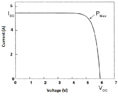
Fig.2. Block Diagram of Proposed MPPT System One significant problem in PV power system is the probable match between the operating characteristics of the load and the PV array. Maximum Power Point tracking is specifically designed to remove the mismatch. Shown in Figure 3 is a standard I-V curve for a PV panel, with X-axis representing voltage and the Y-X-axis representing current.
Fig.3. I-V characteristics of a solar panel
When a PV array is connected to a load directly the system’s operating point will be at the intersection of I-V curve of PV array and load. Under most conditions, this operating point may not be at the PV array’s MPP (represented as point A), which is clearly shown in figure 4.
Fig.4. Current-Voltage Curve of PV cell Fundamental Parameters of Photovoltaic Cell are ISC (Short Circuit Current) : It is the PV output current under Short-Circuit condition.
Voc (Open Circuit Voltage) : It is the voltage value of PV cell when its output current is zero.
MPP (Maximum Power Point) : It represents the maximum power level of a PV’s output under specific condition. The point A in Figure 4 shows this point.
International Journal of Electronics Communication and Computer Engineering Volume 3, Issue 4, ISSN (Online): 2249–071X, ISSN (Print): 2278–4209
Fig.5. (a) P-V characteristics of Photovoltaic Array for Various Values of Temperature at Constant Irradiation (b)
P-V characteristics of Photovoltaic Array for Various Values of Insolation at Constant Temperature. Figure 5(a) shows the MPP shifts with the cell temperature change, and Figure 5(b) represents that it moves with insolation change. In reality, the change of array temperature that it moves the MPP in a large range along X-axis and changing irradiation varies array power output dramatically with little maximum operating voltage (VMPOP) shift.
In reality it is impossible to consider solar insolation and photovoltaic array temperature separately because they are highly coupled under ordinary operating conditions. This statement implies that an increase in the insolation on PV module will be accompanied by an increase in the module temperature as well. Therefore, it seems the tracking control of maximum power point is even complicated. To overcome this problem, a power interface (such as DC/DC converter or DC/AC inverter) controlled by maximum power point tracking (MPPT) controller can be used to maintain the PV array’s operating point at the maximum power operating point (MPOP).
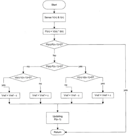
1.2 Maximum Power Point Tracking Algorithm There are several algorithms for calculating the maximum power point. In this paper we represent simple algorithm for the Perturb and Observe (P&O) Method. The basic algorithm for P&O Method is shown below Figure 6[6,7]. The P&O tracking method is very easy for digital control implementation. But the array voltage is perturbed every control cycle based on this method. Therefore, the P&O algorithm will oscillate around the optimal voltage when the maximum power operating point is reached. This results in a waste in PV power delivery, which depends on the step width ‘c’, a constant perturbation. If the step width is selected large, this MPPT algorithm will respond quickly to the sudden changes in operating conditions with the trade-off of poor steady state performances. If the step width is very small, the losses under stable or slowly changing conditions will be reduced, but the system cannot respond to rapid changes in insolation or temperature. The value of the suitable step size width needed be tuned experimentally in the specific systems and environment.
Fig.6. Flow Chart of the P&O MPPT Algorithm In [8,9], the drawback of P&O method is discussed and analyzed further that the dynamic response is slow in cases of rapidly varying atmospheric conditions. When a sudden increase in insolation, The P&O algorithm reacts as if the increase occurred as a result of previous perturbation of the array operating voltage. The next perturbation, therefore, will be in the same directions as the previous one. Assuming that the system has been oscillating around the MPP, it can be seen in Figure 7 that a continuous perturbation in one direction will lead to an operating point far away from the actual MPP. This process continues until the increase in insolation slows down or ends. The reason for this problem is that the output power increase is dominated by solar insolation over control signal, and at this moment the control voltage goes to wrong direction.
Fig.7. Deviation From the MPP Caused by P&O Algorithm under Rapid Increasing Irradiation Levels. 1.3 The Improved P&O Algorithm
International Journal of Electronics Communication and Computer Engineering Volume 3, Issue 4, ISSN (Online): 2249–071X, ISSN (Print): 2278–4209
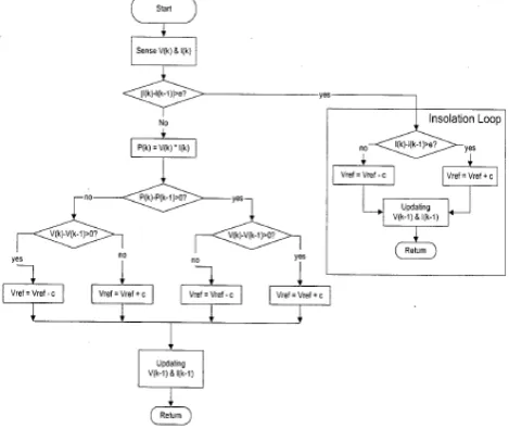
Figure 8 shows the flowchart of control algorithm. An additional insolation control loop is proposed in this modified version. If there is a large and sudden change in the array output current, it can be supposed that this is due to a sudden change in insolation, which is caused by fast moving clouds. A current change threshold ‘e’ needs to be defined as a system parameter. The direction of the array output current is used to directly control the perturbation direction of the array reference voltage. With this additional control loop, fast tracking was achieved. But the difficulties in choosing the voltage incremental step ’c’ and current threshold ‘e’ remain unsolved.
Fig.8. Flow Chart of the Improved P&O MPPT
Algorithm
II. M
ETHODOLOGYFig.9 Proposed Block Diagram for P&O Method for MPPT
In this paper we present a very simple method for tracking the maximum power point using Perturb and Observe (P&O) Method. The circuit is simulated in Matlab, below we explain the working of basic components used.
2.1 Solar Input (PV Module) : There are some materials, which are photo sensitive and they find a place in photo voltaic conversion. A junction of materials, which have
different electrical properties semiconductors are used in solar cells, provides the electrical field in most solar cells. Semiconductors are a class of materials with conductivity somewhere between metals and insulators. Solar cells are manufactured from monocrystalline materials. Low cost cells are round because they are made from sheets, which are cut from monocrystalline rods as they are pulled from the melt [3]. Joining p and n type material in to a single crystal makes the cross section of a silicon solar cell. Single crystal silicon of ultra high purity is doped through its bulk with phosphorus to produce n type silicon. The surface of the wafer is subsequently doped with boron to produce p type silicon. This is p-n junction solar cell.
The photovoltaic effect is the generation of an electrical potential when absorbed radiation, ionizes atoms in the vicinity of an electrical potential barrier (p-n junction). If radiation level is sufficiently separated, electron –hole pairs (EHP) are created in turn creating an EMF capable of causing a current flow through an electrical load. The incident photon energy must equal or exceed the valence to conduction band gap in order to produce electron–hole pairs. These carriers in turn migrate to the created by photon –electron energy transfer migrates towards the p-layer, the current flow is induced.
FUNCTIONING OF SOLAR PANEL: The solar cells is divided in to p-type and n-type layers, the top layer which is exposed to sunlight acts as a p-type layer and the bottom layer which is not exposed to sunlight acts as a n-type layer.
The two layers are fused together the fused area is known as the junction. Fusing of two layers is known as the semi conductors. The function of the solar cell is as similar to a semi conductor. The positive terminal, which is exposed to sunlight, is P Type and the negative terminal is n Type. This is known as forward bias. Holes in P layer are repelled by the positive voltage and the electrons in the n layer are repelled by the negative voltage applied. Therefore the holes and electrons moves towards the junction. Near the junction electron-hole combination takes place.
The electron is liberated from the p-region and enters the terminal. The process continues. Thus a large number of electrons will be flowing from negative to positive terminal. Thus a current is flowing through the junction. The maximum efficiency of 14% is obtained at a temperature of 28 degrees.
2.2 Boost Converter: In [11] boost converter is a power converter with an output DC voltage greater than its input DC voltage. It is a class of switching-mode power supply containing at least two semiconductor switches (a diode and a transistor) and at least one energy storage element. Filters made of capacitors in combination with inductors are normally added to the output of the converter to reduce output voltage ripple. By implementing the pulse width modulation technology (PWM) techniques on the boost converter, a stable output voltage from a non stable input voltage can be obtained by changing the duty cycle of the switched input pulse. In this paper, an improved boost converter design is presented by modifying the voltage International Journal of Electronics Communication and Computer Engineering Volume 3, Issue 4, ISSN (Online): 2249–071X, ISSN (Print): 2278–4209
Figure 8 shows the flowchart of control algorithm. An additional insolation control loop is proposed in this modified version. If there is a large and sudden change in the array output current, it can be supposed that this is due to a sudden change in insolation, which is caused by fast moving clouds. A current change threshold ‘e’ needs to be defined as a system parameter. The direction of the array output current is used to directly control the perturbation direction of the array reference voltage. With this additional control loop, fast tracking was achieved. But the difficulties in choosing the voltage incremental step ’c’ and current threshold ‘e’ remain unsolved.
Fig.8. Flow Chart of the Improved P&O MPPT
Algorithm
II. M
ETHODOLOGYFig.9 Proposed Block Diagram for P&O Method for MPPT
In this paper we present a very simple method for tracking the maximum power point using Perturb and Observe (P&O) Method. The circuit is simulated in Matlab, below we explain the working of basic components used.
2.1 Solar Input (PV Module) : There are some materials, which are photo sensitive and they find a place in photo voltaic conversion. A junction of materials, which have
different electrical properties semiconductors are used in solar cells, provides the electrical field in most solar cells. Semiconductors are a class of materials with conductivity somewhere between metals and insulators. Solar cells are manufactured from monocrystalline materials. Low cost cells are round because they are made from sheets, which are cut from monocrystalline rods as they are pulled from the melt [3]. Joining p and n type material in to a single crystal makes the cross section of a silicon solar cell. Single crystal silicon of ultra high purity is doped through its bulk with phosphorus to produce n type silicon. The surface of the wafer is subsequently doped with boron to produce p type silicon. This is p-n junction solar cell.
The photovoltaic effect is the generation of an electrical potential when absorbed radiation, ionizes atoms in the vicinity of an electrical potential barrier (p-n junction). If radiation level is sufficiently separated, electron –hole pairs (EHP) are created in turn creating an EMF capable of causing a current flow through an electrical load. The incident photon energy must equal or exceed the valence to conduction band gap in order to produce electron–hole pairs. These carriers in turn migrate to the created by photon –electron energy transfer migrates towards the p-layer, the current flow is induced.
FUNCTIONING OF SOLAR PANEL: The solar cells is divided in to p-type and n-type layers, the top layer which is exposed to sunlight acts as a p-type layer and the bottom layer which is not exposed to sunlight acts as a n-type layer.
The two layers are fused together the fused area is known as the junction. Fusing of two layers is known as the semi conductors. The function of the solar cell is as similar to a semi conductor. The positive terminal, which is exposed to sunlight, is P Type and the negative terminal is n Type. This is known as forward bias. Holes in P layer are repelled by the positive voltage and the electrons in the n layer are repelled by the negative voltage applied. Therefore the holes and electrons moves towards the junction. Near the junction electron-hole combination takes place.
The electron is liberated from the p-region and enters the terminal. The process continues. Thus a large number of electrons will be flowing from negative to positive terminal. Thus a current is flowing through the junction. The maximum efficiency of 14% is obtained at a temperature of 28 degrees.
International Journal of Electronics Communication and Computer Engineering Volume 3, Issue 4, ISSN (Online): 2249–071X, ISSN (Print): 2278–4209
gain equation which is function of the duty cycle. The voltage gain can be increased by adding more clamping devises so as to deal with the severe reverse-recovery problem. Figure 10 shows the circuit diagram of the proposed boost converter consisting of an inductor in the primary side (L), clamping diodes, D1,D2, capacitor C2 used to form a regenerative circuit to sink the reverse recovery, high voltage capacitor, C1 and an output filter circuit formed with diode, Do and capacitor, Co.
Fig.10. Boost Converter Design
The system uses a boost converter to obtain more practical uses out of the solar panel. The initially low voltage output is stepped up to a higher level using the boost converter, though the use of the converter does tend to introduce switching losses. The output voltage equation of boost converter is stated below:
Where
Vois the output voltage
Viis the input voltage
D is the duty cycle, defined as
2.3 PWM Generating Part: The PWM modulators are open‐loop voltage controllers, and the most common methods for PWM modulation is carrier based PWM (CB‐PWM), space vector modulation (SVM) and random PWM.
CB‐PWM is the basic and most common way to modulate the switching signals. This method can be divided into to methods, sinusoidal PWM and CB‐PWM with zero sequence signal (ZSS). With sinusoidal PWM, three reference sinusoidal signals are compared to a triangular wave generating logical signals controlling the switches. Whereas the ZSS method is based on the sinusoidal PWM, with the addition of a zero sequence signal of third harmonic frequency. The injection of the third harmonic is not producing phase voltage distortion or affecting load average currents. It does however extend the linear region of operation, reduce the average switching frequency and reduce the current harmonics. The ZSS method can be further divided into continuous and discontinuous modulation (DPWM), where the most well known method of continuous modulation is the method with sinusoidal ZSS, but also triangular ZSS is used.
SVM is a method based on space vector representation of the converter AC‐side voltages, that the difference between SVM an CB‐PWM is only the treatment of the
three‐phase quantities. CB‐PWM operates in terms of three‐phase natural components, whereas SVM uses an artificial vector transformation. With a three‐phase two level inverter there are eight possible switching states, made up of six active and two zero switching states. There are several different methods for creating the switching pattern, the only difference between them is the placement of the zero vectors. The different switching states is shown in the figure below.
Fig.11. Space vector representation of output voltage The generation of the switch signals is for the SVM based on a mathematical approach, which can easily be implemented into a microprocessor.
Random PWM is based on randomly varying the switching period, and thus creating harmonics more evenly distributed throughout the frequency spectrum. This has advantages as reducing the acoustic noise, and compliance with standards defining limits for emission of conducted and radiated EMI may be obtainable with less filtering and shielding efforts. The implementation of random modulation is strongly dependent on the hardware used for the PWM, and the distribution of harmonics is not well defined as it is for fixed carrier period PWM.
2.4 output unit: The finally optimized output is obtained through the load applied at the end. The output waveform and all the related results are discussed below in detail.
III. R
ESULTA
NALYSISIn this paper we present a simple MPPT algorithm which can be easily implemented and adopted for low cost PV applications. The simulation results are shown below.
Fig.12. (a) Input Voltage waveform
International Journal of Electronics Communication and Computer Engineering Volume 3, Issue 4, ISSN (Online): 2249–071X, ISSN (Print): 2278–4209
gain equation which is function of the duty cycle. The voltage gain can be increased by adding more clamping devises so as to deal with the severe reverse-recovery problem. Figure 10 shows the circuit diagram of the proposed boost converter consisting of an inductor in the primary side (L), clamping diodes, D1,D2, capacitor C2 used to form a regenerative circuit to sink the reverse recovery, high voltage capacitor, C1 and an output filter circuit formed with diode, Do and capacitor, Co.
Fig.10. Boost Converter Design
The system uses a boost converter to obtain more practical uses out of the solar panel. The initially low voltage output is stepped up to a higher level using the boost converter, though the use of the converter does tend to introduce switching losses. The output voltage equation of boost converter is stated below:
Where
Vois the output voltage
Viis the input voltage
D is the duty cycle, defined as
2.3 PWM Generating Part: The PWM modulators are open‐loop voltage controllers, and the most common methods for PWM modulation is carrier based PWM (CB‐PWM), space vector modulation (SVM) and random PWM.
CB‐PWM is the basic and most common way to modulate the switching signals. This method can be divided into to methods, sinusoidal PWM and CB‐PWM with zero sequence signal (ZSS). With sinusoidal PWM, three reference sinusoidal signals are compared to a triangular wave generating logical signals controlling the switches. Whereas the ZSS method is based on the sinusoidal PWM, with the addition of a zero sequence signal of third harmonic frequency. The injection of the third harmonic is not producing phase voltage distortion or affecting load average currents. It does however extend the linear region of operation, reduce the average switching frequency and reduce the current harmonics. The ZSS method can be further divided into continuous and discontinuous modulation (DPWM), where the most well known method of continuous modulation is the method with sinusoidal ZSS, but also triangular ZSS is used.
SVM is a method based on space vector representation of the converter AC‐side voltages, that the difference between SVM an CB‐PWM is only the treatment of the
three‐phase quantities. CB‐PWM operates in terms of three‐phase natural components, whereas SVM uses an artificial vector transformation. With a three‐phase two level inverter there are eight possible switching states, made up of six active and two zero switching states. There are several different methods for creating the switching pattern, the only difference between them is the placement of the zero vectors. The different switching states is shown in the figure below.
Fig.11. Space vector representation of output voltage The generation of the switch signals is for the SVM based on a mathematical approach, which can easily be implemented into a microprocessor.
Random PWM is based on randomly varying the switching period, and thus creating harmonics more evenly distributed throughout the frequency spectrum. This has advantages as reducing the acoustic noise, and compliance with standards defining limits for emission of conducted and radiated EMI may be obtainable with less filtering and shielding efforts. The implementation of random modulation is strongly dependent on the hardware used for the PWM, and the distribution of harmonics is not well defined as it is for fixed carrier period PWM.
2.4 output unit: The finally optimized output is obtained through the load applied at the end. The output waveform and all the related results are discussed below in detail.
III. R
ESULTA
NALYSISIn this paper we present a simple MPPT algorithm which can be easily implemented and adopted for low cost PV applications. The simulation results are shown below.
International Journal of Electronics Communication and Computer Engineering Volume 3, Issue 4, ISSN (Online): 2249–071X, ISSN (Print): 2278–4209
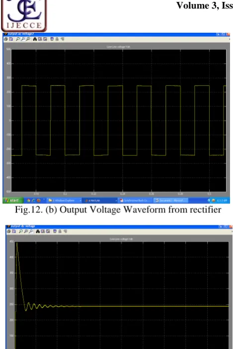
Fig.12. (b) Output Voltage Waveform from rectifier
Fig.12. (c) Final Output Voltage Waveform
Fig.13. Magnitude Plot and Phase v/s Frequency Plot The input provided at the solar input unit is 42.290V. The output obtained through the rectifier unit is shown in Figure 12(b) which is in the form of pulses as it is controlled by the pulse generator. The simulation is done using matlab in which the pulse type is time based with an amplitude of 1, and width of 50% of period.
Figure 12(c) is the final output showing the Maximum Power Point. The value of voltage has reached the value of
245.60V. The bode plot and phase-freq plot is shown clearly in Figure 13.
IV. C
ONCLUSIONThe output characteristics of photovoltaic array are non-linear and change with cell temperature and solar irradiation. Maximum Power Point Tracking control in the design of PV system is essential to draw peak power from solar array to meet the load requirements. So the efficiency, dynamic and steady-state characteristics of PV power system are chiefly influenced by the performance of MPPT controllers.
In this paper a simple Perturb and Observe Method is used. The PV output power has a direct relationship with the switching mode DC/DC converter’s switching duty ratio.
V. FUTURE SCOPE OF THE WORK
The main contribution of this thesis is tracking the maximum power point using a closed loop system consisting of some power electronic devices such as boost converter, rectifier and PV module as input device. Instead of using semiconductor devices live diodes IGBT’s are used.
In future, this approach can be applied for tracking the Maximum Power Point without using any type of controller. Hence, reducing the cost and increasing the efficiency of the system.
The basic advantage of only using Perturb and Observe method is that when it is properly optimized it can offer very high Maximum Power Point Tracking efficiency, which is highly competitive against other Maximum Power Point Tracking algorithms
R
EFERENCES[1] Ratna Ika Putri and M. Rifa’I Maximum Power Point Tracking Control for Photovoltaic System Using Neural Fuzzy, International Journal of Computer and Electrical Engineering, Vol.4, No.1, February 2012.
[2] Paper Presented on Renewable Energy Source By Rucha Korhale.
[3] PV Cells- Working Principle and Applications by Ir Dr Edward LO Associate Professor Department of Electrical Engineering The Hong Kong Polytechnic University.
[4] Steven L. Brunton, Clarence W. Rowley, Sanjeev R. Kulkarni,
Fellow, IEEE, and Charles Clarkson, Maximum Power Point
Tracking for Photovoltaic Optimization using Ripple Based Etremum Seeking Control, IEEE TRANSACTIONS ON POWER ELECTRONICS, VOL. 25, NO. 10, OCTOBER 2010.
[5] Nicola Femia, Member, IEEE, Giovanni Petrone, Giovanni Spagnuolo, Member, Optimization of Perturb and Observe Maximum Power Point Tracking Method IEEE, and Massimo Vitelli IEEE TRANSACTIONS ON POWER ELECTRONICS, VOL. 20, NO. 4, JULY 2005.
[6] C. Liu, B. Wu and R. Cheung Department of Electrical & Computer Engineering, Ryerson University, Toronto, Ontario, Canada M5B 2K3, ADVANCED ALGORITHM FOR MPPT CONTROL OF PHOTOVOLTAIC SYSTEMS, Canadian Solar
International Journal of Electronics Communication and Computer Engineering Volume 3, Issue 4, ISSN (Online): 2249–071X, ISSN (Print): 2278–4209
[7] Dezso Sera, Student Member, IEEE, Remus Teodorescu, Senior
Member, IEEE, Jochen Hantschel, and Michael Knoll,
Optimized Maximum Power Point Tracker for Fast-Changing Environmental Conditions, IEEE TRANSACTIONS ON INDUSTRIAL ELECTRONICS, VOL. 55, NO. 7, JULY 2008. [8] D. P. Hohm and M. E. Ropp*,y Electrical Engineering
Department, South Dakota State University, Brookings, SD 5700-2220, USA, Comparative Study of Maximum Power Point Tracking Algorithms, PROGRESS IN PHOTOVOLTAICS: RESEARCH AND APPLICATIONS Prog. Photovolt: Res. Appl. 2003; 11:47–62 (DOI: 10.1002/pip.459).
[9] Mohamed Salhi1, and Rachid El-Bachtiri, A Maximum Power Point Tracking Photovoltaic System using a Proportional Integral Regulator, Science Academy Transactions on Renewable Energy Systems Engineering and Technology (SATRESET) Vol. 1, No. 2, June 2011 ISSN: 2046-6404. [10] Mohamed Azab, A New Maximum Power Point Tracking for
Photovoltaic Systems, World Academy of Science, Engineering and Technology 44 2008.
[11] Tamer T.N. Khatib National University of Malaysia, Department of Electrical Electronic & System Engineering Bangi 43600, Selangor, Malaysia, A New Controller Scheme
for Photovoltaics Power Generation Systems, European
Journal of Scientific Research ISSN 1450-216X Vol.33 No.3 (2009), pp.515-524©EuroJournalsPublishing,Inc.2009.
A
UTHOR’
SP
ROFILESonali Surawdhaniwar
was born in Nagpur,in 1987. She received the Bachelor of Engineering Degree in Electronics and Telecommunication from CSVTU University,Chhattisgarh in the year 2009.
International Journal of Electronics Communication and Computer Engineering Volume 3, Issue 4, ISSN (Online): 2249–071X, ISSN (Print): 2278–4209
[7] Dezso Sera, Student Member, IEEE, Remus Teodorescu, Senior
Member, IEEE, Jochen Hantschel, and Michael Knoll,
Optimized Maximum Power Point Tracker for Fast-Changing Environmental Conditions, IEEE TRANSACTIONS ON INDUSTRIAL ELECTRONICS, VOL. 55, NO. 7, JULY 2008. [8] D. P. Hohm and M. E. Ropp*,y Electrical Engineering
Department, South Dakota State University, Brookings, SD 5700-2220, USA, Comparative Study of Maximum Power Point Tracking Algorithms, PROGRESS IN PHOTOVOLTAICS: RESEARCH AND APPLICATIONS Prog. Photovolt: Res. Appl. 2003; 11:47–62 (DOI: 10.1002/pip.459).
[9] Mohamed Salhi1, and Rachid El-Bachtiri, A Maximum Power Point Tracking Photovoltaic System using a Proportional Integral Regulator, Science Academy Transactions on Renewable Energy Systems Engineering and Technology (SATRESET) Vol. 1, No. 2, June 2011 ISSN: 2046-6404. [10] Mohamed Azab, A New Maximum Power Point Tracking for
Photovoltaic Systems, World Academy of Science, Engineering and Technology 44 2008.
[11] Tamer T.N. Khatib National University of Malaysia, Department of Electrical Electronic & System Engineering Bangi 43600, Selangor, Malaysia, A New Controller Scheme
for Photovoltaics Power Generation Systems, European
Journal of Scientific Research ISSN 1450-216X Vol.33 No.3 (2009), pp.515-524©EuroJournalsPublishing,Inc.2009.