University of East London Institutional Repository: http://roar.uel.ac.uk
This paper is made available online in accordance with publisher policies. Please scroll down to view the document itself. Please refer to the repository record for this item and our policy information available from the repository home page for further information.
To see the final version of this paper please visit the publisher’s website. Access to the published version may require a subscription.
Author(s):
Lota, Jaswinder. Al-Janabi, Mohammed., Kale, IzzetArticle Title:
Nonlinear-Stability Analysis of Higher Order ∆–Σ Modulators for DC and Sinusoidal Inputs.Year of publication:
2008Citation:
Lota, J. Al-Janabi, M., Kale, I. (2008) ‘Nonlinear-Stability Analysis of Higher Order ∆–Σ Modulators for DC and Sinusoidal Inputs’IEEE Transactions on Instrumentation and Measurement 57 (3) 530-542Link to published version:
(not available)DOI:
(not stated)Publisher statement:
Nonlinear-Stability Analysis of Higher Order
∆
–
Σ
Modulators for DC and Sinusoidal Inputs
Jaswinder Lota,
Member, IEEE
, Mohammed Al-Janabi,
Member, IEEE
, and Izzet Kale,
Member, IEEE
Abstract—The present work that exists on predicting the sta-bility of ∆–Σ modulators is confined to DC input signals and unity quantizer gains. This poses a limitation for numerous∆–Σ
modulator applications. The proposed research work gives the stability curves for DC, sine, and dual sinusoidal inputs for any value of the quantizer gain. The maximum stable input limits for third-, fourth-, and fifth-order Chebyshev-Type-II-based∆–Σ
modulators are established using the describing-function method for DC and sinusoidal inputs. Closed-form mathematical expres-sions for the gains of the quantizer for higher order∆–Σ modu-lators whose inputs are two concurrent sinusoids are derived from first principles. The derived stability curves are shown to agree reasonably well with the simulation results for different types of input signals and amplitudes.
Index Terms—DC and sinusoidal inputs, nonlinear, quantizer gain, stability,∆–Σmodulators.
I. INTRODUCTION
T
HE WELL-KNOWN sources of nonlinearity in ∆–Σmodulators are the 1-bit quantizer, op-amp nonlinear DC gain, op-amp slew rate, and nonlinear switch response. The nonlinear op-amp gain and slew rate result in considerable harmonic distortion at the output spectrum of the∆–Σ mod-ulator. The nonlinear quantizer affects the stability of the∆–Σ
modulator and is therefore the main area of investigation in this paper. The stable input amplitude limits for∆–Σmodulators are complicated to predict due to the severe nonlinearity of the 1-bit quantizer. To date, various approaches have been applied to more accurately characterize the quantizer [1]–[6], [8], [9]. One technique is to model the quantizer as a threshold function in the state equations. The analysis, however, gets complicated for higher order∆–Σmodulators and has therefore been limited to the first- and second-order ∆–Σ modulators [1]–[4]. For higher order∆–Σmodulators, linearized modeling is a method that has been found to be useful for performance analysis [5], [6], [8], wherein the 1-bit quantizer is modeled as a linear gain and an additive noise source. However, apart from performance predictions, the linearized-modeling approach did not previously provide useful stability predictions until a new
Manuscript received January 16, 2007; revised June 14, 2007.
J. Lota and M. Al-Janabi are with the Applied DSP and VLSI Re-search Group, Department of Electronics, Communications, and Software Engineering, University of Westminster, W1B 2UW London, U.K. (e-mail: [email protected]; [email protected]).
I. Kale is with the Applied DSP and VLSI Research Group, Department of Electronic Systems, University of Westminster, W1B 2UW London, U.K. and also with the Applied DSP and VLSI Research Centre, Eastern Mediterranean University, Gazimagusa, Mersin 10, N. Cyprus (e-mail: [email protected]).
Color versions of one or more of the figures in this paper are available online at http://ieeexplore.ieee.org.
[image:2.594.341.520.173.238.2]Digital Object Identifier 10.1109/TIM.2007.911640
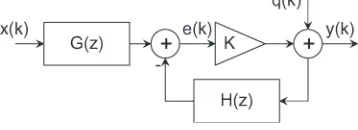
Fig. 1. Quasi-linear∆–Σmodulator quantizer model.
interpretation of the instability mechanism for∆–Σmodulators based on the noise-amplification curve was given in [9]. This is however restricted for DC inputs and unity quantizer gains. This quasi-linear method can be extended to more than one input with each input represented by a separate equivalent gain. This concept forms the basis for the describing-function (DF) method [10]. In this paper, the stability analysis based on the noise-amplification curve is accomplished using the DF method for DC single- and dual-tone sinusoidal inputs for nonunity quantizer-gain values. The noise transfer functions (NTFs) of these ∆–Σ modulators utilize Chebyshev-Type-II filters because they achieve better in-band signal-to-noise ra-tios (SNRs) as compared with Butterworth filters of the same order. In Section II, the quasi-linear stability analysis of∆–Σ
modulators is explained based on the noise-amplification curve. In Section III, the derivation of the noise-amplification curves for DC and sinusoidal inputs with the DF method is given. The simulation results are illustrated and discussed in Section IV followed by the conclusions in Section V.
II. QUASI-LINEAR-STABILITYANALYSIS OF∆–ΣMODULATORS
A generic∆–Σmodulator having its quantizer replaced by a gain factorK, followed by additive quantization noiseq(k)[9], is shown in Fig. 1.
The output of the modulator in thez-domain is given by
Y(z) =STF(z)X(z) +NTF(z)Q(z) (1)
where Y(z), X(z), and Q(z) are the {z}-transforms of the output, input, and quantizer noise signals, respectively. The STF(z) and NTF(z) represent the signal transfer functions (STFs) and NTFs of the ∆–Σ modulator, which are derived from Fig. 1
STF(z) = KG(z)
1 +K·H(z) (2)
NTF(z) = 1
1 +KH(z). (3)
Fig. 2. A(K)curves for some Chebyshev-Type-II NTFs.
It can be seen from (2) and (3) that the poles of the denom-inator[1 +KH(z)] determine the stability of the modulator. For a given loop-filter H(z), there will be a certain interval
[Kmin, Kmax]for which the modulator is stable [11]. Assuming
q(k) to be Gaussian white noise G(0, σ2
q) and the transfer function betweenq(k)andy(k)to be known, then the output noise variance is given by [9]
Var{y(k)}=σq2
1
0
NTF(ejπf)2df =σq2A(K) (4)
where σ2q is the variance of q(k) andA(K)is the total out-put noise-power-amplification factor. Using Parseval’s relation,
A(K)can be found in the time-domain as
A(K) = ∞
k=0
|NTF(k)|2 ∆=NTF22 (5)
where NTF(k) is the impulse response corresponding to NTF(z)andA(K)is the squared second-norm of NTF(z)[9]. TheA(K)curves of the loop-filter are crucial for the stability analysis of∆–Σmodulators. Typical curves for the Chebyshev-Type-II NTFs are shown in Fig. 2.
The Amin value is the global minimum of the curve. IfK
increases slightly in the region, whereA(K)is monotonically increasing, it results in a higher A(K) value, which leads to more quantization noise transfer into the∆–Σmodulator. This tends to decreaseK, leading to a stable equilibrium state [9]. However, where theA(K)curve is monotonically decreasing, even small perturbations can destabilize the modulator. As the signal power increases, the values along theA(K) curve decrease and approachAmin. The two values ofKcome close
together and, finally, merge at Amin. This characterizes the
onset of instability. The modulator-operating region escapes to the left portion of the curve, where it is characterized by low values ofK. Therefore, for stable operationA(k)> Amin[9].
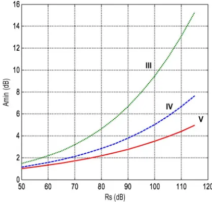
The Amin values for the Chebyshev-Type-II-based NTFs are
[image:3.594.319.528.69.268.2]shown in Fig. 3.
Fig. 3. Aminvalues versus stop-band attenuation for the third-, fourth-, and
[image:3.594.337.515.308.376.2]fifth-order Chebyshev-Type-II-based NTFs.
Fig. 4. ∆–Σmodulator linear-signal model.
Fig. 5. ∆–Σmodulator linear-noise model.
III. NOISE-AMPLIFICATIONCURVES—DF METHOD
Using the DF model, the quantizer-gain Kshown in Fig. 1 can be represented with two separate gainsKxandKn[6], as shown in Figs. 4 and 5.
Fig. 4 describes the model for the input signal with linear gainKx, whereas Fig. 5 describes the noise-signal model with linear gainKn. The combined output signal is given by
y(k) =yx(k) +yn(k). (6)
A. DC Input
The linearized gains for a 1-bit quantizer with an output±∆
have been calculated in [6] and are given as follows, where
erf(·)is the error function [7]
Kn= 2
∆ σ2
en
e−m2e/2σen2 (7)
Kx=
∆ me
erf
me
σen √
2
wheremeis the mean value of the quantizer input in the signal model, andσ2
en is the noise variance input to the quantizer in the noise model. The variance of the output signal is given by
Var{y(k)}=Ey2(k)−E2{y(k)} (9)
whereE{·}is the expectant operator.
The output signal in the time domain can be expressed as
y(k) =en(k)Kn+q(k) +ex(k)Kx. (10)
The first term on the right-hand side of (9) is the power of the output signal, which is given by
Ey2(k)=Ee2n(k)Kn2+Eq2(k)+Ee2x(k)Kx2
(11)
Ey2(k)=σ2enKn2+σq2+m2eKx2. (12)
Since the quantization noise is assumed asG(0, σq2)the mean values ofen(k)andq(k)are equal to zero, then the second term on the right-hand side of (9) becomes
E2{y(k)}=m2eKx2. (13)
The resultant variance of the output signal using (9), (12), and (13) becomes
Var{y(k)}=σen2 Kn2+σq2. (14)
The noise-power-amplification factor for a DC input signal
Adc(K)after using (4), (7), and (14) simplifies to
Adc(K) =
Var{y(k)} σ2
q
=
2
π
e−λ22
+σ2
q
σ2
q
(15)
whereλis a factor defined as follows:λ=me/σen √
2, andσq2 is the quantization noise power given by [6]
σ2q = ∆2
1−mx ∆2 −
2 πe
−2[erf−1(mx
∆ )] 2
. (16)
B. Sinusoidal Input
The linearized gains for a sinusoidal input and random Gaussian feedback components have been solved for the case of an ideal relay in [12], which can be assumed for a 1-bit quantizer with an output of±∆[6] and are shown as follows:
Kn=
2 π
1
2 ∆
σen
F
1 2,1,−υ
2
(17)
Kx=
2 π
1
2 ∆
σen
F
1 2,2,−υ
2
. (18)
Here,υ∆(a/√2) = (1/σen), where ais the amplitude of the sinusoidal input signalx(k). The expressionF(α, γ, x)is the
confluent hypergeometric function defined by [13], andΓis a gamma function [7]
F(α, γ, χ)∆= 1 +αχ
γ +
α(α+ 1)χ2
γ(γ+ 1)Γ2+· · · (19)
The variance of the output signal is given by
Var{y(k)}=Ey2(k)−E2{y(k)}. (20)
The power of the output signal is given by
Ey2(k)=Ee2n(k)Kn2+Eq2(k)+Ee2x(k)Kx2
(21)
Ey2(k)=σen2 Kn2+σ2qs+σex2 Kx2 (22)
whereσqs2 is the quantization noise power for a sinusoidal input. The second term on the right-hand side of (20) is
E2{y(k)}=E2{en(k)Kn}+E2{q(k)}+E2{ex(k)Kx}
(23)
E2{y(k)}=E2{ex(k)}Kx2 (24)
where the mean values ofen(k)andq(k)are zero. The input signal is a sinusoid modeled as a random variable (RV) having constant amplitude. Since the phase is random with a uniform probability density function (pdf) E{ex(k)}= 0. Therefore, from (20) and (24)
Var{y(k)}=Ey2(k). (25)
Given that the frequency of x(k) is small in the baseband region, this then results in [6]
Ex(z)
X(z) ≈ 1 Kx
. (26)
The variance ofex(k)is
σex2 = 1 K2
x
σ2x. (27)
From (25) and (27), the output-signal variance is
Var{y(k)}=σqs2 +Kn2σ2en+σx2. (28)
The output-noise variance is therefore
Varn{y(k)}=σqs2 +Kn2σ2en. (29)
Substituting (17) in (29), the noise-amplification factor for a sinusoidal input signal becomes
Asine(K) =
2
π F
21 2,1,−υ
2
+σqs2
σ2
qs
The values of υ and σ2
qs can be found using the following expressions derived in [6]:
υ2F2
1 2,2,−υ
2 =π 4 a2 ∆2 (31)
σqs2 = ∆2
1− a
2
2∆2 −
2 πF
2
1 2,1,−υ
2
. (32)
C. Two Sinusoidal Inputs (Incommensurate)
The linearized gains for two sinusoidal input signals
xa(t) =acos(w1t+φ1),xb(t) =bcos(w2t+φ2)and a
ran-dom Gaussian signal representing the feedback components have been solved for the case of the 1-bit quantizer, as shown in the Appendix, where the final expressions are given by
Ka=
2 π
5
2∆
σ b a 1 1 2−ρ2b
1F1
1,3 2,−ρ
2 a +ψa (33)
Kb=
2 π
5
2∆
σ
a
b
1
1 2−ρ2a
1F1
1,3 2,−ρ
2
b
+ψb
(34)
Kn=
2 π ∆ σ
e−ρ2ae−ρ2bζ (35)
where
ψa=
4 3ρ 2 a− 16 45ρ 4 a+ 16 175ρ 6 a− 128 6615ρ 8
a+· · ·
(36)
ψb=
4 3ρ 2 b− 16 45ρ 4 b+ 16 175ρ 6 b− 128 6615ρ 8
b+· · ·
(37)
ζ=
1 +ρ2aρ2b+ρ
4
aρ4b
4 +
ρ6aρ6b 36 +
ρ8aρ8b 576 +· · ·
(38)
andρ2
a= (1/2)(a2/σ2);ρ2b = (1/2)(b2/σ2). From (29), the output-noise variance is given by
Var{y(k)}=σen2 Kn2+σ2qab (39)
whereσ2qab is the quantization noise power for the two uncor-related sinusoidal inputsxa(t)andxb(t). Therefore, from (35) and (39), the noise-amplification factor is given by
Aab(K) =
2
π
e−ρ2
ae−ρ2b
2
ζ2+σ2
qab
σ2
qab
. (40)
Sincexa(t)andxb(t)are uncorrelated, the power of the output signal is given by
Ey2(k)=σen2 Kn2+σqab2 +σ2ebKb2+σ2eaKa2 (41)
whereσ2
ebandσ2eaare the powers of the sinusoidal inputs at the quantizer input. From (27), we have
σeb2 = 1 K2
b
σb2
σea2 = 1 K2
a
σa2. (42)
From (35), (41), and (42), we get
∆2= 2 π∆
2{e−ρ2
ae−ρ2b}2ζ2+σ2 qab+
b2 2 +
a2
2 . (43)
Rearranging (43), the quantization noise power is given by
σ2qab = ∆2
1− a
2
2∆2 −
b2
2∆2 −
2 π
e−ρ2ae−ρ2b
2
ζ2
. (44)
From (34) and (42), we get
2 π 5 a2 b2 ρ2 b 1 2−ρ2a
2
1F1
1,3 2,−ρ
2
b
+ψb
2
= b
2
2.
(45)
Similarly, from (33) and (42) for the sinusoidxa(t), we have
2 π 5 b2 a2 ρ2 a 1 2−ρ
2
b
2
1F1
1,3 2,−ρ
2
a
+ψa
2
=a
2
2 .
(46)
The two simultaneous (45) and (46) were solved by deploying the MATLAB Symbolic Toolbox in order to get the values of
ρaandρbfor various values ofaandb.
In Sections I–III, we have seen that the noise-amplification factor can be determined in two ways, viz., statistically and nu-merically. Statistically, it can be derived from (4), provided that the noise and signal quantizer gains are known. The quantizer gain is therefore split up as signal and noise quantizer gains using the DF method. The derived noise-amplification factor here is a function of the signal amplitude and the quantization noise power. In case the of DC and single-sine inputs, the signal and noise gains have been used from the nonlinear-control theory. Equations (15) and (30) give the statistically derived noise-amplification factor for DC and single-sine inputs. For the dual sinusoidal input, the quantizer gains have been derived from the Appendix. The noise-amplification factor is arrived from (40).
The noise-amplification factor can also be derived numer-ically from (3) and (5). Here, the parameter is a function of the quantizer gain and the NTF, as shown in Fig. 2. TheAmin
value is the global minimum value of the curve. To ensure stability, the value of the noise-amplification factor must always exceed Amin. Therefore, from the statistically derived
noise-amplification factor (which is a function of the input signal and noise power), we can infer the values of the input amplitude, for which its noise-amplification factor is always greater than
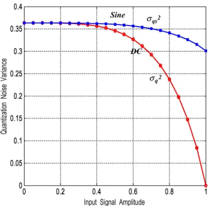
Fig. 6. Quantization noise for DC and sinusoidal inputs.
Fig. 7. Variation ofυ(sine) andλ(DC) versus the input-signal amplitude.
particular NTF. The derived stability curves for a given NTF can therefore be plotted and will be covered in the next section.
IV. RESULTS ANDSIMULATIONS
A. DC and Single Sinusoidal Inputs
The variation of the DC and sinusoidal-input quantization noise powerσ2
q andσqs2, with respect to the input-signal am-plitude using (16) and (32), are shown in Fig. 6.
As shown,σq2decreases and becomes zero as the input-signal amplitude increases to unity. The quantization noise power
σqs2 does not decrease to zero and remains at 0.3 for an input amplitude of 1.0. Equation (31) has been solved forυup to the tenth power ofυusing the MATLAB Symbolic Toolbox.
Fig. 7 shows the variation of λandυ, with respect to the input-signal amplitude.
[image:6.594.46.292.307.532.2]Fig. 8. Noise-amplification factor for sinusoidal and DC inputs.
Fig. 9. Stable-input amplitude for Chebyshev-Type-II NTF(z).
It has been observed that, for amplitudes less than 0.4, the quantization noise λand υ are almost the same for DC and sinusoidal inputs. This coincides with the fact that, in nonlinear feedback systems, the effective gain of the nonlinearity on a small signal is independent of the signal type [10]. The noise-amplification factorsAdc(K)andAsin(K)using (15) and (30)
are shown in Fig. 8. It is shown that the values ofAdc(K)using
the DF method are the same as in [9].
Using Adc(K) and Asin(K), the maximum stable input
amplitudes for the third-, fourth-, and fifth-order Chebyshev-Type-II-based∆–Σmodulator are shown in Fig. 9.
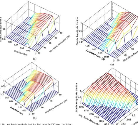
However, these are true for unity values of quantizer gainK. The variations of the stable sinusoidal input amplitude for the third-, fourth-, and fifth-order Chebyshev-Type-II-based∆–Σ
[image:6.594.306.553.310.544.2]Fig. 10. (a) Stable amplitude limit for third order for DC input. (b) Stable amplitude limit for fourth order for DC input.
attenuation are shown in Fig. 10(a) and (b) for a DC input and in Fig. 11(a) and (b) for a sinusoidal input, respectively.
For comparison, the stable input-amplitude variation for dc and sinusoidal inputs for a fifth-order Chebyshev-Type-II-based
∆–Σmodulator with a stop-band attenuation of 67 dB is shown in Fig. 12.
B. Two Sinusoidal Inputs
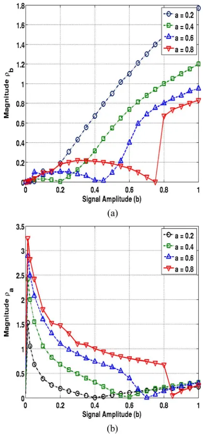
From (45) and (46), the values of ρb have been shown in Fig. 13(a). It is shown thatρb gets bigger as the amplitude b increases. However, the increase inρb gets attenuated as the signal amplitude a increases from 0.2 to 0.8. As shown, the effect of this attenuation decreases whenb > a. This becomes more noticeable fora= 0.8.
The amplitude of ρa, as shown in Fig. 13(b), is seen to gradually decrease asbincreases. It is also seen to drop sharply when the amplitude ofbbecomes greater thana.
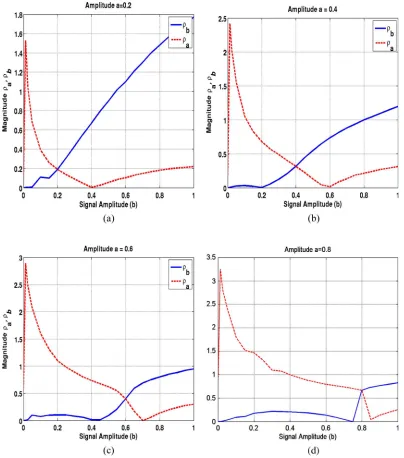
[image:7.594.42.286.69.469.2]The values ofρa andρb for the following amplitudes are as follows:a= 0.2,0.4,0.6,and0.8are shown in Fig. 14(a)–(d).
Fig. 11. (a) Amplitude limit for third order for sinusoidal input. (b) Amplitude limit for fourth order for sinusoidal input.
The magnitudes of ρa andρb become equal when both sinu-soids have the same amplitudes, i.e.,a=b.
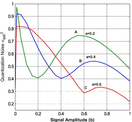
Using (44), the quantization noise power σ2
qab is plotted in Fig. 15. Theσ2
qabin the regionsb <0.2,b <0.4, andb <0.6 for the curves A(a= 0.2), B(a= 0.4), and C(a= 0.6)(left side of the nulls for the three curves), respectively, increases mainly due toρa. As ρa becomes bigger when the amplitude
aincreases from 0.2 to 0.6 in Fig. 13(b), so doesσ2
qab in this region. The increase inσ2
qabin the regionsb >0.2,b >0.4, and
b >0.6(right-hand side of the three nulls) for the curves A, B, and C, respectively, is mainly attributed toρb. Asρbincreases with a reduction in the amplitudeafrom 0.6 to 0.2 in Fig. 13(a), so doesσqab2 .
Since the quantization noise power σ2
[image:7.594.258.541.70.522.2]Fig. 12. Stable amplitude variation for DC and sinusoid inputs.
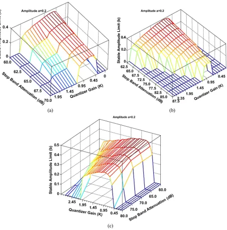
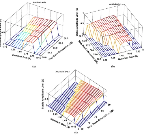
Using the values obtained forAab(K), the stable amplitude limits for b have been plotted for the third-, fourth-, and fifth-order Chebyshev-Type-II-based NTF fora= 0.2 and0.4
in Figs. 17(a)–(c) and 18(a)–(c), respectively.
Simulations for the fifth-order Chebyshev-Type-II-based
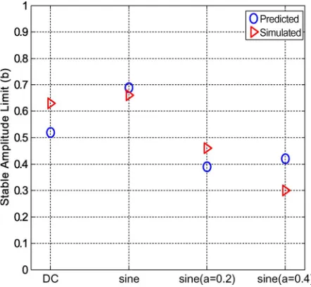
∆–Σmodulator, as shown in Fig. 19, were performed for 1400 samples, where the input amplitude was increased in steps of 0.1. The maximum stable amplitude limits were obtained and compared with simulations as shown in Fig. 20.
The difference between the theoretical and simulated input stability limits is attributed to the presence of more spectral tones when the input to the ∆–Σmodulator is a DC signal. This discrepancy in the values is seen to decrease noticeably for single-tone sinusoidal inputs, because the quantization noise in this case tends to become more Gaussian. For∆–Σmodulators whose inputs comprise of two sinusoids, the theoretical and simulated input stability limits are seen to be quite similar for relatively small input-amplitude signals. However, the differ-ence increases as the amplitudes of the two sinusoids become larger. This is due to the occurrence of tones as the ∆–Σ
modulator approaches its stability limit. A further reason for this discrepancy could be that the derivation of the three gains (i.e., two sinusoids and one Gaussian) is based on the modified nonlinearity concept. In order to compute the gain for any of the three inputs, it is assumed that the nonlinear function has been modified in turn by each of the two remaining inputs. However, in real-life, this may not be the case as all the three inputs coexist simultaneously.
V. CONCLUSION
The maximum stability input limits for different types of in-put signals and amplitudes were derived from the first principles and shown to be dependent on the quantizer gain as well as the stop-band attenuation of the NTFs. The derived stability curves were shown to depend on the noise-amplification factor,
Fig. 13. (a) Variation ofρbversusbfor differentaamplitudes. (b) Variation
ofρaversusbfor differentaamplitudes.
and therefore, the composition of the quantization noise of the∆–Σmodulators. The theoretically derived stability curves were shown to agree reasonably well with the simulation results for various types of input signals and amplitudes. The stability limits for the sinusoidal-input signals were theoretically proved to be greater than the DC case for ∆–Σ modulators of the same order. This finding is particularly useful for the design of higher order∆–Σwith improved SNRs and dynamic ranges. The derived stability curves will enable the designer of∆–Σ
modulators to predict with greater accuracy the stability of∆–Σ
modulators for any NTF and quantizer gain values.
APPENDIX
[image:8.594.45.293.69.283.2]Fig. 14. (a) Variation ofρaandρbwith amplitudebata= 0.2. (b) Variation ofρaandρbwith amplitudebata= 0.4. (c) Variation ofρaandρbwith
amplitudebata= 0.6. (d) Variation ofρaandρbwith amplitudebata= 0.8.
If the inputs to the nonlinearity are of different pdfs or of dif-ferent magnitudes of similar waveforms, the output component from one of these inputs depends not only on the magnitude of this particular input but also on the magnitudes of all the other inputs. The concept used here is the modified-linearity concept [14], whereby to determine the response to a particular input, the nonlinear characteristic is modified in turn by each of the input signals present to obtain a modified nonlinearity to which the input is applied.
The two sinusoidal inputs considered here are xa(t) =
acos(w1t+φ1) and xb(t) =bcos(w2t+φ2), where a and
b are constants, ω1 and ω2 are the sinusoidal frequencies,
assumed to be incommensurate, andφ1 andφ2 are RVs each
having a uniform pdf in the interval [0,2π]. The third input is the quantization noise assumed to be GaussianG(0, σ), i.e., with zero mean and varianceσ2.
Sinusoidal Gains
The modified nonlinearity of a 1-bit quantizer with a random input is given by [12]
n1(γ) = 2∆
γ
0
q(y)dy (A1)
where ±∆is the output of the 1-bit quantizer, andq(y)is the pdf of the random input.
Therefore, for a Gaussian input
n1(γ) = 2∆
γ
0
1 σ√2π
e−y
2
Fig. 15. Variation of quantization noise versus the two sine amplitudes.
Fig. 16. Aab(k)variation versus the two sine amplitudesaandb.
which, when integrated, simplifies to
n1(γ) = ∆erf
γ σ√2
. (A3)
Next, we consider the nonlinearityn1(γ)that is further
mod-ified ton2(γ)by one of the sinusoidal signals, for example,
xa(t). This further modified nonlinearity is given by [14]
n2(γ) =
a
−a
p(x)n1(x+γ)dx (A4)
wherep(x)is the pdf ofxa(t), i.e.,
n2(γ) =
a −a 1 π 1 √
a2−x2∆erf
x+γ σ√2
dx (A5)
can be rewritten as
n2(γ) =
2∆ π a 0 1 √
a2−x2erf
x+γ σ√2
dx. (A6)
When integrating (A6), we get (A7), which is
n2(γ) =
e−(γ2+σx2)2σ
2
π+ (γ+x)erf
x+γ σ√2
−
σ
2xerfx+γ σ√2
(a2−x2) ×
(a2−x2)3 2
(a2x2)(a2+xγ)−σ2a2−2x2σ2 a 0 . (A7)
After applying the limits, (A7) simplifies to
n2(γ) =
2∆ π
a σ2−a2
$
σ
2 πe
−γ2
2σ2 +γerf
γ σ√2
%
(A8)
where n2(γ) is now the nonlinearity of the 1-bit quantizer,
which has been modified by the sinusoidal input xa(t) and the quantization noiseG(0, σ). The next step is to evaluate the gain forxb(t)to this modified nonlinearity. This gain forxb(t) would be a function of the input amplitudesaandband would also depend on the quantization noise powerσ2.
The gainKbof the sinusoidal inputxb(t)to this nonlinearity
n2(γ)is given by [12]
Kb=
1 σ2 b b −b
xn2(x)r(x)dx (A9)
whereσ2
b =b2/2is the variance, andr(x)is the pdf ofxb(t). From (A8) and (A9), we get the gain for xb(t) as in (A10), which is
Kb =
2 b2 2∆ π2 2a σ2−a2
× σ 2 π b 0
e−x
2 2σ2 √ x
b2−x2dx
+ b 0 x2 √
b2−x2erf
x σ√2
dx
Fig. 17. (a) Stable input limits of amplitudebof third order fora= 0.2. (b) Stable input limits of amplitudebof fourth order fora= 0.2. (c) Stable input limits of amplitudebof fifth order fora= 0.2.
By putting x=bu1/2, the first integral in (A10) can be
simplified to
I1=
b
0
e−x
2 2σ2 √ x
b2−x2dx=
b 2
1
0
e−ρ2buu0(1−u)
1 2du
(A11)
where ρ2
b =b2/2σ2. This reduces (A11) to the integral form of the confluent hypergeometric function 1F1(α, β, λ), which
is [13]
Γ(β) Γ(α)Γ(β−α)
1
0
eλuuα−1(1−u)β−α−1du=1F1(α, β, λ).
(A12)
From (A11) and (A12),I1can be integrated as
I1=
b 2
1
0
e−ρ2buu0(1−u)
1 2du=b
1F1
1,3 2,−ρ
2
b
.
(A13)
The second integral in (A10) can be solved by expanding the error function and integrating within the limits, as shown in (A14)
I2=
b
0
erf
x σ√2
x2
√
b2−x2dx= 2
b2
√
Fig. 18. (a) Stable input limits of amplitudebof third order fora= 0.4. (b) Stable input limits of amplitudebof fourth order fora= 0.4. (c) Stable input limits of amplitudebof fifth order fora= 0.4.
whereηis an infinite series given by
η=
2 3ρb−
8 45ρ
3
b+
8 175ρ
5
b −
64 6615ρ
7
b+. . .
. (A15)
From (A10), (A13), and (A14), we get
Kb =
2 b2
2∆ π2
2a σ2−a2
×
$
σ
2 πb1F1
1,3 2,−ρ
2
b
+ 2 b
2
√ π
%
. (A16)
Simplifying (A16) further and rearranging the terms, the gain
Kbforxb(t)is given by
Kb=
2 π
5
2∆
σ a b
1
1 2−ρ2a
1F1
1,3 2,−ρ
2
b
+ψb
(A17)
where
ψb =
4 3ρ
2
b−
16 45ρ
4
b+
16 175ρ
6
b−
128 6615ρ
8
b+. . .
Fig. 19. Chebyshev-Type-II fifth-order modulator.
Fig. 20. Simulation results for dc, sine, and two sinusoidal inputs.
In order to obtain the gain forxa(t), we proceed as in above to get
Ka=
2 π
5
2∆
σ b a
1
1 2−ρ2b
×
1F1
1,3 2,−ρ
2
a
+ψa
. (A19)
Noise Gains
The modified nonlinearity of the first order for a Gaussian input to a 1-b quantizer is given by [12]
n(σ, γ)1=
∞
−∞
n(y+γ)H1
y
σ
q(y)dy (A20)
whereH1is the Hermite polynomial of the first order.
Substi-tuting forq(y)andn(y+γ)in (A20)
n(σ, γ)1=
∆ σ2√2π
∞
−∞ ye−y
2 2σ2dy=
2 π∆e
−γ2
2σ2. (A21)
The noise gainKnin the presence of another random input with pdfp(r)is given by [12]
Kn=
1 σ
∞
−∞
n(σ, r)1p(r)dr. (A22)
Here, we consider the additional random input as a combination of two uncorrelated sinusoidal inputs. The joint pdf p(r) of the two sinusoidal signals having amplitudes a and b, with incommensurate frequencies, is given by [15]
p(r) = r πab
1
sinθ (A23)
where
θ= cos−1
a2+b2−r2
2ab
. (A24)
From (A21), (A22), and (A23), we get
Kn=
2 π
∆ σ
a+b
a−b
e−r
2 2σ2
r
πab 1 sinθ
[image:13.594.51.272.328.532.2]
Changing the variable fromr→θ
Kn=
2 π
∆ σπ
e−a
2 2σ2e−b
2 2σ2
π
0
ekcosθdθ (A26)
wherek=ab/σ2. Solving the integral earlier, we get the noise
gain as
Kn=
2 π
∆ σ
e−ρ2ae−ρ2bζ (A27) where
ζ=
1 +ρ2aρ2b+ρ
4
aρ4b
4 +
ρ6aρ6b 36 +
ρ8aρ8b 576 +. . .
. (A28)
REFERENCES
[1] R. Schreier and W. M. Snelgrove, “Σ∆modulation is a mapping,” in
Proc. ISCAS, 1991, vol. 5, pp. 2415–2418.
[2] S. Hien and A. Zakhor, “Stability and scaling of double loopΣ∆ modu-lators,” inProc. ISCAS, 1992, vol. 3, pp. 1312–1315.
[3] H. Wang, “A geometric view ofΣ∆modulation,”IEEE Trans. Circuits Syst., vol. 39, no. 6, pp. 402–405, Jun. 1992.
[4] P. Steiner and W. Yang, “Stability analysis of the second-order Σ∆
modulator,” inProc. ISCAS, 1994, vol. 5, pp. 365–368.
[5] B. P. Agarwal and K. Shenoi, “Design methodology forΣ∆modulators,”
IEEE Trans. Commun., vol. COM-31, no. 3, pp. 360–370, Mar. 1983. [6] S. H. Ardalan and J. Paulos, “An analysis of nonlinear behavior in
delta–sigma modulators,”IEEE Trans. Circuits Syst., vol. CAS-34, no. 6, pp. 593–603, Jun. 1987.
[7] [Online]. Available: www.functions.wolfram.com
[8] K. C. H. Chao, S. Nadeem, W. L. Lee, and C. G. Sodini, “A higher order topology for interpolative modulators for oversampling A/D converters,”
IEEE Trans. Circuits Syst., vol. 37, no. 3, pp. 309–318, Mar. 1990. [9] L. Risbo, “Stability predictions for high-orderΣ∆modulators based on
quasilinear modeling,” inProc. IEEE Int. Symp. Circuits Syst., 1994, vol. 5, pp. 361–364.
[10] A. Gelb and W. E. Vander Velde,Multiple-Input Describing Functions and Nonlinear System Design. New York: McGraw-Hill, 1968. [11] E. F. Stikvoort, “Some remarks on the stability and performance of the
noise shaper or sigma–delta modulator,”IEEE Trans. Commun., vol. 36, no. 10, pp. 1157–1162, Oct. 1988.
[12] D. P. Atherton,Nonlinear Control Engineering: Describing Function Analysis and Design. London, U.K.: Van Nostrand Reinhold, 1982, pp. 383–388.
[13] A. H. Haddad, “Nonlinear systems,” inBenchmark Papers in Electrical Engineering and Computer Science, vol. 10. Dowden, Hutchinson & Ross, Inc., 1975, p. 197.
[14] D. P. Atherton and G. F. Turnbull, “Response of nonlinear characteristics to several inputs and the use of the modified linearity concept in control systems,”Proc. Inst. Electr. Eng., vol. 111, no. 1, pp. 157–164, Jan. 1964. [15] A. K. Mahalanabis and A. K. Nath, “On the dual-input describing func-tions of a nonlinear element,”IEEE Trans. Autom. Control, vol. AC-10, no. 2, pp. 203–204, Apr. 1965.
Jaswinder Lota(M’01) received the B.Sc. degree from the National Defence Academy, Pune, India, in 1987, the B.Eng. degree in electrical engineering from the Naval College of Engineering, Lonavla, India, in 1991, the M.Eng. degree in radar and communication engineering from the Indian Institute of Technology, New Delhi, India, in 1997, and the Ph.D. degree from the University of Westminster, London, U.K., in 2007.
From 1989 to 2004, he was with the Indian Navy and was last appointed as Deputy Director Systems with the Naval Headquarters, New Delhi. From 2004 to 2006, he was a research scholar with the University of Westminster. Since 2006, he has been with Sepura plc., Cambridge, U.K., as a Senior Engineer, working on developing new technologies, algorithms, standards, and techniques relevant to the future product development for TETRA-2 radio equipment. His research interests include sigma-delta modulators, digital-signal processing, radar, sonar, and telecommunication systems.
Mohammed Al-Janabi (S’98–A’00–M’04) re-ceived the B.Eng. degree (with honors) in electronic engineering and the Ph.D. degree in digital-signal processing from the University of Westminster, London, U.K., in 1993 and 2000, respectively.
He has been a Senior Lecturer with the Applied DSP and VLSI Research Group, Department of Elec-tronics, Communications, and Software Engineering, University of Westminster, since 2000. He teaches analog and digital circuit design. He also supervises projects for M.Sc. and Ph.D. degree students. His re-search interests include digital-signal processing, data converters, sigma–delta modulation, and control theory.
Dr. Al-Janabi is a chartered member of the Institute of Engineering and Technology (formerly IEE).
Izzet Kale (M’88) was born in Cyprus. He re-ceived the B.Sc. degree (with honors) in electrical and electronic engineering from the Polytechnic of Central London, London, U.K., the M.Sc. degree in design and manufacture of microelectronic systems from Edinburgh University, Edinburgh, U.K., and the Ph.D. degree in techniques for reducing digital filter complexity from the University of Westminster, London.