Design and Implementation of (72,64) Extended
Multibit SEC-DAEC Codes in FPGA
Haindavi Police1, Jaya Lakshmi Athukuri2 1, 2
Department of Electronics and Communication Engineering, Vidya Jyothi Institute of Technology
Abstract: Single error correction and Double-adjacent error correction (SEC-DAEC) codes speaks to a kind of error correction codes (ECCs) equipped for altering single and double-adjacent errors. These codes are important in applications where various adjacent errors may occur, for instance, space. ECC encoders and decoders have an even structure that makes it less demanding to place them into field-programmable gate arrays (FPGAs). This proposes techniques to develop the decoder of SEC-DAEC codes when executed in a FPGA, falling the advantage use when differentiated and the conventionalist use. This paper grows the bits and triple error cure in like manner achieved for that bits nearby SEC-DAEC codes.
Keywords: Error Correction codes (ECC), Field Programmable Gate array (FPGA), Look up Table (LUTs), Single Error Correction and Double Adjacent Error Correction (SEC-DAEC).
I. INTRODUCTION
Field-Programmable Gate Arrays (FPGAs) are even now used in different application regions, including Space and Flight [1], [2]. Their low cost and remaking limits [3] will Continue making them a Credibility for this kind of missions. Single Event Upsets (SEUs) are basic explanations behind errors in electronic devices, especially in remedial circumstances. Multiple Cell Upsets (MCUs) can occur, by this more than one bit is changed. Generally, the impacted bits are adjoining each other. There are many techniques that are made to recover the main information, when SEUs or MCUs occurs. Error Correction Codes (ECC) are one of those systems, they are extensively used in memories [4].
Linear Block Codes [5] are extraordinarily typical in view of the low thickness of the decoding equipment. Single Error Correction and Double Adjacent Error Correction (SEC-DAEC) codes have been usually used where there is no convincing motivation to address various errors. Regardless, Interleaving distance can impact an area, delay [6], which may be an issue in Embedded memories. While Interleaving distance isn't applicable, Single Error Correction and Double Adjacent Error Correction (SEC-DAEC) can be used. SEC-DAEC codes have been used to verify memories [7], [8]. The structure executed in the FPGA may require the use of SEC-DAEC to all the more probable secure either the block RAMs or an external SRAM memory. The more the FPGA resource use, the Less region is wasted.
Fig1: Example of SEC-DAEC Check System.
II. EXISTING DESIGN
A. SEC-DAEC Codes
Linear codes (n, k) has a data articulation of k bits and code articulation of n bits, including n-k balance bits using a reasonable computation. These codes can be addressed by their correspondence check arrange H (with n columns and n-k rows).
Fig. 1 shows the parity-check matrix of a (22,16) bits linear code. The underlying 16 bits identify with the data bits, and the other 6 bits contrast with the correspondence check bits. The syndrome identical to the length of number of correspondence bits in the code. If the syndrome is every one of the zeros, the got word looks at to a code word, and error is present. Something different, an error occurred. For instance, looking at the matrix from Fig. 1, a confusion of 100011 matches the second portion (set apart with a jolt), so a SE is distinguished in that bit and will be modified by turning around its regard. The error is amended by changing the contrasting piece positions.
[image:2.612.184.427.298.522.2]When a matrix of 001111 is resolved, a DAE is balanced in the first and second bits as that syndrome is the XOR of the first and second columns of the matrix (101100 XOR 100011). As such, we can say that disarranges 100011 (the second area of the cross section), 001111 (XOR of the first and second portions), and 101000 (XOR of the second and third fragments) show that an error occurred in the second bit of the code word, and it must be amended. If the syndrome matches one of the equity bit positions or the XOR of two neighbouring parity columns, by then we can express that no error occurred in the data bits even with a nonzero syndrome.
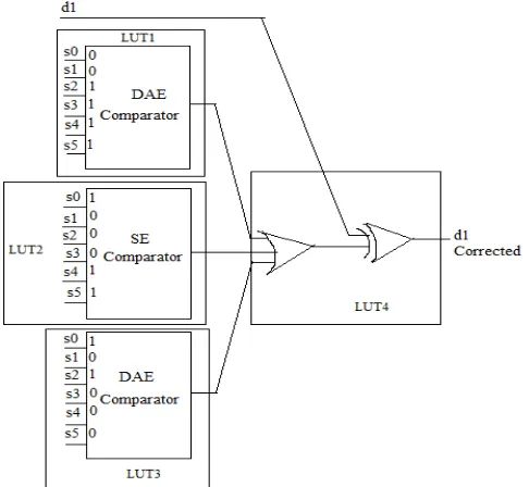
Fig 2: SEC-DAEC correction for the second bit in the (22,16) code.
The conventional circuit is showed up in Fig. 2, using the second bit of the model (d1). The syndrome bits (s0 to s5) are differentiated and the models that recognize a error in this second piece. The first and third comparators check against the DAE structures, while the second one evaluates the SE pattern. An OR gate perceives whether the comparators recognized an error. A XOR door reviews the error in the second piece (d1) if needed.
B. Basis Structure of FPGAs
FPGAs can be acclimated to unequivocal structures and changed when required as a result of their structure subject to reprogrammable method of logic blocks. Lookup tables (LUTs) are one of the sections of these method of logic blocks, used to realize the justification components of the structure. The number and characteristics of the LUTs and distinctive parts depend upon the maker and the thing family.
III. PROPOSED DESIGN
Two differentiation improvements are discussed: per-bit joined-pattern and multi bit joined-pattern correction.
A. Per-Bit Joined-Pattern Correction with Six Parity Bits
The underneath showed up. 1, is a (22, 16) code with n = 22, k = 16, and 6 uniformity bits. A syndrome identical to the XOR of two neighbouring portions implies that a DAE was recognized in the bits arranged on those column positions. The customary structure showed up in Fig. 2 can be executed into a Xilinx 7-course of action FPGA in a fundamental way, using a six-input LUT for each comparator and another LUT for the OR and XOR gates (using four data sources). To address a single piece, four differing LUTs are used, as showed up in Fig. 2. Thus, a point of confinement of 64 LUTs are required to perceive and address 16 bits, expecting no upgrade when mapping is done.
A singular LUT can be used to yield a "1" value when the bit must be redressed and "0" for the most part by checking all the models for that bit at the same time. Fig. 3 shows the most ideal approach to store up the three comparators and the OR gate of the second piece into a single six-input LUT (the third piece correction is also drawn). Likewise, the XOR gate that reviews the error has only two wellsprings of data, so a single five-input LUT (with two yields) can be used to address two bits in the meantime. Two commitments of this LUT contrast with the bits to be balanced (d1 and d2), and the others are the yields of the six-input LUTs for those bits. Along these lines, 3 LUTs would be required for every 2 bits, 24 LUTs to address the 16 data bits.
Fig 3: SEC-DAEC (22,16) per-bit joined pattern correction optimization.
B. Per-Bit Joined-Pattern Correction with Seven Parity Bits
The headway is progressively jumbled while using seven equity bits. We will next separate the (39, 32) SEC-DAEC codes, with 32 data bits and 7correspondence bits.
The standard use for (39, 32) would be Similar to the arrangement showed up in Fig. 2 for (22, 16), anyway with a fifth commitment to LUT4 contrasting with the additional piece from the syndrome (and changing the related equipment). This derives 4 LUTs are required to address each piece, up to 128 LUTs for the 32 data bits. In the veritable utilization, the fuse will play out specific enhancements, and this number will decrease. The estimation of this bit must be shared by the three instances of that data bit (the SE and the two double error syndromes). In Fig. 4, identifying with the SE structure for the eleventh piece (d10), the fifth piece is 0(0110001). Meanwhile, the DAE patterns for the eleventh piece (XOR of the abutting sections, set apart in Fig. 4) have moreover a "0" in this fifth segment (1101001 and 1010011).
An AND gate is added to check the yield of the first LUT and the typical shared estimation of s4. A NOT gate is required exactly when the ordinary estimation of the syndrome bit (s4 for this circumstance) is 0. Each segment in this structure (Fig. 4) shares something like one piece a motivating force for the three models (set apart in solid). There is a second upgrade that can be associated when a comparable piece is moved to the second LUT for two unmistakable columns. In Fig. 5, columns 11 and 13 place the fourth syndrome bit in the second LUT.
Fig 5: SEC–DAEC (39, 32) per-bit joined-pattern correction optimization for the bits d10 and d12.
Wellsprings of data are the data bits to be balanced (d10 and d12), the confusion bit that is shared by the three instances of the two segments (s4) and the yields of the first comparators. Appropriately, three LUTs are required for every two data bits to play out the cure. Hence, 48 LUTs are adequate to address the 32 data bits.
C. Multibit Joined-Pattern Correction with Six Parity Bits
Fig6: SEC-DAEC (22, 16) multi-bit joined pattern Correction for the bits d1 and d3.
Here not the second LUT can be mixed, but the first LUT, which simply has five data sources directly, can be shared by the two segments, as showed up in Fig. 6, for the second and fourth segments (d1 and d3). With this multi-bit joined-pattern correction approach, only two LUTs are used for every two bits. Looking at the matrix showed up in Fig. 1, all the columns have no short of what one piece that is shared among single and DAE plans beside the seventh one (000111, 110110, and 001001). A wary examination ought to be done to keep away from introducing errors in the conditions. With this streamlining, 7 LUTs can be emptied and the change strategy (notwithstanding the confusion tally) simply needs 17 LUTs differentiated and the 64 LUTs used in the customary design.
D. Correction with Eight Parity Bits
We can use the (72, 64) SEC-DAEC code presented in, with 64 data bits and 8 balance bits. This circumstance is logically difficult to improve as a result of these eight fairness bits. The per-bit joined-plan modification ought to even now be conceivable, anyway it must be associated with areas with two bits that can be moved to the second LUT (those that share a comparable motivating force for the three models).
E. Per-Bit Joined Correction with Eight Parity Bits
A (72,64) check matrix is used for the bit amendment. The underneath outline exhibits the (72,64) Per-bit joined change upgrade for the bits d11 and d12. By doing the Per-bit change, we can reduce the LUTs by this the region similarly diminishes. With this Optimization, 3LUTs are used to address 2 bits.
Fig8: SEC-DAEC (72,64) per-bit joined-pattern Correction for the bits d11 and d12.
F. Multi-Bit Joined-Pattern Correction with Eight Parity Bits
In the multi-bit, the triple error correction is done. By this, the 3 bits are corrected for every 8 data bits. The Look up tables (LUTs) are diminished. The layout is shown below Figure.
IV. RESULTS
Fig10: Simulation for (22,16) SEC-DAEC code
Fig11: Simulation for (22,16) Per-bit Correction
Fig12: Simulation for (39,32) Per-bit Correction
Fig13: Simulation for (22,16) Multi-bit Correction
Fig15: Simulation for (72,64) Multi-bit Correction
Table1: Comparison of SEC-DAEC (22,16), (39,32), (72,64) codes.
V. CONCLUSION
In this paper, we have acquainted a method with improve the decoders for SEC-DAEC codes in FPGAs to the extent resource use by misusing the specific characteristics of this sort of codes, and the unprecedented features fused into current FPGAs. The implementation results for three codes, a (22, 16) SEC-DAEC, a (39, 32) SEC-DAEC, and a (72,64) SEC-DAEC exhibits the proposed structures decrease the advantage utilization of the correction circuit while differentiating it and the customary plans. This diminishing can be up to 14% for the (22, 16) code, 13% for the (39, 32) code and 13% for the (72, 64). Future work will address this likelihood and the utilization of different FPGAs to consider the results and improve the headway of codes with progressively broad words.
VI. ACKNOWLEDGMENT
REFERENCES
[1] Xilinx Solutions for Aerospace & Defense Applications, accessed on Apr. 27, 2016. [Online].
[2] I. Land and J. Elliot, (2009) “Architecting ARINC 664, Part 7 (AFDX) solutions,” Xilinx, Inc., San Jose, CA, USA, Appl. Note XAPP1130 (v1.0.1), accessed on Apr. 27, 2016.
[3] B. Fiethe, H. Michalik, C. Dierker, B. Osterloh, and G. Zhou, “Reconfigurable system-on-chip data processing units for space imaging instruments,” in Proc. Design, Autom. Test Eur. Conf., vol. 1. 2007, pp. 1–6.
[4] C. L. Chen and M. Y. Hsiao, “Error-correcting codes for semiconductor memory applications: A state-of-the-art review,” IBM J. Res. Develop., vol. 28, no. 2, pp. 124–134, Mar. 1984.
[5] S. Lin and D. J. Costello, Jr., Error Control Coding, 2nd ed. Englewood Cliffs, NJ, USA: Prentice-Hall. 2004.
[6] A.Neale and M.Sachdev, “A new SEC-DED error correction code subclass for adjacent MBU tolerance in embedded memory,” IEEE Trans. Device Mater. Rel., vol. 13, no. 1, pp. 223–230, Mar. 2013.
[7] A. Dutta and N. A. Touba, “Multiple bit upset tolerant memory using a selective cycle avoidance-based SEC-DED-DAEC code,” in Proc. 25th IEEE VLSI Test Symp., May 2007, pp. 349–354.
[8] 7 Series FPGAs Configurable Logic Block. User Guide, Xilinx, Inc., San Jose, CA, USA, Nov. 2014.
[9] A. H. Farrahi and M. Sarrafzadeh, “Complexity of the lookup-table Minimization problem for FPGA technology mapping,” IEEE Trans. Computer-Aided Design Integrated. Circuits Syst., vol. 13, no. 11, pp. 1319–1332, Nov. 1994.
[10] J. H. Anderson, Q. Wang, and C. Ravishankar, “Raising FPGA logic density through synthesis-inspired architecture,” IEEE Trans. Very Large Scale Integrated. (VLSI) Syst., vol. 20, no. 3, pp. 537–550, Mar. 2012.