A 0.9 V Supply OTA in 0.18 μm CMOS Technology and Its
Application in Realizing a Tunable Low-Pass Gm-C Filter
for Wireless Sensor Networks
Soolmaz Abbasalizadeh*, Samad Sheikhaei, Behjat Forouzandeh School of Electrical and Computer Engineering, University of Tehran, Tehran, Iran
Email: *[email protected]
Received October 8,2012; revised November 22, 2012; accepted November 30, 2012
ABSTRACT
A low voltage low power operational transconductance amplifier (OTA) based on a bulk driven cell and its application to implement a tunable Gm-C filter is presented. The linearity of the OTA is improved by attenuation and source de- generation techniques. The attenuation technique is implemented by bulk driven cell which is used for low supply volt- age circuits. The OTA is designed to operate with a 0.9 V supply voltage and consumes 58.8 μW power. A 600 mVppd
sine wave input signal at 1 MHz frequency shows total harmonic distortion (THD) better than −40 dB over the tuning range of the transconductance. The OTA has been used to realize a tunable Gm-C low-pass filter with gain tuning from 5 dB to 21 dB with 4 dB gain steps, which results in power consumptions of 411.6 to 646.8 μW. This low voltage filter can operate as channel select filter and variable gain amplifier (VGA) for wireless sensor network (WSN) applications. The proposed OTA and filter have been simulated in 0.18 μm CMOS technology. Corner case and temperature simula- tion results are also included to forecast process and temperature variation affects after fabrication.
Keywords: OTA; Low Voltage; Low Power; Bulk Driven; Gm-C Filter
1. Introduction
Due to the spreading market of portable electronic equip- ments, low power low voltage circuit design has become an important goal of electronic circuits industry. Many applications, like wireless sensor networks (WSNs), need low supply voltage circuits for proper operation which results in reducing their weight and increasing their bat- tery life time. In wireless sensor networks, the voltage of battery drops over time. Since the nodes in this applica- tion cannot be easily accessed in some cases, and they should operate few months or years on a single battery, they must be designed to operate under low supply volt- ages to overcome voltage drop issues.
Operational transconductor amplifier (OTA) is an im- portant building block of many analog circuits like filters, data converters, etc. This block converts input voltage to output current with a linear transformation factor. Its fast speed and bias based tunability makes this block more appropriate for analog circuits compared with conven- tional opamps, but it has a linearity limitation drawback. The linearity of the OTA is an important issue because the linearity of the overall system would be determined by this block. This issue becomes very challenging under
the low supply voltage and limited power consumption. Also, other specifications of the OTA would be affected by low supply voltage. So, novel circuit design tech- niques should be considered to improve linearity per- formances of the OTA and overcome the deterioration of its specifications.
In order to improve linearity of the OTA, many tech- niques have been reported recently, such as attenuation [1], source degeneration [2-4], nonlinear terms cancella- tion [5-10], and triode based transconductor [11-13]. In attenuation technique, the linearity improvement is a- chieved by reducing input voltage. In this technique nonlinear terms of output current is reduced by reducing input voltage. One attenuator that can be used for reduce- ing input signal is bulk driven transistor. This cell at- tenuates input signal with γ factor which is the body ef- fect coefficient and has a value between 0.2 and 0.4 [14].
In the bulk driven cell, the input signal is applied to bulk of transistor rather than its gate, and by connecting the gate to an appropriate bias voltage, the channel is formed. Since, the input signal is applied to bulk, it is not necessary to spend a part of the input voltage range to turn the transistor on and this removes the limitation that is produced by threshold voltage requirements of the transistors in low voltage designs. So, this cell can be
used in low supply voltage circuits. In fact, the bulk driven cell can improve linearity of the OTA while oper- ating with reduced supply voltages. In [15] and [16], two low voltage bulk driven OTAs are reported. However, these low voltage cells have some drawbacks. The bulk driven transconductance is 2 to 5 times smaller than that of the gate driven, based on the technology used. This issue leads to low DC gain, low gain bandwidth (GBW) and high input referred noise. Two transconductance en- hancement techniques based on positive feedback are reported in [17] to overcome low transconductance value of the bulk driven transistor.
Source degeneration is another linearity improvement technique which is implemented by adding resistance at the source terminal of the input transistors. This tech- nique increases noise factor of the OTA in trade off with linearity improvement. Tunablity of the source degener- ated OTA is also achieved with tuning of the source de- generated resistance.
In nonlinear terms cancellation technique, linearity improvement is achieved by an appropriate sum of the nonlinear terms to cancel out nonlinearity. This tech- nique is more suitable for low supply voltage circuits, because pseudo-differential architecture can be used eas- ier in this technique.
In triode based transconductor, the drain-source volt- age of input transistors, which is biased in triode region, is kept constant. As a result, a linear OTA with constant transconductance is achieved and tunability of the trans- conductance is carried out by changing the drain-source voltage of the triode transistors.
Since using these linearization techniques become very challenging under low supply voltages, some circuit design methods should be considered for low supply voltage designs. One of these methods, which is men- tioned before, is the bulk driven cell. Some other low voltage circuit design methods are flipped voltage fol- lower cell (FVF) [18], sub-threshold MOSFET [16], pseudo-differential pairs [19], and floating gate. In these methods some of the OTA’s specifications such as line- arity, noise, open loop DC gain, and unity gain band- width (UGBW) are deteriorated in trade off with reduce- ing supply voltage. So, appropriate topology and biases should be used for getting more optimized circuits.
In this work, a low voltage low power bulk driven OTA is presented. This low voltage OTA can be used for some applications such as WSNs. The proposed OTA uses attenuation and source degeneration techniques for its linearity improvement. By using bulk driven transis- tors for input pairs, linearity improvement can be achie- ved while the OTA can operate with reduced supply voltages. The proposed OTA can operate with a 0.9 V supply voltage in a 0.18 μm CMOS n-well process. In order to overcome some drawbacks of using bulk driven
transistors, such as low DC gain, low unity gain band- width, and high noise, the transconductance enhancement technique, which is reported in [17], is applied to input pairs. In [17], this technique is applied to the bulk driven transistors, too. But no other linearity improvement tech- nique is applied to input pair for further improving line- arity. In the proposed OTA, this technique is applied to source degenerated bulk driven input pair and a self- cascode structure is used for increasing output impedance and so the DC gain. Also, in this work, tuning is added to the OTA for compensating the PVT variations. Tuning of the proposed OTA is achieved by varying the source de- generated resistance, which is implemented by a transis- tor.
As an application of the proposed low voltage low power OTA, a third-order low-pass Butterworth filter is designed. This low voltage Gm-C filter acts as a channel select filter and variable gain amplifier (VGA) for some wireless sensor network applications, such as those com- pliant with IEEE 802.15.4 standard, also known as Zig- Bee. The proposed filter has a gain tuning from 5 dB to 21 dB with 4 dB gain steps.
The rest of this manuscript is organized as follows. In Section 2, the proposed OTA with circuit details is dis- cussed. Gm-C filter design and its gain tuning are de- scribed in Section 3. Section 4 shows the simulated per- formances of the OTA and filter. Some discussion about the circuit simulations are made in Section 5. Finally, the conclusions are drawn in Section 6.
2. Design of the Transconductance
2.1. Design of the Input Stage
In the bulk driven cell, input signal is applied to the bulk of input transistors rather than their gates. The bulk driven MOSFET cell acts similar to a JFET. The channel conductivity is varied by bulk-source voltage and, as a result, the bulk driven transistor can conduct with zero, negative, or slightly positive input voltage, similar to a depletion type device [20]. However, this low voltage cell has some disadvantages. The transconductance of the bulk driven transistor is much smaller than that of the gate driven, and this causes low DC gain, low gain bandwidth, and high input referred noise. Another dis- advantage of this cell is that for an n-well process, only PMOS bulk driven MOSFETs are available. In order to use NMOS bulk driven MOSFETs, deep n-well layer is needed to achieve a twin well process. To reduce cost of circuit implementation, we have used bulk driven PMOS transistors, in this paper.
for linearity improvement of the OTA, which is appro- priate for low voltage circuits. The tuning transistor, which acts as source degenerated resistance, improves linearity of the OTA and vary the transconductance value of the OTA for compensation of PVT variations. Al- though source degeneration technique, increases noise factor of the OTA, but, in trade off, can reduce third or- der harmonic distortion. When input transistors operate in strong inversion region, their drain current is ex- pressed as follows:
21 2
D p ox SG th
W
I C V V
L
(1)in which, parameters have their usual meanings and the channel length modulation is ignored for simplicity. In the bulk driven transistor, threshold voltage is described by:
0 2 2
th th F BS F
V V V (2) in which, φF is the surface potential, γ is the body effect coefficient, and Vth0 is threshold voltage when the
bulk-source voltage is zero.
By using Equations (1) and (2), the transconductance value of the input transistors, not considering the source degenerated resistance, is given by:
2 2 2
D
mb P ox D
BS F BS
I W
g C I
V V
L
(3)
By applying source degeneration technique to the in- put stage, the transconductance value is changed to:
, 1 mb mb sd mb g g g R (4)
in which, R is the half of the resistance of the source de-generated transistor. From Equation (4), it is obvious that, by varying the value of R, the transconductance tuning can be achieved. Although the source degenerated tech-nique, reduces transcondactance value by 1 + gmbR factor, but greatly reduces the third order harmonic distortion term by factor of (1 + gmbR)2. The third order harmonic distortion term of the input transistors can be calculated from Equation (1) to Equation (4), as below.
3 , 3,saturation 3 2 0 2 2 3! 2 1 116 2 2
D sat
BS
P ox F SG th
mb
F BS F BS
I HD
V
C W V V
g R
L V V
(5)
As can be seen from Equation (5), the third order har- monic distortion term is attenuated by γ and (1 + gmbR)2 factors, which are related to the bulk driven transistors and the source degeneration transistor, respectively.
2.2. Complete Design of the Proposed Transconductance
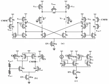
The complete OTA is demonstrated in Figure 2 which consists of the transconductance main stage, the common mode feedback circuit (CMFB), and the bias circuit. In this figure, all transistors with the same dimensions are labeled with the same symbols and the tuning transistor is labeled with SD (source degenerated).
In order to overcome the main bulk driven issue (low transconductance value), the transconductance enhance- ment technique is applied to the input pairs [17]. This technique is implemented by M1, M3, M4, M5 and M6. A
partial positive feedback which is implemented by M3,
reduces the conductance of the node A and increases gmb,sd by the factor as below.
, 3 , 4
1 1 gm M gm M
(6)
Because the overall feedback must remain negative, gm,M4 must be larger than gm,M3. In fact, by choosing
gm,M3/gm,M4 close to unity, the circuit is very prone to in-
stability, and linear input voltage range becomes small. So, proper sizing for M3 and M4 should be used to
achieve a stable circuit. The flipped voltage follower current mirror is used for mirroring current to the output.
At the output stage of the OTA, self-cascode structure, which is accomplished by M8 and M9, is used for in-
creasing output impedance. In low voltage circuits, it is not possible to stack transistors for increasing output impedance. Self-cascode structure is one solution, which is used in low voltage circuits to increase output imped- ance [21]. The self-cascode structure has much larger effective channel length and therefore much lower effect- tive output conductance. The transistor M9 in this struc-
ture is in linear region and acts as a resistor. For optimal operation of the structure, the dimension of M8 should be
kept larger than M9. The self-cascode structure is more
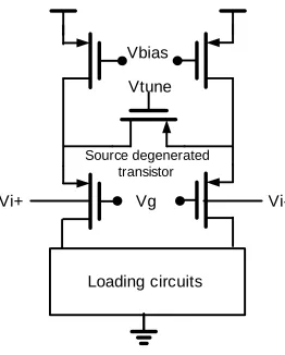
Loading circuits
Vi+ Vg
Vi-Vbias
Vtune
[image:3.595.357.488.550.713.2]Source degenerated transistor
Figure 2. The complete OTA (a) The transconductance main stage; (b) The CMFB circuit; (c) The bias circuit.
suitable for low voltage circuits compared with conven- tional cascode, as it has high output impedance similar to that of a conventional cascode, while the output voltage requirements of the self-cascode could be similar to a single transistor.
is high, the SWp and SWn switches are off and on, re- spectively. In this mode, the OTA is active and acts nor- mally. For turning of the OTA, EN signal should go low. In this mode, the SWn switches are turned off and thus no current path exists to the ground. On the other hand, the SWp switches turn on and force PMOS biases to VDD. So, PMOS transistors turn off and the OTA be- comes disabled.
Figure 2(b) shows the CMFB circuit, which sets the dc voltage of the output to Vref. In order to achieve maximum output swing, output common mode is set to VDD/2. In the CMFB circuit, the output voltage of the OTA is averaged by resistance network and is compared with Vref. The resultant signal adjusts the bias of the self-cascode structure and set the output dc voltage around Vref.
2.3. Noise in the Proposed OTA
In this section, the noise performance of the proposed OTA is studied. Since, the major part of the voltage gain of the proposed OTA is produced by the output stage, the main part of the input referred noise is generated by the input stage. So, the noise of the output stage can be ig- nored. The total input referred noise of the overall OTA, which consists of flicker and thermal noise is approxi- mated as: see Equation (7).
The bias circuit which is used to generate the proper bias voltages of the OTA is shown in Figure 2(c). In this figure, the diode connected transistors produce the fixed voltages of Vbp and Vbn for biasing of PMOS and NMOS transistors, respectively.
In Figure 2 the transistors SWn and SWp are switches for turning on and off the OTA for gain tuning of the filter (will be described in details in Section 3). When EN
In the above equation, Kf is the flicker noise parameter, K is the Boltzmann constant, T is the temperature, f is the
2 2
, 2 1 2 3 4 6
2 2 2 2
2
, 1 , 2 , 3 , 4
2 2 2 2
1 2 3 4
8
2 1
3
2 1
1
n in m mb mb m m m m
m eff
fp sat m fp sat m fn sat m fn sat m fp s
mb mb
ox m eff m eff m eff m eff
KT
V g g R g R g g g g
g
k g k g k g k g
g R g R
c f WL g WL g WL g WL g
,
k 2
6 2 6 at m
m eff g
WL g
frequency, gm,eff is η*gmb,sd and other parameters have their usual meanings. The factor of 2 is considered for the two halves of the input stage.
Based on Equation (7), although the input referred noise is increased by the noise contribution of M1 - M4
and M6, which is caused by the transconductance en-
hancement technique, the total input referred noise is reduced. In fact, by using this technique, the DC gain of the OTA enhances. Therefore, the input referred noise of the transistors not involved in this technique is reduced. Based on Equation (7), the total noise can be reduced by minimizing the gate transconductance of all transistors and the current of M6.
3. Gm-C Filter Design
The low voltage OTA, which is described in previously, can be used as channel selection filter and variable gain amplifier for the receiver of wireless sensor network ap- plications. IEEE 802.15.4 or ZigBee is one standard which is introduced for wireless sensor networks. This low power standard is deigned for control applications and wireless sensing. It is also appropriate for comer- cial uses, industrial and home automation, personal health care appliances, and many other applications. In order to satisfy requirements of these articles, the sensors of ZigBee standard should be able to operate for several months on button cells or small batteries [22]. Therefore, the circuits of sensors used in this standard should be low voltage and low power. Considering a zero-IF architect- ture for the 2.4 GHz ZigBee receiver and assuming some margins in channel selection, a third order Butterworth low-pass filter with more than 2-MHz bandwidth is needed [22]. This filter provides the requirement of 0-dB
[image:5.595.82.515.501.721.2]and 30-dB rejections at the adjacent channel (±5 MHz) and the alternate channel (±10 MHz), respectively [22]. In order to obtain some gain controlling based on the specifications of the receiver, the related filter should be able to operate as a variable gain amplifier, too.
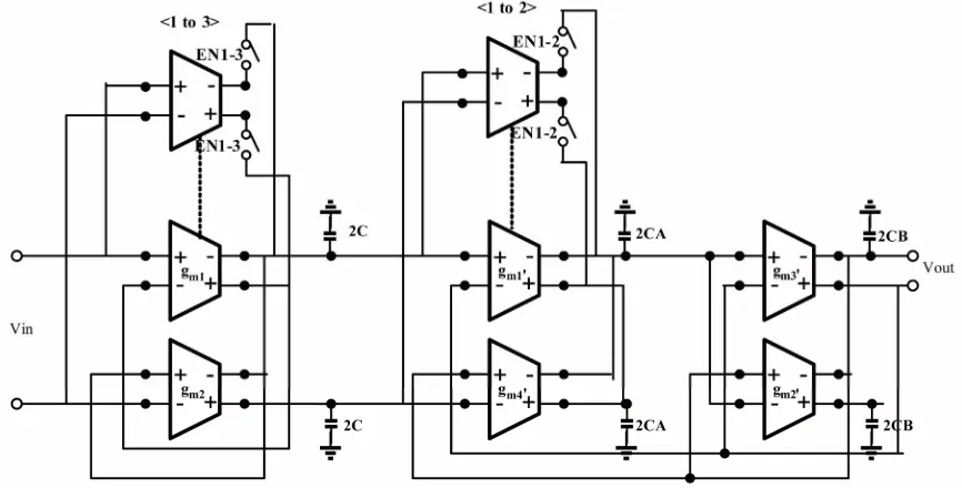
Figure 3 shows the structure of the filter designed for the ZigBee standard. The filter is implemented by cas- cade of a first-order low-pass stage and a biquad stage for realizing a complex pole pair. This structure, which is reported in [23], is more suitable for low voltage circuits compared with the conventional structure. Because this structure can increase output swing, which is reduced due to low supply voltage. Since, the current delivered to each capacitor of the filter is the same as that of the con- ventional ones, the new structure does not change the cut off frequency and quality factor of the filter. Due to re- ceiving the signal with the same amplitude and phase in both inputs of the OTA in this structure, the total voltage swing at the inputs of each transconductance is reduced compared with conventional structure and this relieves the need for a high-swing OTA.
Gain tuning of the filter can be obtained based on the fact that by increasing the number of parallel gm blocks, the transconductance value increases linearly. In fact, by tuning the resistance of the transistor used as degenera- tion, and by parallelizing the first OTA of each stage in the filter by a similar OTA, gain variation is achieved.
In Figure 3, the switches, which are controlled by EN<i> signal, are implemented by transistors. When the cotrolling signal goes high, the related OTA is activated and increases the gm value and also, gain of the filter. En<1-3> and EN<1-2> refer to the control of three and two OTAs that are placed in parallel, and can be turned
on and off individually to obtain the required gain value. The frequency response of the filter is derived as: where,
1 1 3
2
2 4 2 3
1 2
2 2
0 0
2π
m m m A B
m m A m m A B
c H S
g C g g C C
s g C s s g C g g C C
k k
s f s s Q
(8)
2 2 2 2
0 2π ,
2 c
f Q
(9)
in which, σ, ω are the real and imaginary parts of the complex pole, and fcis the cut off frequency of the filter, k1 and k2 are the gain values and other parameters have
their usual meanings. Based on Equation (8), it is obvi- ous that by varying the transconductance value of gm1
and gm1, the gain tunability of the filter can be achieved
without any variation in the cut off frequency.
4. Simulation Results
4.1. Simulation Results of the OTA
The transconductor and the filter were simulated in a standard 0.18 μm CMOS n-well process with a 0.9 V power supply voltage. The OTA consumes 58.8 μW and 10.6 nW in on and off modes, respectively. The Vtune of the tuning transistor can be varied from 0 to 130 mV to obtain transconductance values of 41.5 μS to 29.7 μS. This 40% tuning can be used for compensating the PVT variations, and also at the same time for tuning the gain of the filter. The tuning of the transconductance value versus differential input voltages is demonstrated in Fig- ure 4.
The simulated THD of the OTA is achieved respec- tively as 55.4 dB, 51.2 dB, and 47.1 dB, by applying 400 mVppd, 500 mVppd, and 600 mVppd differential input sig-
nals with 1 MHz frequency. For THD simulations, the Vtune of the tuning transistor is set at 65 mV that is in the middle of the tuning range. Also, simulations show that the THD of the OTA over tuning range of the trans- conductance, for input amplitude of less than 600 mVppd,
remains below −40 dB.
The input referred noise of the OTA is simulated at 1 MHz frequency and is calculated as 108 nV/√Hz for Vtune of 0 V, which increases to 148.3 nV/√Hz for Vtune of 130 mV. This noise is measured in fully-dif- ferential condition, and the large value of it, is due to the bulk driven cell and low supply voltage. In fact, this high noise value can be ignored in trade off with lowering supply voltage and power consumption. The unit of nV/√Hz comes from the dependency of noise to fre- quency. The noise power density is calculated in voltage
[image:6.595.78.287.122.238.2]squared per hertz, and is called noise power spectral den- sity (PSD) and its rms value is reported in V/√Hz. The common mode rejection ration (CMRR) of the OTA for Vtune of 65 mV is simulated as 139.8 dB, which is measured for a single-ended output. This CMRR will be much higher for differential outputs.
[image:6.595.313.536.306.448.2]Table 1 contains a summary of the OTA performances. Corner case simulations of the OTA are summarized in Table 2. Process and temperature worst case perform- ances of the proposed transconductance are shown in Table 3. The temperature of the OTA is varied from
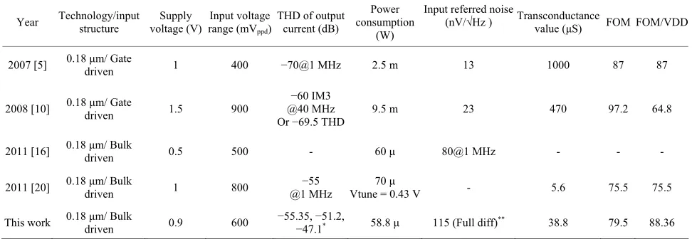
−40˚C to 70˚C. As can be seen in these tables, the OTA shows proper operation in process and temperature varia- tions. Performance comparison of the OTA with recently published work are presented in Table 4. For better comparison, a figure of merit (FOM) which is defined in [10] is used. In this FOM, shown in Equation (10),
Figure 4. Transconductance tuning versus differential input voltage.
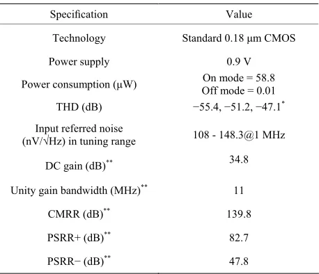
Table 1. Performance summary of the proposed OTA.
Specification Value
Technology Standard 0.18 μm CMOS
Power supply 0.9 V
Power consumption (μW) Off mode = 0.01 On mode = 58.8 THD (dB) −55.4, −51.2, −47.1* Input referred noise
(nV/√Hz) in tuning range 108 - 148.3@1 MHz
DC gain (dB)** 34.8
Unity gain bandwidth (MHz)** 11
CMRR (dB)** 139.8
PSRR+ (dB)** 82.7
PSRR− (dB)** 47.8
*At 400, 500 and 600 mV
[image:6.595.309.538.501.698.2]Table 2. Corner case simulations of the OTA.
TT SS SF FS FF Power consumption (μW) 58.8 Off = 0.001 55.9 Off = 0.0006 58.7 Off = 0.0006 58.4 Off = 0.2 60.5 Off = 0.2
THD (dB) (500 mVppd input signal)* −51.2 −48.8 −42.8 −49.8 −44.6
Input referred noise (nV/√Hz)* 115 124.6 109.2 123.5 120.9
[image:7.595.74.540.200.258.2]*@1 MHz, Vtune = 65 mV.
Table 3. Process and temperature worst case performances of the proposed OTA.
Min Typical Max
Power consumption in on mode (μW) 48.8 58.8 65.2
THD (dB) for 500 mVppd input signal* −55.7 −51.2 −40.1
Input referred noise (nV/√Hz)* 111.7 115 149.4
[image:7.595.55.541.300.468.2]*@1 MHz, Vtune = 65 mV.
Table 4. Performance summary of the OTA and comparison with recently published work.
Year Technology/input structure voltage (V) Supply range (mVInput voltage ppd)
THD of output current (dB)
Power consumption
(W)
Input referred noise
(nV/√Hz ) Transconductance value (μS) FOM FOM/VDD
2007 [5] 0.18 driven μm/ Gate 1 400 −70@1 MHz 2.5 m 13 1000 87 87
2008 [10] 0.18 driven μm/ Gate 1.5 900
−60 IM3 @40 MHz Or −69.5 THD
9.5 m 23 470 97.2 64.8
2011 [16] 0.18 driven μm/ Bulk 0.5 500 - 60 μ 80@1 MHz - - -
2011 [20] 0.18 driven μm/ Bulk 1 800 @1 MHz −55 Vtune = 0.43 V70 μ - 5.6 75.5 75.5
This work 0.18 driven μm/ Bulk 0.9 600 −55.35, −47.1−51.2, * 58.8 μ 115 (Full diff)** 38.8 79.5 88.36 *At 400, 500 and 600 mVppd input signal, respectively (@1 MHz, Vtune = 65 mV); **@1 MHz, Vtune = 65 mV.
transconductance value, linearity performance, speed of the circuit, input swing amplitude, and power consump- tion are considered.
0
10logGm Vid THD f FOM
P
(10)
We have also included a new measure, defined as FOM/VDD, in this table to account for the effect supply voltage reduction. As can be seen, by including the effect of supply voltage, it is obvious that the proposed OTA compares well with the others.
4.2. Simulation Results of the Gm-C Filter The filter is designed for cut off frequency of more than 1 MHz. This condition guarantees that the filter never removes desired signal power. This consideration is mentioned as the design should be able to compensate the transfer function distortion of the filter (i.e., reduction of the cut off frequency). This distortion comes from truning on the parallel transconductors which leads to
reducing output impedance of the related stage.
Figure 5 shows the frequency response of the third order Butterworth low-pass filter over gain tuning of the filter. This filter has gain tuning from 5 dB to 21 dB with 4 dB gain steps. As can be seen in this figure, the cut off frequency of the filter is more than 1 MHz in complete range of the gain tuning. The proposed filter achieves attenuation of 32.1 dB and 50.2 dB at 5 MHz and 10 MHz, respectively for a 5 dB gain of the filter. The pro- posed filter consumes 411.6 μW to 646.8 μW powers for 5 dB to 21 dB gains of the filter.
The input referred noise of the filter is simulated as 67 nV/√Hz at maximum gain of the filter, which is in- creased to 167.1 nV/√Hz at minimum gain. This noise value seems good for bulk driven filter with low supply voltage. The simulated in-band IIP3 of the filter is shown
in Figure 6 which is 10.75 dBm at a 5 dB gain. This IIP3
value is measured with two input tones of 0.99 MHz and 1.01 MHz. The simulations show that the IIP3 is reduced
-8 -6 -4 -2 0 2 4 6 8
-10 10
-35 -25 -15 -5 5 15
-45 25
H
Ma
gn
it
ud
e (
dB)
Frequency (MHz)
(a)
-1.5 -1.0 -0.5 0.0 0.5 1.0 1.5
-2.0 2.0
0 5 10 15 20
-5 25
H
Ma
gn
it
ud
e (
dB)
[image:8.595.70.278.82.488.2]Frequency (MHz) (b)
Figure 5. Frequency response of the third order low-pass filter. (a) Total response; (b) Zoom in on the pass band of the frequency response
-35 -30 -25 -20 -15 -10 -5 0 5 10
-40 15
-120 -100 -80 -60 -40 -20 0
-140 20
Po
ut
(
dBm
)
[image:8.595.309.537.391.574.2]Pin (dBm) Fundamental In-band IM3
Figure 6. In-band IIP3 calculation for a 5 dB gain of the filter.
The simulated performances of the filter are listed in Table 5. Corner case simulations of the filter are pre- sented in Table 6. Corner cases and temperature varia- tions from −40˚C to 70˚C are simulated as well, and show IIP3 better than 7 dBm, cut off frequency better
than 1.2 MHz, attenuation at 5 MHz better than 31 dB and attenuation at 10 MHz better than 49.2 dB, in worst cases, for 5 dB gain of the filter. These values show that the filter operates properly in process and temperature variations. In order to compensate corner case and tem- perature variations, the Vtune of the tuning transistor is adjusted to obtain appropriate gain of filter and cut off frequency more than 1 MHz. The performance compare- son of the filter with recently published work is included in Table 7. Performances of the proposed filter are cal- culated at 5 dB gain of the filter. For better comparison, a figure of merit (FOM) is used as follows [24]:
2 3 3 4 3,
C
N c
P
IIP N
FOM SFDR
P f SFDRN
(11)
in which, Pcis the power consumption of the filter, N is the number of poles and zeros, fc is the cutoff frequency
Table 5. Performance summary of the proposed filter.
Specification Value
Technology 0.18 μm CMOS
Power supply 0.9 V
Filter type 3rd order low-pass Butterworth
Cut off frequency (MHz) More than 1
Gain tuning (dB) 5 to 21
Attenuation (dB) 32.1@5 MHz
*
50.2@10 MHz*
Power consumption (μW) 411.6, 646.8** Differential output swing (V) 0.86*
IIP3 (dBm) 10.75, −7** Input referred noise @1 MHz
(nV/√ Hz) 67, 167.1**
*At 5 dB gain of the filter; **At 5 dB and 21 dB gain of filter, respectively.
Table 6. Corner case simulation results of the filter (Vtune is adjusted per corner case to obtain gain = 5 dB and fc > 1 MHz).
Performances at 5 dB gain of the
filter TT SS SF FS FF
IIP3 (dBm) 10.75 9.5 11.5 11 11.5
Noise figure (dB) 45.2 46 45.7 45.8 45.26
Cut off frequency (MHz) 1.4 1.3 1.3 1.3 1.3
Attenuation (dB) @5 MHz 32.1 34.3 32.7 34.4 32.7
[image:8.595.78.272.542.709.2] [image:8.595.310.539.633.736.2]Table 7. Performance summary of the filter and comparison with recently published work.
FOM* VDD FOM
(fJ) Cut off frequency
(MHz) Order of
low-pass filter Input referred noise
(nV/√Hz) IIP3 (dBm)
Power consumption (W) VDD (V)
Technology/ input structure Year
0.02* 0.02* 8.1 - 13.5
6 (Diff) 75
21.7 - 22.1 4.35 m
1 90 nm/gate
driven 2011 [24]
1.85* 1.54* 0.5 - 20
3 12 - 425
19 - 22.3 4.1 m - 11.1 m
1.2 0.18 μm/gate
driven 2009 [25]
- - 1.4 - 6
3 171 (@1 MHz)
- 326 μ
0.5 0.18 μm/bulk
driven 2011 [16]
0.37** 0.41** 1
3 (Diff) 167.1@1 MHz** 10.75**
411.6 μ** 0.9
0.18 μm/bulk driven This work
*Average of FOM, **@5 dB gain.
and the SFDR.N4/3 expression is the normalized spurious
free dynamic range [24]. For a better comparison of the designs, the average of the FOM is used for filters with cut off frequency tuning. In contrast with the FOM de- fined for the OTA in Equation (10), the lower FOM in Equation (11) shows a better design. Therefore, for tak- ing effects of supply voltage into account, FOM*VDD is
included also in Table 7. This table shows that the pro- posed filter compares favorably with others.
5. Discussion/Analysis
In this paper, a 0.9 V supply transconductance with bulk driven input pairs is represented. A range of 40% tuning of the transconductance value is achieved by varying the source degeneration resistance, which is also used for further improving linearity. This tuning can be used for compensating PVT variations and achieving gain tuning for a third order Butterworth low-pass filter. Further gain tuning of the filter is achieved by parallelizing of trans- conductor blocks. Using these two methods the gain of the filter can be tuned from 5 dB to 21 dB.
The OTA and filter are simulated in a standard 0.18
μm CMOS technology. The OTA consumes 58.8 μW and filter consumes 411.6 μW to 646.8 μW powers for 5 dB to 21 dB gains. The OTA shows input reffered noise of 108 nV/√Hz to 148.3 nV/√Hz over tuning range of the transconductance value, which is due to the resistance variation of the tuning transistor. The filter shows 167.1 nV/√Hz input reffered noise and 10.75 dBm IIP3 at 5 dB gain, too. Process corners and temperature variations from −40˚C to 70˚C are also studied in the paper to fore- cast the operation of the OTA and filter after fabrication. The simulations show good stability in all process cor- ners and temperatures.
6. Conclusions
A low supply transconductance with bulk driven input pair is proposed in this work. Linearity improvement of the OTA is done by attenuation and source degeneration techniques. Attenuation is implemented by a bulk driven
cell, which is used to overcome the threshold voltage limitations of the transistor in low supply voltage circuits. A transconductance enhancement technique is applied to the input pairs of the transconductor to ovecome some drawbacks of the bulk diven cell, including low trans- conductance value, low DC gain, and high noise. The high noise drawback of the bulk driven cell could be fur- ther reduced by some noise cancellation technique. A self cascode structure is also applied to the output stage of the transconductor for further enhancing the DC gain.
As an application of the proposed low voltage OTA, a third order low-pass filter is implemented. The gain of the filter can be tuned. This tunable filter can be used as a channel select filter and variable gain amplifier for wire- less sensor network (WSN) applications. The simulation results prove that the proposed design satisfies the re- quired performance of the ZigBee standard, used for wireless sensor network applications.
REFERENCES
[1] A. El Mourabit, G. Lu and P. Pittet, “Wide-Linear-Range Subthreshold OTA for Low-Power, Low-Voltage, and Low-Frequency Applications,” IEEE Transactions on Circuits and Systems I, Vol. 52, No. 8, 2005, pp. 1481- 1488. doi:10.1109/TCSI.2005.852011
[2] A. Worapishet and C. Naphaphan, “Current-Feedback Source-Degenerated CMOS Transconductor with Very High Linearity,” Electronics Letters, Vol. 39, No. 7, 2003, pp. 17-18. doi:10.1049/el:20030050
[3] A. J. López-Martín, J. Ramirez-Angulo, C. Durbha and R. G. Carvajal, “A CMOS Transconductor with Multidecade Tuning Using Balanced Current Scaling in Moderate In-version,” IEEE Journal of Solid-State Circuits, Vol. 40, No. 5, 2005, pp. doi:10.1109/JSSC.2005.845980
[4] F. A. P. Barúqui and A. Petraglia, “Linearly Tunable CMOS OTA with Constant Dynamic Range Using Source-Degenerated Current Mirrors,” IEEE Transac-tions on Circuits and Systems II, Vol. 53, No. 9, 2006, pp. 791-801. doi:10.1109/TCSII.2006.881162
54, No. 12, 2007, pp. 1047-1051. doi:10.1109/TCSII.2007.907559
[6] K. Kwon, H.-T. Kim and K. Lee, “A 50 - 300-MHz Highly Linear and Low-Noise CMOS Gm-C Filter Adopting Multiple Gated Transistors for Digital TV Tuner ICs,” IEEE Transactions on Microwave Theory and Techniques, Vol. 57, No. 2, 2009, pp. 306-313. doi:10.1109/TMTT.2008.2009904
[7] H. Le-Thai, H.-H. Nguyen, H.-N. Nguyen, H.-S. Cho, J.-S. Lee, et al., “An IF Bandpass Filter Based on a Low Distortion Transconductor,” IEEE Journal of Solid-State Circuits, Vol. 45, No. 11, 2010, pp. 2250-2261.
doi:10.1109/JSSC.2010.2063991
[8] A. Lewinski and J. S. Martinez, “OTA Linearity En-hancement Technique for High Frequency Applications With IM3 Below −65 dB,” IEEE Transactions on Cir-cuits and Systems II, Vol. 51, No. 10, 2004, pp. 542-548. doi:10.1109/TCSII.2004.834531
[9] S. Ouzounov, E. Roza, J. A. (Hans) Hegt, G. Weide and A. H. M. van Roermund, “A CMOS V-I Converter with 75-dB SFDR and 360-μW Power Consumption,” IEEE Journal of Solid-State Circuits, Vol. 40, No. 7, 2005, pp. 1527-1532. doi:10.1109/JSSC.2005.847496
[10] T.-Y. Lo and C.-C. Hung, “A 40-MHz Double Differen-tial-Pair CMOS OTA with −60-dB IM3,” IEEE Transac-tions on Circuits and Systems I, Vol. 55, No. 1, 2008, pp. 258-265. doi:10.1109/TCSI.2007.910747
[11] C. I. Luján-Martinez, R. G. Carvajal, A. Torralba, A. J. Lopez-Martin, J. Ramirez-Angulo, et al., “Low-Power Baseband Filter for Zero-Intermediate Frequency Digital Video Broadcasting Terrestrial/Handheld Receivers,” IET Circuits, Devices and Systems, Vol. 3, No. 5, 2009, pp. 291-301. doi:10.1049/iet-cds.2008.0326
[12] U. Yodprasit and C. C. Enz, “A 1.5-V 75-dB Dynamic Range Third-Order Gm-C Filter Integrated in a 0.18-μm Standard Digital CMOS Process,” IEEE Journal of Solid- State Circuits, Vol. 38, No. 7, 2003, pp. 1189-1197. doi:10.1109/JSSC.2003.813293
[13] S. Han, “A Novel Tunable Transconductance Amplifier Based on Voltage-Controlled Resistance by MOS Tran-sistors,” IEEE Transactions on Circuits and Systems II, Vol. 53, No. 8, 2006, pp. 662-666.
doi:10.1109/TCSII.2006.875309
[14] E. Sánchez-Sinencio and J. Silva-Martinez, “CMOS Transconductance Amplifiers, Architectures and Active Filters: A Tutorial,” IEEE Proceedings Circuits, Devices and Systems, Vol. 147, No. 1, 2000, pp. 3-12.
doi:10.1049/ip-cds:20000055
[15] J. M. Carrillo ,G. Torelli, R. P. Aloe, J. M. Valverde and J. F. Duque-Carrillo, “Single-Pair Bulk-Driven CMOS In-put Stage: A Compact Low-Voltage Analog Cell for
Scaled Technologies,” Integration, the VLSI journal, Vol. 43, No. 3, 2010, pp. 251-257.
doi:10.1016/j.vlsi.2010.03.002
[16] F. Rezaei and S. J. Azhari, “Ultra Low Voltage, High Performance Operational Transconductance Amplifier and Its Application in A Tunable Gm-C Filter,” Microe-lectronics Journal, Vol. 42, No. 6, 2011, pp. 827-836. doi:10.1016/j.mejo.2011.04.012
[17] J. M. Carrillo, G. Torelli and J. F. Duque-Carrillo, “Transconductance Enhancement in Bulk-Driven Input Stages and Its Applications,” Analog Integrated Circuits and Signal Processing, Vol. 68, No. 2, 2011, pp. 207-217. doi:10.1007/s10470-011-9603-z
[18] R. G. Carvajal, J. R. Angulo, A. J. López-Martín, A. Tor-ralba, J. Antonio Gómez Galán, et al., “The Flipped Voltage Follower: A Useful Cell for Low-Voltage Low- Power Circuit Design,” IEEE Transactions on Circuits and Systems I, Vol. 52, No. 7, 2005, pp. 1276-1291. doi:10.1109/TCSI.2005.851387
[19] T.-Y. Lo and C.-C. Hung, “A 250 MHz Low Voltage Low-Pass Gm-C Filter,” Analog Integrated Circuits and Signal Processing, Vol. 71, No. 3, 2012, pp. 465-472. doi:10.1007/s10470-011-9666-x
[20] Y. H. Kong, H. Yang, M. Jiang, S. Z. Xu and H. Z. Yang, “Low-Voltage Transconductor with Wide Input Range and Large Tuning Capability,” Tsinghua Science and Technology, Vol. 16, No. 1, 2011, pp. 106-112.
doi:10.1016/S1007-0214(11)70017-7
[21] S. S. Rajput and S. S. Jamuar, “Low Voltage Analog Circuit Design Techniques,” IEEE Circuits and Systems Magazine, Vol. 2, No. 1, 2002, pp. 24-42.
doi:10.1109/MCAS.2002.999703
[22] N.-J. Oh and S.-G. Lee, “Building a 2.4-GHz Radio Transceiver Using IEEE 802.15.4,” IEEE Circuits & De- vices Magazine, Vol. 21, No. 6, 2005, pp. 43-51. doi:10.1109/MCD.2005.1578587
[23] A. Tajalli and Y. Leblebici, “Linearity Improvement in Biquadratic Transconductor-C Filters,” Electronics Let-ters, Vol. 43, No. 24, 2007, pp. 1360-1362.
doi:10.1049/el:20072537
[24] M. S. Oskooei, N. Masoumi, M. Kamarei and H. Sjöland, “A CMOS 4.35-mW + 22-dBm IIP3 Continuously
Tun-able Channel Select Filter for WLAN/WiMAX Receiv-ers,” IEEE Journal of Solid-State Circuits, Vol. 46, No. 6, 2011, pp. 1382-1391. doi:10.1109/JSSC.2011.2120670 [25] T.-Y. Lo, C.-C. Hung and M. Ismail, “A Wide Tuning
Range Gm-C Filter for Multi-Mode CMOS Direct-Con- version Wireless Receivers,” IEEE Journal of Solid-State Circuits, Vol. 44, No. 9, 2009, pp. 2515-2524.