ADS1201
®
©1997 Burr-Brown Corporation PDS-1417C Printed in U.S.A. October, 1999
International Airport Industrial Park • Mailing Address: PO Box 11400, Tucson, AZ 85734 • Street Address: 6730 S. Tucson Blvd., Tucson, AZ 85706 • Tel: (520) 746-1111 Twx: 910-952-1111 • Internet: http://www.burr-brown.com/ • Cable: BBRCORP • Telex: 066-6491 • FAX: (520) 889-1510 • Immediate Product Info: (800) 548-6132
High Dynamic Range
DELTA-SIGMA MODULATOR
ADS1201 +2.5V Reference Bias Generator Second-Order ∆Σ ModulatorAVDD AGND REF IN REF OUT VBIAS
CAL GAIN/OFFSET DVDD DGND AINP AINN MOUT BIASEN REFEN MCLK
DESCRIPTION
The ADS1201 is a precision, 130dB dynamic range,
delta-sigma (∆Σ) modulator operating from a single
+5V supply. The differential inputs are ideal for direct connection to transducers or low level signals. With the appropriate digital filter and modulator rate, the device can be used to achieve 24-bit analog-to-digital (A/D) conversion with no missing codes. Effective resolution of 20 bits can be maintained with a digital filter bandwidth of 1kHz at a modulator rate of 320kHz. The ADS1201 is designed for use in high resolution measurement applications including smart transmit-ters, industrial process control, weigh scales, chroma-tography, and portable instrumentation. It is available in a 16-lead SOIC package.
FEATURES
● 130dB DYNAMIC RANGE
● FULLY DIFFERENTIAL INPUT
● TWO-WIRE INTERFACE
● INTERNAL/EXTERNAL REFERENCE
● ON-CHIP SWITCHES FOR CALIBRATION
APPLICATIONS
● INDUSTRIAL PROCESS CONTROL
● INSTRUMENTATION
● SMART TRANSMITTERS
● PORTABLE INSTRUMENTS
● WEIGH SCALES
At TA = +25°C, AVDD = DVDD = +5V, MCLK = 320kHz, REFEN LOW, BIASEN LOW, and external +2.5V reference, unless otherwise specified.
The information provided herein is believed to be reliable; however, BURR-BROWN assumes no responsibility for inaccuracies or omissions. BURR-BROWN assumes no responsibility for the use of this information, and all use of such information shall be entirely at the user’s own risk. Prices and specifications are subject to change without notice. No patent rights or licenses to any of the circuits described herein are implied or granted to any third party. BURR-BROWN does not authorize or warrant any BURR-BROWN product for use in life support devices and/or systems.
SPECIFICATIONS
ADS1201U
PARAMETER CONDITIONS MIN TYP MAX UNITS ANALOG INPUT
Absolute Input Voltage Range 0 +5 V
With VBIAS(1) –10 +10 V
Differential Input Voltage Range –5 +5 V
With VBIAS(1) –20 See Note 2 +20 V
Input Impedance 250(4) kΩ
Input Capacitance 8 pF
Input Leakage Current 5 50 pA
At TMIN to TMAX 1 nA
SYSTEM PERFORMANCE
Dynamic Range 10Hz Bandwidth(5) 130(6) dB
60Hz Bandwidth(5) 115(6) 120(6) dB
1kHz Bandwidth(5) 115(6) dB
Integral Linearity Error 60Hz Bandwidth(5) ±0.0015 %FSR
1kHz Bandwidth(5) ±0.0015 %FSR
Offset Error(2) See Note 7 µV
Offset Drift(3) 1 µV/°C
Gain Error(2) See Note 7 ppm
Gain Error Drift(3) 1 µV/°C
Common-Mode Rejection At DC 80 100 dB
Power Supply Rejection 80 dB
REFERENCE
Internal Reference (REFOUT) 2.4 2.5 2.6 V
Drift 25 ppm/°C
Noise 50 µVp-p
Load Current Source or Sink –1 1 mA
Output Impedance 2 Ω
External Reference (REFIN) 2.0 3.0 V
Load Current 2.5 µA
VBIAS Output Using Internal Reference 3.15 3.3 3.45 V
Drift 50 ppm/°C
Load Current 10 mA
DIGITAL INPUT/OUTPUT
Logic Family TTL Compatible CMOS
Logic Levels: VIH (MCLK) IIH = +5µA 2.0 DVDD +0.3 V VIL (MCLK) IIL = +5µA –0.3 0.8 V VOH (MOUT) IOH = 2 TTL Loads 2.4 V VOL (MOUT) IOL = 2 TTL Loads 0.4 V MCLK Frequency 0.02 1 MHz
POWER SUPPLY REQUIREMENTS
Power Supply Voltage Specified Performance 4.75 5.25 V
Supply Current
Analog Current 4.6 mA
Digital Current 0.4 mA
Additional Analog Current
REFOUT Enabled No Load 1.6 mA
VBIAS Enabled No Load 1 mA
Total Power Dissipation REFOUT, VBIAS Disabled 25 40 mW
TEMPERATURE RANGE
Specified Performance –40 +85 °C
NOTES: (1) This range is set with external resistors and VBIAS (as described in the text). Other ranges are possible. (2) After the on-chip offset and gain calibration functions have been employed. (3) Re-calibration can reduce these errors. (4) Input impedance changes with MCLK. (5) Assume brick wall digital filter is used. (6) 20 Log (full scale/r ms noise). (7) After calibration, these errors will be of the order of the effective resolution.
®
Analog Input: Current ...±100mA, Momentary
±10mA, Continuous Voltage ... AGND –0.3V to AVDD +0.3V AVDD to DVDD... –0.3V to 6V AVDD to AGND ... –0.3V to 6V DVDD to DGND ... –0.3V to 6V AGND to DGND ...±0.3V REFIN Voltage to AGND ... –0.3V to AVDD +0.3V Digital Input Voltage to DGND ... –0.3V to DVDD +0.3V Digital Output Voltage to DGND ... –0.3V to DVDD +0.3V Lead Temperature (soldering, 10s) ... +300°C Internal Power Dissipation ... 500mW
NOTE: (1) Stresses above those listed under “Absolute Maximum Ratings” may cause permanent damage to the device. Exposure to absolute maximum conditions for extended periods may affect device reliability.
ABSOLUTE MAXIMUM RATINGS
ELECTROSTATIC
DISCHARGE SENSITIVITY
This integrated circuit can be damaged by ESD. Burr-Brown recommends that all integrated circuits be handled with appropriate precautions. Failure to observe proper handling and installation procedures can cause damage.
ESD damage can range from subtle performance degradation to complete device failure. Precision integrated circuits may be more susceptible to damage because very small parametric changes could cause the device not to meet its published specifications.
PACKAGE SPECIFIED
DRAWING TEMPERATURE PACKAGE ORDERING TRANSPORT PRODUCT PACKAGE NUMBER RANGE MARKING NUMBER(1) MEDIA
ADS1201U SOL-16 211 –40°C to +85°C ADS1201U ADS1201U Rails
" " " " " ADS1201U/1K Tape and Reel
NOTE: (1) Models with a slash (/) are available only in Tape and Reel in the quantities indicated (e.g., /1K indicates 1000 devices per reel). Ordering 1000 pieces of “ADS1201U/1K” will get a single 1000-piece Tape and Reel.
PACKAGE/ORDERING INFORMATION PIN CONFIGURATION
Top View SOIC
1 AVDD Analog Input: Analog Supply, +5V nominal. 2 REFOUT Analog Output: Internal Reference Voltage Output:
+2.5V nominal.
3 REFIN Analog Input: Reference Voltage Input. 4 NIC Not Internally Connected.
5 AINP Analog Input: Noninverting Input. 6 AINN Analog Input: Inverting Input. 7 AGND Analog Input: Analog Ground.
8 VBIAS Analog Output: Bias Voltage Output, nominally +3.3V (with +2.5V reference).
9 BIASEN Digital Input: Bias Voltage Enable Input (HIGH = enabled, LOW = disabled).
10 GAIN/OFFSET Digital Input: Gain/Offset Calibration Select Input (with CAL LOW; HIGH = gain configuration, LOW = offset configuration).
11 CAL Digital Input: Calibration Control Input (HIGH = normal operation, LOW = gain or offset calibration configuration).
12 DGND Digital Input: Digital Ground.
13 DVDD Digital Input: Digital Supply, +5V nominal. 14 MCLK Digital Input: Modulator Clock Input. CMOS
compatible.
15 MOUT Digital Output: Modulator Output. 16 REFEN Digital Input: REFOUT Voltage Enable Input
(HIGH = enabled, LOW = disabled). PIN DESCRIPTIONS
PIN NO NAME DESCRIPTION
ADS1201 1 2 3 4 5 6 7 8 16 15 14 13 12 11 10 9 AVDD REFOUT REFIN NIC AINP AINN AGND VBIAS REFEN MOUT MCLK DVDD DGND CAL GAIN/OFFSET BIASEN
TYPICAL PERFORMANCE CURVES
At TA = +25°C, AVDD = DVDD = +5V, MCLK = 320kHz, REFEN LOW, BIASEN LOW, and external +2.5V reference, unless otherwise specified.
1.2 1 0.8 0.6 0.4 0.2 0 rms NOISE VDIN (V) –5 –4 –3 –2 –1 0 1 2 3 4 5 (ppm) 1.5 1.0 0.5 0 –0.5 –1.0 –1.5 –2.0 –2.5 –3.0 –3.5 LINEARITY VDIN (V) –5 –4 –3 –2 –1 0 1 2 3 4 5 (ppm) 110 105 100 95 CMRR vs FREQUENCY Frequency (Hz) 0.1 1 10 100 1000 CMRR (dB) 70 68 66 64 62 60 PSRR vs FREQUENCY Frequency (Hz) 0.1 1.0 10 100 1k 10k 100k PSRR (dB) 30 25 20 15 10 5 0
TYPICAL SINK CURRENT
VOL (V) 0 0.5 1.0 1.5 2.0 2.5 3.0 3.5 4.0 4.5 5.0 IOUT (mA) 30 25 20 15 10 5 0
TYPICAL SOURCE CURRENT
VOL (V)
0 0.5 1.0 1.5 2.0 2.5 3.0 3.5 4.0 4.5 5.0
IOUT
®
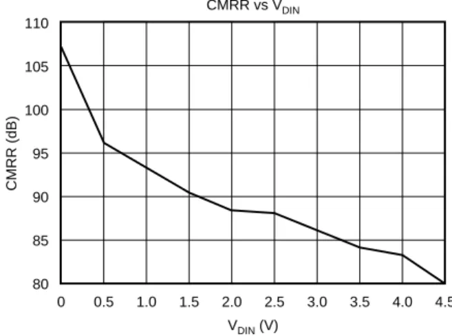
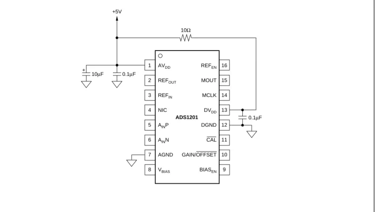
FIGURE 1. Connection Diagram for the ADS1201 Delta-Sigma Modulator Including External Processor. 110 105 100 95 90 85 80 CMRR vs VDIN VDIN (V) 0 0.5 1.0 1.5 2.0 2.5 3.0 3.5 4.0 4.5 CMRR (dB)
TYPICAL PERFORMANCE CURVES
(Cont.)
At TA = +25°C, AVDD = DVDD = +5V, MCLK = 320kHz, REFEN LOW, BIASEN LOW, and external +2.5V reference, unless otherwise specified.
ADS1201 1 2 3 4 5 6 7 8 16 15 14 13 12 11 10 9 AVDD REFOUT REFIN NIC AINP AINN AGND VBIAS REFEN MOUT MCLK DVDD DGND CAL GAIN/OFFSET BIASEN Processor 200Ω Analog Supply 10µF 0.1µF Digital Supply 200Ω 0.1µF 47pF 47pF
GENERAL DESCRIPTION
The ADS1201 is a single channel, second-order, CMOS analog modulator designed for high resolution conversions from dc to 1000Hz. The output of the converter (MOUT) provides a stream of digital ones and zeros. The time average of this serial output is proportional to the analog input voltage. The combination of an ADS1201 and a processor that is programmed to implement a digital filter results in a high resolution A/D converter system. This system allows flexibility with the digital filter design and is capable of A/D conversion results that have a dynamic range that exceeds 130dB (see Figure 1).
THEORY OF OPERATION
The differential analog input of the ADS1201 is imple-mented with a switched capacitor circuit. This switched capacitor circuit implements a 2nd-order modulator stage which digitizes the input signal into a binary output stream. The input stage of the converter can be configured to sample an analog signal or to perform a calibration which quantifies offset and gain errors. The sample clock (MCLK) provides the switched capacitor network and modulator clock signal for the A/D conversion process, as well as the output data framing clock. Different frequencies for this clock allows for a variety of performance solutions in resolution and signal bandwidth. The analog input signal is continuously sampled by the A/D converter and compared to an internal or external voltage reference. A digital stream appears at the output of the converter. This digital stream accurately repre-sents the analog input voltage over time.
FIGURE 2. Block Diagram of the ADS1201.
FIGURE 3. Input Impedance of the ADS1201.
out of the analog inputs exceed 10mA. In addition, the linearity of the device is guaranteed only when the analog voltage applied to either input resides within the range
defined by AGND = > –30mV and < = AVDD + 30mV. If
either of the inputs exceed these limits, the input protection diodes on the front end of the converter will begin to turn on. This will induce leakage paths resulting in nonlinearities in the conversion process.
For this reason, the 0V to 5V input range must be used with
caution. Should AVDD be 4.75V, the analog input signal
would swing outside the guaranteed specifications of the device. Designs utilizing this mode of operation should consider limiting the span to a slightly smaller range. Com-mon-mode voltages are also a significant concern and must be carefully analyzed.
Modulator
The modulator sampling frequency (MCLK) can be oper-ated over a range of 20kHz to 1MHz. The frequency of MCLK can be increased to improve the performance of the converter or adjusted to comply with the clock requirements of the application.
The modulator topology is fundamentally a 2nd-order, charge-balancing A/D converter, as the one conceptualized in Fig-ure 4. The analog input voltage and the output of the 1-bit
DAC is differentiated, providing an analog voltage at X2 and
X3. The voltage at X2 and X3 are presented to their
indi-vidual integrators. The output of these integrators progress in a negative or positive direction. When the value of the
signal at X4 equals the comparator reference voltage, the
output of the comparator switches from negative to positive or positive to negative, depending on its original state. When the output value of the comparator switches from a HIGH to LOW or vise versa, the 1-bit DAC responds on the next
clock pulse by changing its analog output voltage at X6,
causing the integrators to progress in the opposite direction. The feedback of the modulator to the front end of the integrators force the value of the integrator output to track the average of the input.
ANALOG INPUT STAGE
Analog Input
The input design topology of the ADS1201 is based on a fully differential switched capacitor architecture. This input stage provides the mechanism to achieve low system noise, high common-mode rejection (100dB) and excellent power supply rejection. The input impedance of the analog input is dependent on the input capacitor and modulator clock fre-quency (MCLK), which is also the sampling frefre-quency of the converter. Figure 3 shows the basic input structure of the ADS1201. The relationship between the input impedance of the ADS1201 and the modulator clock frequency is:
The input impedance becomes a consideration in designs where the source impedance of the input signal is signifi-cant. In this case, it is possible for a portion of the signal to be lost across this external source impedance. The impor-tance of this effect depends on the desired system perfor-mance.
There are two restrictions on the analog input signal to the ADS1201. Under no conditions should the current into or
1-Bit DAC Switched Capacitor Analog Input 2nd-Order Charge-Balancing A/D Converter Analog Inputs 1-Bit Data Stream Processor for Filtering
Programmable Gain Amp
VREF VIN– VIN+ 2nd-Order Modulator RSW 8kΩ (typ) Switching Frequency = MCLK High Impedance > 1GΩ CINT 12pF (typ) VCM AIN+ RSW 8kΩ (typ) High Impedance > 1GΩ CINT 12pF (typ) AIN– A Input pedance E f IN MCLK Im ( ) • Ω = 1 12 12
®
FIGURE 4. Block Diagram of a Second-Order Modulator.
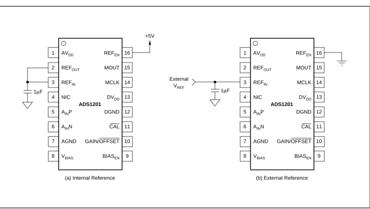
FIGURE 5. Two Voltage Reference Connection Alternatives for the ADS1201. REFERENCE CIRCUIT
There are two reference circuits included in the ADS1201 converter: VREF (REFIN, REFOUT) and VBIAS. The circuitry
for VREF is configured to allow the user to utilize the internal
reference on the chip or provide an external reference to the
converter (see Figure 5). The second reference, VBIAS, is
derived from VREF, whether it is internal or external. VBIAS
is exclusively an output reference. This ratiometric
relation-ship between VREF and VBIAS reduces system errors when
two separate bias voltages are required in the application.
REFERENCE INPUT (REFIN)
The reference input (REFIN) of the ADS1201 can be
config-ured so that the 2.5V (nominal) internal or external reference can be used in the conversion process. If the internal
refer-ence is used, the correct connection configuration is shown in Figure 5a. The capacitor in this circuit is absolutely required if low noise performance is desired.
An external reference can be used to reduce the noise in the conversion process. If an external reference is used, care should be taken to insure that the selected reference has low noise performance. The appropriate connection circuit of an external reference is shown in Figure 5b. The reference must be configured with appropriate capacitors to reduce the high frequency noise that may be contributed by the reference.
The input impedance of REFIN changes with the modulator
clock frequency. The relationship is:
ADS1201
(a) Internal Reference (b) External Reference
1 2 3 4 5 6 7 8 16 15 14 13 12 11 10 9 AVDD REFOUT REFIN NIC AINP AINN AGND VBIAS REFEN MOUT MCLK DVDD DGND CAL GAIN/OFFSET BIASEN 1µF +5V ADS1201 1 2 3 4 5 6 7 8 16 15 14 13 12 11 10 9 AVDD REFOUT REFIN NIC AINP AINN AGND VBIAS REFEN MOUT MCLK DVDD DGND CAL GAIN/OFFSET BIASEN 1µF External VREF
Typical REF Input pedance E f IN MCLK Im • = 1 12 50 VREF X4 X6 Integrator 2 Comparator fMCLK MOUT D/A Converter X3 X2 X(t) fS Integrator 1
FIGURE 7. Timing Diagram for the Digital Interface of the ADS1201.
FIGURE 6. ±10V Bipolar Input Configuration Using VBIAS.
REFEN REFOUT
LOW High Impedance
HIGH 2.5V (nominal)
TABLE I. Reference Enable.
The reference input voltage can vary between 2V and 3V. Higher reference voltages will cause the full-scale range to increase while the internal circuit noise of the converter remains approximately the same. This will increase the LSB weight but not the internal noise, resulting in increased signal-to-noise ratio. Likewise, lower reference voltages will decrease the signal-to-noise ratio.
The internal reference, which generates +2.5V, can be dis-abled when an external reference is used. This internal
reference is disabled with the REFEN pin. When the
refer-ence is disabled, the supply current (AVDD) of the converter
will reduce by approximately 1.6mA. REFERENCE OUTPUT (VREFOUT)
The ADS1201 contains an internal +2.5V reference. When
using this feature, REFEN must be HIGH (see Figure 5).
Tolerances, drift, noise, and other specifications for this
reference are given in the Specifications table. Note that this reference is not designed to sink or to source more than 1mA of current. In addition, loading the reference with a dynamic or variable load is not recommended. This can result in small changes in reference voltage as the load changes. VOLTAGE BIAS OUTPUT (VBIAS)
The VBIAS output voltage is dependent on the reference
input (REFIN) voltage and is approximately 1.33 times as
great. The output of VBIAS is used to bias input signals of
greater than 5V. If a resistor network is used in combination
with the VBIAS output, the signal range can be scaled and
level shifted to match the input range of the ADS1201. Figure 6 shows a connection diagram which will allow the
ADS1201 to accept a ±10V input signal (20V full-scale
range). If BIASEN is HIGH, the voltage at VBIAS will be
3.3V (assumes a 2.5V nominal VREF).
t4
t5
t6
Data Valid Data Valid Data Valid Data Valid t2 t1 t3 MCLK MOUT SYMBOL t1 t2 t3 t4 t5 t6 Clock Period Clock HIGH Clock LOW Clock Rise Time
Clock Fall Time DOUT Valid after Clock Rising Edge
DESCRIPTION MIN TYP
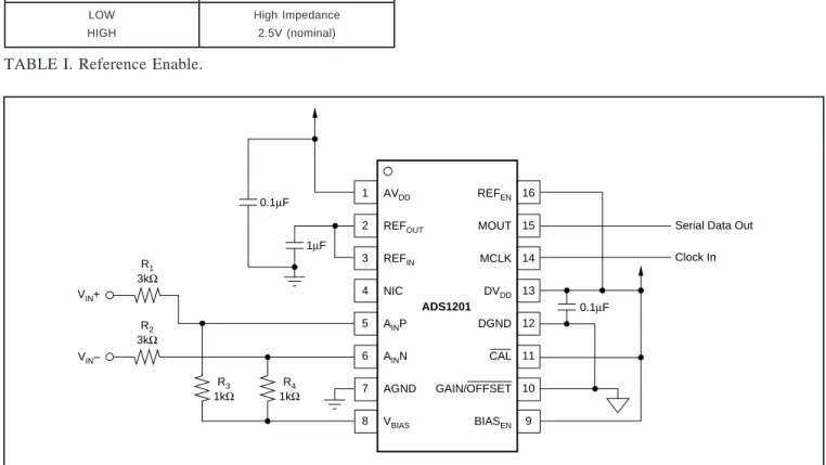
3125 1562.5 1562.5 6 6 MAX UNITS ns ns ns ns ns ns 400 ADS1201 1 2 3 4 5 6 7 8 16 15 14 13 12 11 10 9 AVDD REFOUT REFIN NIC AINP AINN AGND VBIAS REFEN MOUT MCLK DVDD DGND CAL GAIN/OFFSET BIASEN R1 3kΩ VIN+ VIN– 0.1µF 1µF
Serial Data Out Clock In R2 3kΩ 0.1µF R3 1kΩ R4 1kΩ
®
BIASEN VBIAS
LOW High Impedance
HIGH 1.33V • VREF
TABLE II. Bias Enable.
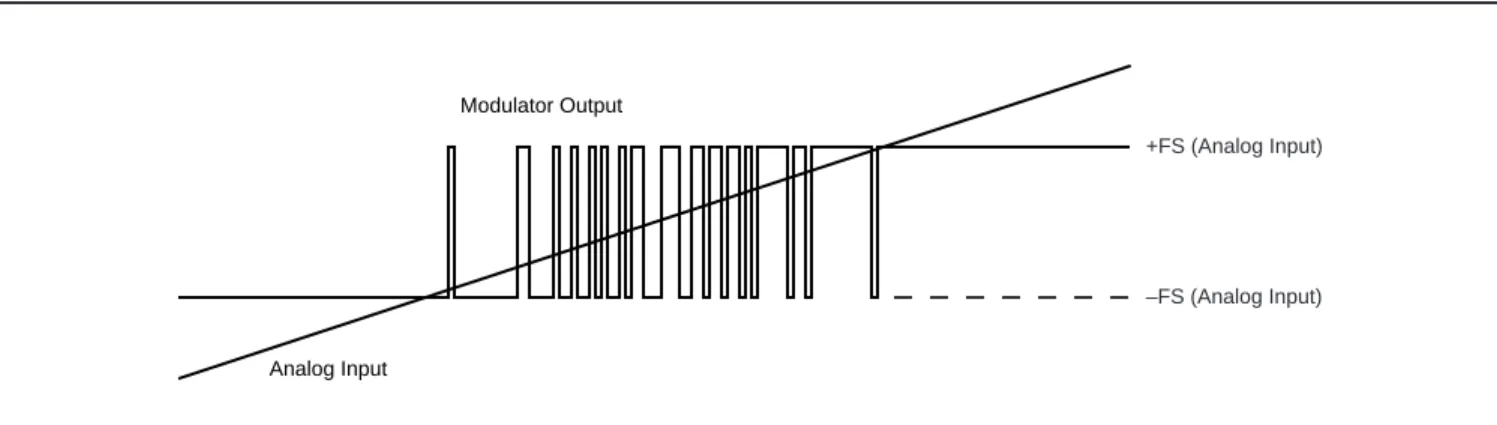
FIGURE 8. Analog Input versus Modulator Output of the ADS1201.
FIGURE 9. Timing Diagram for the Calibration Feature of the ADS1201.
When enabled, the VBIAS circuitry consumes approximately
1mA with no external load. The maximum current into or
out of VBIAS should not exceed 10mA.
On power-up, external signals may be present before VBIAS
is enabled. This can create a situation in which a negative voltage is applied to the analog inputs, reverse biasing the negative input protection diode of the ADS1201. This
situ-ation should not be a problem as long as the resistors R1 and
R2 limit the current being sourced by each analog input to be
under 10mA. A potential of 0V at the analog input pin (AINP
or AINN) should be used in the calculation.
DIGITAL OUTPUT
The timing diagram for the ADS1201 data retrieval is shown in Figure 7. MCLK initiates the modulator process for the ADS1201 and is used as a system clock by the ADS1201, as well as a framing clock for data out. The modulator output data, which is a serial stream, is available on the MOUT pin. Typically, MOUT is read on the falling edge of MCLK. Under any situation with MCLK, the duty cycle must be kept constant for reliable, repeatable results.
An input differential signal of 0V will ideally produce a stream of ones and zeros that are HIGH 50% of the time and LOW 50% of the time. A differential input of 5V will produce a stream of ones and zeros that are HIGH 90% of the time. A differential input of –5V will produce a stream of ones and zeros that are HIGH 10% of the time. The input voltage versus the output modulator signal is shown in Figure 8.
OFFSET and GAIN CALIBRATION
The ADS1201 offers a self-calibration function that is
imple-mented with the GAIN/OFFSET and CALEN pins. Both
conditions provide an output stream of data, similar to normal operation where the converter is configured to sample an input signal at AIN.
The offset and gain errors of the ADS1201 are calibrated independently. For best operation, the offset should be calibrated first, followed by the gain. The calibration imple-mentation timing diagram is shown in Figure 9. The calibra-tion mode pins control the calibracalibra-tion funccalibra-tions of the ADS1201.
Calibration should be performed once and then normal operation can be resumed. Calibration of offset and gain is recommended immediately after power-on and whenever there is a “significant” change in the operating environment. Significant changes in the operating environment include a change of the MCLK frequency, MCLK duty cycle, power
t8 t9 t11 t10 GAIN/OFFSET CAL t8 t9 SYMBOL t8 t9 t10 t11
CAL and GAIN/OFFSET Rise Time CAL and GAIN/OFFSET Fall Time GAIN/OFFSET to CAL Setup Time GAIN/OFFSET to CAL Hold Time
DESCRIPTION MIN 0 2.5 TMCLK(1) TYP 10 10 MAX UNITS ns ns ns ns NOTE: (1) TMCLK is the clock period of MCLK.
Modulator Output
Analog Input
+FS (Analog Input)
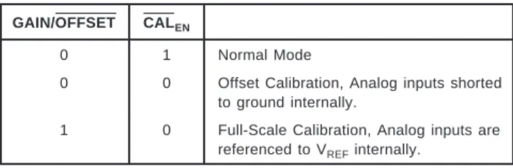
GAIN/OFFSET CALEN
0 1 Normal Mode
0 0 Offset Calibration, Analog inputs shorted to ground internally.
1 0 Full-Scale Calibration, Analog inputs are referenced to VREF internally.
TABLE III. Calibration Enable.
supply, VREF, or temperature. The amount of change which
could cause a re-calibration is dependent on the application and effective resolution of the system.
The results of the calibration calculations are stored in two registers in the processor chip (see Figure 1). These two calibration results can then be used to calibrate the input signal results with one of the following formulas:
Equivalent Calibrated Output Code = FSC (FO1 – FO2) /(FO3 – FO2) where FO1 = Filter output code of an applied input voltage
FO2 = Filter output code of the offset calibration FO3 = Filter output code of the gain calibration
FSC = Desired full-scale output
With a simple sinc filter, the calibrated A/D conversion would equal:
Equivalent Calibrated Input Voltage = (N1 – N2) • VREF/ (N3 – N2) where N1 = number of ones counted (or digital equivalent
after filtering) over given time (tM) with an applied input voltage N2 = number of ones counted (or digital equivalent after filtering) during offset calibration where t12 = tM
N3 = number of ones counted (or digital equivalent after filtering) during gain calibration where t13 = tM
A system calibration can be performed by applying two known voltage levels to the input of the converter. In this
situation, the GAIN/OFFSET and CALEN pins are not used.
Rather, the digital output of these two known voltages are accumulated by the processor. With this data, the processor can determine the calibration register values that are appro-priate for the application.
LAYOUT CONSIDERATIONS
POWER SUPPLIESThe ADS1201 requires the digital supply (DVDD) to be no
greater than the analog supply (AVDD). Failure to observe
this condition could cause permanent damage to the ADS1201. The best scheme is to power the analog section of
the design and AVDD from one +5V line and the digital
section and DVDD from a separate +5V line (from the same
supply). If there are separate analog and digital power supplies for the ADS1201, a good design approach would be to have the analog supply come up first, followed by the digital supply. Another approach that can be used to control the analog and digital power supply differences is shown in Figure 10. In this circuit, a connection has been made
between the ADS1201 supply pins via a 10Ω resistor. The
combination of this resistor and the decoupling capacitors
provides some filtering between DVDD and AVDD.
The analog supply should be well regulated and low noise. For designs requiring very high resolution from the ADS1201, power supply rejection will be a concern. The requirements for the digital supply are not strict. However, high frequency
noise on DVDD can capacitively couple into the analog
portion of the ADS1201. This noise can originate from switching power supplies, microprocessors or digital signal processors.
For either supply, high frequency noise will generally be rejected by the external digital filter at integer multiples of MCLK. Just below and above these frequencies, noise will alias back into the pass-band of the digital filter, affecting the conversion result.
Inputs to the ADS1201, such as AIN, REFIN, and MCLK,
should not be present before the analog and digital supplies are on. Violating this condition could cause latch-up. If these signals are present before the supplies are on, series resistors should be used to limit the input current.
If one supply must be used to power the ADS1201, the
system’s analog supply should be used to power both AVDD
and DVDD. Experimentation may be the best way to
deter-mine the appropriate connection between AVDD and DVDD.
GROUNDING
The analog and digital sections of the design should be carefully and cleanly partitioned. Each section should have its own ground plane with no overlap between them. AGND should be connected to the analog ground plane as well as all other analog grounds. DGND should be connected to the digital ground plane and all digital signals referenced to this plane.
The ADS1201 pinout is such that the converter is cleanly separated into an analog and digital portion. This should allow simple layout of the analog and digital sections of the design.
For a signal converter system, AGND and DGND of the ADS1201 can be connected together. Do not join the ground planes, but connect the two with a moderate signal trace underneath the converter. For multiple converters, connect the two ground planes at one location as central to all of the converters as possible. In some cases, experimentation may be required to find the best point to connect the two planes together. Experimentation may be the best way to determine the appropriate connection between AGND and DGND. DECOUPLING
Good decoupling practices should be used for the ADS1201 and for all components in the design. All decoupling
capaci-tors, specifically the 0.1µF ceramic capacitors, should be
placed as close as possible to the pin being decoupled. A 1µF and 10µF capacitor, in parallel with the 0.1µF ceramic
capacitor, should be used to decouple AVDD to AGND. At
a minimum, a 0.1µF ceramic capacitor should be used to
decouple DVDD to DGND, as well as for the digital supply
®
FIGURE 10. Power Supply Connection Using One Power Plane and One Digital Plane.
FIGURE 11. Bridge Transducer Interface with Current Excitation. ADS1201 1 2 3 4 5 6 7 8 16 15 14 13 12 11 10 9 AVDD REFOUT REFIN NIC AINP AINN AGND VBIAS REFEN MOUT MCLK DVDD DGND CAL GAIN/OFFSET BIASEN 10µF + 0.1µF +5V 10Ω 0.1µF ADS1201 1 2 3 4 5 6 7 8 16 15 14 13 12 11 10 9 AVDD REFOUT REFIN NIC AINP AINN AGND VBIAS REFEN MOUT MCLK DVDD DGND CAL GAIN/OFFSET BIASEN 1µF 0.1µF 0.1µF DSP Isolated Power MDATA MCLK SCLK SDATA Opto Coupler Opto Coupler +5V +5V +5V 1 2 8 7 5 3 4 100µA 100µA REF200 10kΩ 6kΩ
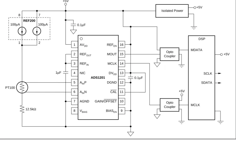
FIGURE 12. PT100 Interface with Current Excitation.
FIGURE 13. Geophone Interface.
ADS1201 1 2 3 4 5 6 7 8 16 15 14 13 12 11 10 9 AVDD REFOUT REFIN NIC AINP AINN AGND VBIAS REFEN MOUT MCLK DVDD DGND CAL GAIN/OFFSET BIASEN 1µF 0.1µF 0.1µF DSP Isolated Power MDATA MCLK SCLK SDATA Opto Coupler Opto Coupler +5V +5V +5V 1 2 8 7 100µA 100µA REF200 PT100 12.5kΩ +5V ADS1201 1 2 3 4 5 6 7 8 16 15 14 13 12 11 10 9 AVDD REFOUT REFIN NIC AINP AINN AGND VBIAS REFEN MOUT MCLK DVDD DGND CAL GAIN/OFFSET BIASEN DSP 0.1µF 0.1µF +5V MDATA MCLK SCLK SDATA 0.1µF 1/2 OPA2237 3 1 7 2 RG 10kΩ 1/2 OPA2237 6 5
®
FIGURE 14. Single-Supply, High Accuracy Thermocouple Interface.
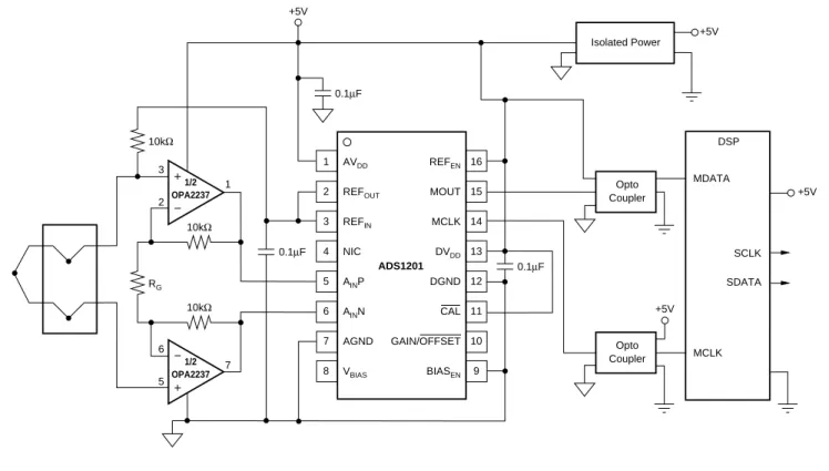
FIGURE 15. Motor Controller Sensing Circuit.
ADS1201 1 2 3 4 5 6 7 8 16 15 14 13 12 11 10 9 AVDD REFOUT REFIN NIC AINP AINN AGND VBIAS REFEN MOUT MCLK DVDD DGND CAL GAIN/OFFSET BIASEN 0.1µF 0.1µF DSP Isolated Power MDATA MCLK SCLK SDATA Opto Coupler Opto Coupler +5V +5V +5V +5V 0.1µF 1/2 OPA2237 3 1 7 2 RG 10kΩ 10kΩ 10kΩ 1/2 OPA2237 6 5 ADS1201 1 2 3 4 5 6 7 8 16 15 14 13 12 11 10 9 AVDD REFOUT REFIN NIC AINP AINN AGND VBIAS REFEN MOUT MCLK DVDD DGND CAL GAIN/OFFSET BIASEN 0.1µF 0.1µF 5.1V DSP MDATA MCLK SCLK SDATA Opto Coupler Opto Coupler +5V +5V 0.1µF RSENSE Gate Drive RSENSE Motor Floating Positive Supply HV+ HV–
PACKAGING INFORMATION
Orderable Device Status(1) Package Type
Package Drawing
Pins Package Qty
Eco Plan(2) Lead/Ball Finish MSL Peak Temp(3)
ADS1201U ACTIVE SOIC DW 16 40 Green (RoHS &
no Sb/Br)
CU NIPDAU Level-2-260C-1 YEAR
ADS1201U/1K ACTIVE SOIC DW 16 1000 Green (RoHS &
no Sb/Br)
CU NIPDAU Level-2-260C-1 YEAR
ADS1201U/1KG4 ACTIVE SOIC DW 16 1000 Green (RoHS &
no Sb/Br)
CU NIPDAU Level-2-260C-1 YEAR
ADS1201UG4 ACTIVE SOIC DW 16 40 Green (RoHS &
no Sb/Br)
CU NIPDAU Level-2-260C-1 YEAR
(1)
The marketing status values are defined as follows:
ACTIVE: Product device recommended for new designs.
LIFEBUY: TI has announced that the device will be discontinued, and a lifetime-buy period is in effect.
NRND: Not recommended for new designs. Device is in production to support existing customers, but TI does not recommend using this part in
a new design.
PREVIEW: Device has been announced but is not in production. Samples may or may not be available. OBSOLETE: TI has discontinued the production of the device.
(2)Eco Plan - The planned eco-friendly classification: Pb-Free (RoHS), Pb-Free (RoHS Exempt), or Green (RoHS & no Sb/Br) - please check http://www.ti.com/productcontentfor the latest availability information and additional product content details.
TBD: The Pb-Free/Green conversion plan has not been defined.
Pb-Free (RoHS): TI's terms "Lead-Free" or "Pb-Free" mean semiconductor products that are compatible with the current RoHS requirements
for all 6 substances, including the requirement that lead not exceed 0.1% by weight in homogeneous materials. Where designed to be soldered at high temperatures, TI Pb-Free products are suitable for use in specified lead-free processes.
Pb-Free (RoHS Exempt): This component has a RoHS exemption for either 1) lead-based flip-chip solder bumps used between the die and
package, or 2) lead-based die adhesive used between the die and leadframe. The component is otherwise considered Pb-Free (RoHS compatible) as defined above.
Green (RoHS & no Sb/Br): TI defines "Green" to mean Pb-Free (RoHS compatible), and free of Bromine (Br) and Antimony (Sb) based flame
retardants (Br or Sb do not exceed 0.1% by weight in homogeneous material)
(3)
MSL, Peak Temp. -- The Moisture Sensitivity Level rating according to the JEDEC industry standard classifications, and peak solder temperature.
Important Information and Disclaimer:The information provided on this page represents TI's knowledge and belief as of the date that it is
provided. TI bases its knowledge and belief on information provided by third parties, and makes no representation or warranty as to the accuracy of such information. Efforts are underway to better integrate information from third parties. TI has taken and continues to take reasonable steps to provide representative and accurate information but may not have conducted destructive testing or chemical analysis on incoming materials and chemicals. TI and TI suppliers consider certain information to be proprietary, and thus CAS numbers and other limited information may not be available for release.
In no event shall TI's liability arising out of such information exceed the total purchase price of the TI part(s) at issue in this document sold by TI to Customer on an annual basis.
PACKAGE OPTION ADDENDUM
www.ti.com 7-Oct-2008
TAPE AND REEL INFORMATION
*All dimensions are nominal
Device Package Type Package Drawing Pins SPQ Reel Diameter (mm) Reel Width W1 (mm) A0 (mm) B0 (mm) K0 (mm) P1 (mm) W (mm) Pin1 Quadrant ADS1201U/1K SOIC DW 16 1000 330.0 16.4 10.85 10.8 2.7 12.0 16.0 Q1
PACKAGE MATERIALS INFORMATION
www.ti.com 11-Mar-2008
*All dimensions are nominal
Device Package Type Package Drawing Pins SPQ Length (mm) Width (mm) Height (mm)
ADS1201U/1K SOIC DW 16 1000 346.0 346.0 33.0
PACKAGE MATERIALS INFORMATION
www.ti.com 11-Mar-2008
IMPORTANT NOTICE
Texas Instruments Incorporated and its subsidiaries (TI) reserve the right to make corrections, modifications, enhancements, improvements, and other changes to its products and services at any time and to discontinue any product or service without notice. Customers should obtain the latest relevant information before placing orders and should verify that such information is current and complete. All products are sold subject to TI’s terms and conditions of sale supplied at the time of order acknowledgment.
TI warrants performance of its hardware products to the specifications applicable at the time of sale in accordance with TI’s standard warranty. Testing and other quality control techniques are used to the extent TI deems necessary to support this warranty. Except where mandated by government requirements, testing of all parameters of each product is not necessarily performed.
TI assumes no liability for applications assistance or customer product design. Customers are responsible for their products and applications using TI components. To minimize the risks associated with customer products and applications, customers should provide adequate design and operating safeguards.
TI does not warrant or represent that any license, either express or implied, is granted under any TI patent right, copyright, mask work right, or other TI intellectual property right relating to any combination, machine, or process in which TI products or services are used. Information published by TI regarding third-party products or services does not constitute a license from TI to use such products or services or a warranty or endorsement thereof. Use of such information may require a license from a third party under the patents or other intellectual property of the third party, or a license from TI under the patents or other intellectual property of TI.
Reproduction of TI information in TI data books or data sheets is permissible only if reproduction is without alteration and is accompanied by all associated warranties, conditions, limitations, and notices. Reproduction of this information with alteration is an unfair and deceptive business practice. TI is not responsible or liable for such altered documentation. Information of third parties may be subject to additional restrictions.
Resale of TI products or services with statements different from or beyond the parameters stated by TI for that product or service voids all express and any implied warranties for the associated TI product or service and is an unfair and deceptive business practice. TI is not responsible or liable for any such statements.
TI products are not authorized for use in safety-critical applications (such as life support) where a failure of the TI product would reasonably be expected to cause severe personal injury or death, unless officers of the parties have executed an agreement specifically governing such use. Buyers represent that they have all necessary expertise in the safety and regulatory ramifications of their applications, and acknowledge and agree that they are solely responsible for all legal, regulatory and safety-related requirements concerning their products and any use of TI products in such safety-critical applications, notwithstanding any applications-related information or support that may be provided by TI. Further, Buyers must fully indemnify TI and its representatives against any damages arising out of the use of TI products in such safety-critical applications.
TI products are neither designed nor intended for use in military/aerospace applications or environments unless the TI products are specifically designated by TI as military-grade or "enhanced plastic." Only products designated by TI as military-grade meet military specifications. Buyers acknowledge and agree that any such use of TI products which TI has not designated as military-grade is solely at the Buyer's risk, and that they are solely responsible for compliance with all legal and regulatory requirements in connection with such use. TI products are neither designed nor intended for use in automotive applications or environments unless the specific TI products are designated by TI as compliant with ISO/TS 16949 requirements. Buyers acknowledge and agree that, if they use any non-designated products in automotive applications, TI will not be responsible for any failure to meet such requirements.
Following are URLs where you can obtain information on other Texas Instruments products and application solutions:
Products Applications
Amplifiers amplifier.ti.com Audio www.ti.com/audio
Data Converters dataconverter.ti.com Automotive www.ti.com/automotive
DSP dsp.ti.com Broadband www.ti.com/broadband
Clocks and Timers www.ti.com/clocks Digital Control www.ti.com/digitalcontrol
Interface interface.ti.com Medical www.ti.com/medical
Logic logic.ti.com Military www.ti.com/military
Power Mgmt power.ti.com Optical Networking www.ti.com/opticalnetwork
Microcontrollers microcontroller.ti.com Security www.ti.com/security
RFID www.ti-rfid.com Telephony www.ti.com/telephony
RF/IF and ZigBee® Solutions www.ti.com/lprf Video & Imaging www.ti.com/video
Wireless www.ti.com/wireless
Mailing Address: Texas Instruments, Post Office Box 655303, Dallas, Texas 75265 Copyright © 2008, Texas Instruments Incorporated