Australian Journal of Basic and Applied Sciences
ISSN:1991-8178Journal home page: www.ajbasweb.com
Corresponding Author: Mariani Idroas, Universiti Teknologi Malaysia, Faculty of Petroleum & Renewable Energy Engineering, 81310 UTM Johor Bahru, Johor, Malaysia.
Phone:(+607)5535512;E-mail:[email protected]
Data Acquisition System for Optical Tomography System Using Advanced
Microprocessor
1
Norain Rahim, 2Muhammad Nasir Ibrahim, 3Suhaila Mohd Najib, 4Mariani Idroas
1Universiti Teknikal Malaysia Melaka, Faculty of Engineering Technology, 75300 Durian Tunggal, Melaka Malaysia. 2,3Universiti Teknologi Malaysia, Faculty of Electrical Engineering, 81310 UTM Johor Bharu. Malaysia.
4Universiti Teknologi Malaysia, Faculty of Petroleum and Renewable Energy, 81310 UTM Johor Bharu. Malaysia .
A R T I C L E I N F O A B S T R A C T
Article history:
Received 30 September 2014 Received in revised form 17 November 2014 Accepted 25 November 2014 Available online 6 December 2014
Keywords:
Data Acquisition System; Optical Tomography; ARM; CMOS Image Sensor and Visual Basic 6.0.
Tomography System was initiated to be used in industrial process for system monitoring in year 1980’s. Data Acquisition System (DAS) is a core unit in Tomography System which required for obtaining accurate outputs possible in data sampling. However, there are very limited numbers of equipment in market which are able to perform data acquisition system unit for an Optical Tomography. This scenario makes DAS becomes expensive. The use of expensive DAS can be eliminated by replaced with a low cost embedded system design. The aim of this project is to develop a simple, cheap and portable data acquisition system for Optical Tomography System. The developed embedded system can be used to control the data acquisition of 128x64 pixels from Complementary Metal Oxide Semiconductor (CMOS) optical image sensor. The output pixels from the optical image sensor are sent and presented to Visual Basic Application display unit.
© 2014 AENSI Publisher All rights reserved. To Cite This Article: N.Rahim et al. Data Acquisition System for Optical Tomography System Using Advanced Microprocessor. Aust. J. Basic & Appl. Sci., 8(23): 305-314, 2014
INTRODUCTION
Tomography originally is a combination of two Greek words; 'tomos' and 'graph'. 'Tomos' means slice while 'graph' means picture. Thus, the Tomography itself means a slice of a picture (Rahim, R.A. 2005). In other words, tomography can be defined as a technique for displaying a representation of a cross section through a human body or other solid object based on The Oxford English Dictionary 20th edition 2013. R. Abdul Rahim
et al. clearly state that Process Tomography as a technique involving the use of instruments which provide a cross sectional profile of the distribution materials in a process pipeline (R. Abdul Rahim et al. 2005). Tomography was initially applied in medical area for medical imaging process. Magnetic Resonance Imaging (MRI) and X-ray Tomography are the most regularly used in this field (Dickin et al., 1992). Presently, Tomography System gets attention from industrial fields like petroleum, food industry, agriculture and aerospace industry. For instance in oil and gas industry, the traditional ways to measure multiphase-parameter is using turbine meter which is conservative single phase equipment. This equipment is working effectively for separating phase’s process but not in economics condition. Single phase equipment brings a high cost of oil-well production and not suitable for sub-sea application. Thus, the Tomography System is introduced to overcome this problem. Those implementations are known as Industrial Process Tomography.
Besides, other non-medical fields use Process Tomography concept in order to perform industrial monitoring system, system design and development, fabrication processes, reverse engineering, and the adjustment of graphical models in Computer-Aided Design (CAD). Optical Tomography is a part of Tomography System that applies non-invasive optical sensors in order to construct images in process system. Implementation using optical sensors is theoretically straightforward and leads economical technique compared to other systems. A typical optical tomography system usually required a Data Acquisition System (DAS) to convert raw data signal; output from optical sensor, into a constructive data to reconstruct and turn that data into 3D representations.
able to produce a high-performance controller for measured data and support standard communication protocols from optical sensor itself. This paper discuss on how to develop an inexpensive DAS for optical tomography by implementing an advanced microprocessor system.
Tomography System:
The various type of Tomography System can be categories according to the type of sensor and purposed of the system determination. Review of sensor type discussed Rahim and Green paper in 1997. The selection of sensor type is usually determined by considering the properties or characteristic of the flow material being analysis. On the other hand, the selection of the processing system depends on the design requirements, such as cost, the need for high speed processing, the accuracy of digitizer and the available resources for overall system development. During processing, types of algorithms implemented depend on the required flow information such as concentration profile, flow velocity or mass flow rate (Rahim, R.A. 2005). In year 1992, Dickin et al. discussed in detail the applications and general constraint of tomography system. Sensor technology is the most necessary and critical part of any measurement system. Basically, the sensor selection depends on the properties to be measured. For example, capacitance sensor is suitable for electrically non conducting fluid flow while impedance sensor requires that the flow material to be electrically conducting. There is also case where solids transfer in pneumatic systems develops static charge which can be detected using charge sensor (Rahim, R.A. 2005).
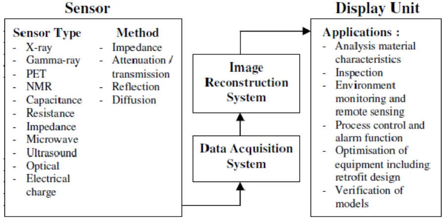
Fig. 1: Tomography System
In general, Tomography System consist four main sections which can be divide by sensor unit, data acquisition system, image reconstruction system and display unit as shown in Figure 1. Those units play their own major rules in Tomography System. A suitable type of sensor and processing technique can be selected based on the application to be used in system.
System Design:
Basically, DAS development divides into two sections; hardware and software implementation. Block diagram consist three main blocks; sensor unit, controller unit and display unit. Figure 2 shows overall system block diagram.
Controller unit must be able to read parallel output from sensor unit; sampling image and send it into a computer to be displayed in display unit. Embedded C programming language is used as a design coding. It has been written and compiled in Keil uVision4. Flash Magic is used to burn the hex file into microprocessor via Universal Serial Bus (USB) cable. In addition, this project involved three types of communication peripherals; Inter-Integrated Circuit (I2C), General Purpose Input/Output (GPIO) and Universal Asynchronous Receiver/ Transmitter (UART). Finally, the sample of data output will send to the computer and display on Graphical User Interface (GUI).
Hardware Design:
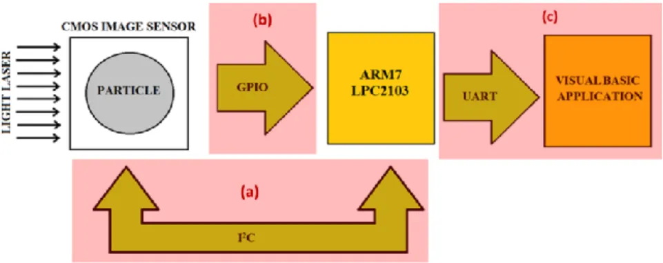
The aim of hardware design implementation is to achieve circuit designing with an appropriate hardware interfacing. Typical hardware design setting of DAS consist three main blocks; (a) sensor unit, (b) controller unit and (c) display unit. Those block can be illustrate in Figure 3.
Fig. 3: Overall Hardware Block Diagram
(a) Sensor Unit, (b) Controller Unit, (c) Display Unit
The works of hardware design falls under three headings:
1. Sensor Units:
The first block of hardware design; Sensor Unit, is responsible to detect shadow of the particle and convert it into a digital output. Light laser will supply a monochrome light source while the optical CMOS Image Sensor converts the light intensity from light laser and produce 10-bits of parallel digitized data output. There are two elements in sensor unit; light source and optical image sensor.
A. Light Laser:
The light laser properties divide into four main characteristics; monochromatic, directional, and coherent. The light laser emitting a monochromatic light source contain of one colour wavelength. In additional, the light emitted from the laser beam toward a relatively narrow will produce in one direction. Idroas, M., et al. says that laser produces a collimated beam approximately 1mm in diameter as shown in Figure 4 and proves that the laser emits a very high directional light (Idroas, M., et al. 2011a).
Fig. 4: Beam Produced by Laser (Idroas, M., et al. 2011a)
this research. Besides, laser has less aberration and will have a low error due to colour aberration. Thus, laser will be the best light source to get an accurate output result for this project.
B. Optical CMOS Image Sensor:
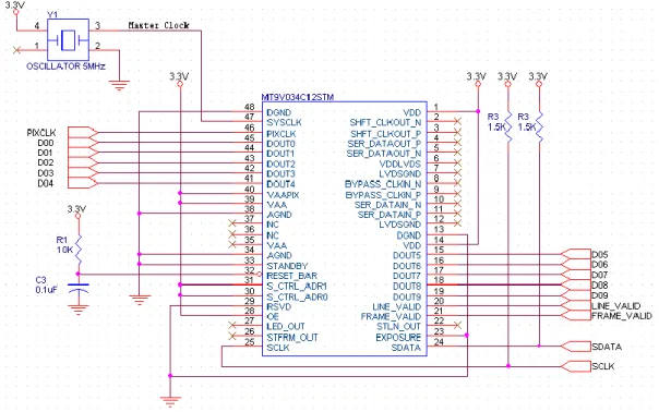
MT9V034C12STM series from APTINA Corp is chosen as an optical image sensor component in this project because of its monochrome and wide VGA format CMOS output format. MT9V034 has 752x480 active pixel arrays with 10-bits parallel digitize data output per pixel. It operates with 3.3±0.3V for every voltage supply. DigitalClarity feature in MT9V034 makes CMOS technology becomes a low noise image quality with keep it in lower cost and less than 160mW power consumptions.
MT9V034 comes in 48-CLCC packaging. It needs a 48-CLCC to 48-DIP adapter to make hardware interfacing become easier. Figure 5 shows 48 input output pins from CLCC adapter. There are several important pins need to be consider among those 48-pins. First pin at the left side of Figure 5 is the most important pin which connected to the master clock of the systems. This master clock will become a pixel clock for MT9V034 that synchronizes with all data output and can support master clock frequency until 27MHz.
1.5 KΩ resistor connected to SDATA and SCLK lines to pull the line up to VDD. Pull up circuits allow serial interface protocol to determine which device is pulling the line down. Internal MT9V034 register capacity has 16-bits wide. This register can be accessed through 16-bits or 8-bits two-wire serial interface sequences. Those remaining MT9V034 input output pin description will discussed in detail on Software Design section.
Fig. 5: MT9V034 Input Output Pin
2. Controller Unit:
Following that, the main controller unit can be acts as a brain of the system. Its responsibility is to process incoming data signal, sampling image output and producing necessary results. It also handles the communication peripherals between sensor unit and display unit. This research attempted to accomplish by using only a single embedded system as a controller unit to reduce overall project cost.
Controller unit used in this project is LPC2103 which develop based on ARM7TDMI-S CPU architecture from NXP Inc. LPC2103 UNO32 development board operates by 5V Direct Current (DC) powered from USB cable. LPC2103 comprises in several built-in peripherals such as GPIO, I2C, UART, SPI (Serial Peripheral Interface), ADC (Analogue-to-Digital Converter) and RTC (Real Time Clock). It generally driven by a 32 MHz external crystal oscillator, which delivers 8 MHz of the main clock (external clock is divided by four).
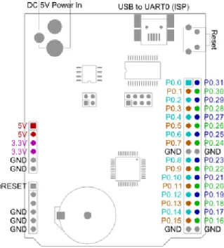
Fig. 6: LPC2103 UNO32 Input Output Pin
Besides, Figure 7 shows LPC2103 pin configurations. P0.0 and P0.1 are special reserved to UART and I2C peripherals. While, P0.24 until P0.25 connected to LINE_VALID, FRAME_VALID and PIXCLK image sensor. The remaining P0.16 until P0.23 used for DOUT from image sensor.
Fig. 7: LPC2103 UNO32 Pin Configuration
3. Display Unit:
Results from data sampling will be displayed on Visual Basic application which is the third block in hardware design. Universal Asynchronous Receiver/ Transmitter (UART) ports will be used in order to communicate between microprocessor with computer. But, for LPC2103 UNO 32 development board added chip FT232R to provide UART to USB converter. This latest technology performs a good security by burning a unique number into each device during assemble. This unique number performs a basic security to protect the data from being copied. LPC2103 UART port consists of P0.0 as RX1 and P0.1 as TX1. This port will be connected to FT232R port. This chip will convert UART to USB and straight away connect to computer using USB cable. This chip replaced the old tradition MAX232.
Software Design:
Fig. 8: Overall Software Block Diagram (a) GPIO, (b) UART, (c) I2C
1. MT9V034 I2C Protocol :
There are two type of I2C peripheral implementation which is 16-bit sequence and 8-bits sequences. Two-wired serial interface bus using 16-bits sequences have been chosen because of more simple and easy to apply. There are few difference codes to define serial interface protocol which can be shown as follows:
Table 1: I2C Protocol Codes
Pin Descriptions
Start Bit Master generates HIGH-to-LOW signal transition in positive edge triggered. Slave Address S_CTRL_ADR0 and S_CTRL_ADR1 pin used to determine four possible addresses. Acknowledge Bit (ACK) The master generates ACK pulse to make slave release the data line.
NoAcknowledge Bit (NACK) The NACK is generated to terminate a read sequence.
Stop Bit Master generates LOW-to-HIGH signal transition in positive edge triggered.
First sequence needs to be sent by master to enable serial interface bus is a combination between Start Bit, Slave Address and Write/Read Bit (S+ADDR+W/R). As mention before; to generate Start Bit master has to pulse HIGH-to-LOW signal. Besides, Slave Address and be determined by S_CTRL_ADR0 and S_CTRL_ADR1 pin.
Table 2 shows four possible Slave Addresses in MT9V034. For this project, S_CTRL_ADR0 and S_CTRL_ADR1 are connected to VDD. Thus, combination of 0xB8 used to send as a first sequence. Then, followed by the last bit of Write or Read signal which indicates by 0 and 1.
Table 2: MT9V034 Slave Addresses
{S_CTRL_ADR1, S_CTRL_ADR0} Descriptions Write/Read Mode
00
0x90 Write
0x91 Read
01
0x98 Write
0x99 Read
10
0xB0 Write
0xB1 Read
11
0xB8 Write
0xB9 Read
Figure 9 illustrates sequence of writing 16-bit data; 0x0284, into register R0x09. At the beginning of data transmission, master sending 8-bits combination of Start bit, Slave Address and write signal (S+ADDR+W = 0xB8) to image sensor. Next, wait until get an ACK from image sensor. ACK will only generated by image sensor if this combination matches with its internal address. After gets an ACK, register address (R0x09) will be sent to image sensor waits for another ACK. This step repeated to send MSB (0x02) and followed by LSB (0x84) data value. After that, STOP bit will be generated. After transferring 16-bits of register value into a preferred register, the register address will automatically updated with a new value. Master terminates the communication by sending a Stop signal.
2. MT9V034 Image Pixel Sampling:
Master clock from MT9V034 must synchronized with 1/4 clock from microprocessor. In this project, LPC2103 holds 32MHz value from its external clock (crystal). It will generate 8 MHz clock frequency which 1/4 clock from its external clock. Thus, an external oscillator will generate 5MHz clock to SYSCLK pin which is less than 8MHz. Generally, MT9V034 generates four types of data output; PIXCLK, LINE_VALID, FRAME_VALID and DOUT.
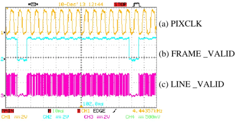
Technically, PIXCLK is a reversed version of the sensor master clock. LINE_VALID can represent by an indicator of row pixel. One complete LINE_VALID cycle means one row of image data pixel is completely generated. Besides, PIXCLK is synchronized with 10-bits parallel output pixels. A pixel of data output that contain in 10-bits DOUT will generated when LINE_VALID is HIGH. One by one output pixel will be generated in every single PIXCLK period. This output signal clearly shown in oscilloscope on Figure 10.
Fig. 10: Output MT9V034 Signal from Oscilloscope
MT9V032 generates 10-bits of parallel data output (DOUT9 to DOUT0) in every PIXCLK cycle. This project takes the most 8 significant bits; DOUT2 to DOUT9 for data sampling. It is because; the 8-bits output data are easy to manipulate and implements the result through display unit. While the remaining synchronous output signals; PIXCLK, LINE_VALID and FRAME_VALID are directly connect to controller unit. There are two methods to read an output pixel; progressive scan and interlaced scan. By referring to Figure 11, valid pixel output only available when LINE_VALID is high. Otherwise, data output is in blanking condition. Active pixels are surrounded by the horizontal and vertical blanking as shown Figure 12.
Fig. 11: Timing Diagram for MT9V032 Output Pixel
Fig. 12: MT9V032 Active Pixels
(a) PIXCLK
(b) FRAME _VALID
3. MT9V034Image Display:
Graphic User Interface (GUI) simply can be developed using Visual Basic application. This tool provides a friendly user interface, understandable and easy to implement. Visual Basic supported serial communication between computer and controller unit. MSCOMM.DDL is a windows standard serial communication component that needs to be included in while doing design development. This component sets with MSComm.Settings = "115200, N, 8, 1" parameter. Figure 13 shows the Visual Basic design interface.
For COM Port selection menu, the selection menu is added for change comport easily. Time taken box shows how many second that system take to complete one cycle of process. System will start counting from clicking start button until a complete output pixel shown in image frame. Start button at the left side of figure is the button used to initiate image sampling. A character sends to controller once this button clicked. Visual Basic application will received the data and convert it into image form to view in image frame. Total of package received together with total of pixel will be display in the textbox.
Fig. 13: Visual Basic Application GUI
RESULT AND DISCUSSIONS
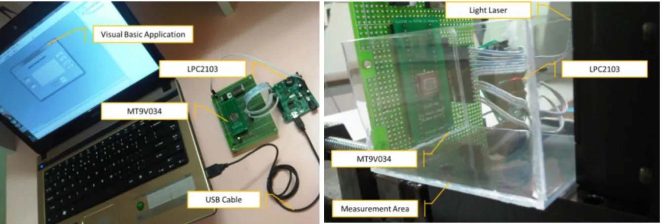
Basically, this experiment will test the sensor condition in two environments; normal lightening and using laser light as a light for CMOS image sensor. Thus, for the in a normal lightening environment, equipment will setting like Figure 14 (a) and Figure 14 (b) shows how to setting overall system in a light laser conditions.
Fig. 14: Data Acquisition System
(a) In Normal Lightening Environment (b) Using Laser Light Source
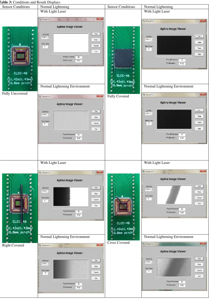
The important requirement in data acquisition system is to generate an accurate and avoid data lost during data sampling. There are several test cases need to be tested to ensure data acquisition meet this requirement. The verification has been done by displaying output image data into Visual Basic application. The experiments started with sensor fully uncovered condition, followed by checking row pixel, column pixel by placed a piece of black object across vertical and horizontal on image sensor.
Table 3: Conditions and Result Displays
Sensor Conditions Normal Lightening Sensor Conditions Normal Lightening
Fully Uncovered
With Light Laser
Fully Covered
With Light Laser
Normal Lightening Environment Normal Lightening Environment
Right Covered
With Light Laser
Cross Covered
With Light Laser
Normal Lightening Environment Normal Lightening Environment
Conclusions:
the system become expensive. This project comes with the main goal to develop a microprocessor-based data acquisition system for Optical Tomography. The specific objectives of the project have been fulfilled as below:
(a) System is designed as a low cost data acquisition system. Overall system is only cost USD80.75. This project has overcome the high price of data acquisition system in market.
(b) The designed microprocessor-based data acquisition system are able integrate with CMOS image sensor and display the output result in Visual Basic Application. The core unit in Optical Tomography System for obtaining accurate outputs is successfully developed.
ACKNOWLEDGEMENTS
The authors are grateful for the technical supports and contributions of Advanced Microprocessor Research Laboratory of University Teknologi Malaysia. Other individual whom I would like to thank is Assoc. Prof. Abdul Rahman bin Mohd from Universiti Malaysia Perlis for opinion and suggestions in handling problems faced during this research
REFERENCES
Dickin, F.J., B.S. Hoyle, A. Hunt, S.M. Huang, O. Ilyas, C. Lenn, R.C. Waterfall, R.A. Williams, C.G. Xie and M.S. Beck, 1992. Tomographic Imaging of Industrial Process Equipment: Techniques And Applications. Circuits, Devices and Systems, IEE Proceedings G. 139(1): 72-82.
Rahim, R.A. and R.G. Green, 1997. "A Review of Tomography Sensors and Applications." Journal Electrika.
Rahim, R.A., et al., 2005a. Tomographic imaging : Multiple fan beam projection technique using optical fibre sensors. in Computers, Communications, & Signal Processing with Special Track on Biomedical Engineering, 2005. CCSP 2005. 1st International Conference on.
Rahim, R.A., et al., 2005b. Data acquisition process in optical tomography : Signal sample and hold circuit. in Computers, Communications, & Signal Processing with Special Track on Biomedical Engineering, 2005.
CCSP 2005. 1st International Conference on.
Rahim, R.A., J.F. Pang, and K.S. Chan, 2005c. Optical tomography sensor configuration using two orthogonal and two rectilinear projection arrays. Flow Measurement and Instrumentation, 16(5): 327-340.
Rahim, R.A., 2005. High Speed Data Acquisition System for Computer Tomographic Imaging Instrumentation, PhD. Thesis, Universiti Teknologi Malaysia, Skudai.
Idroas, M., et al., 2011a. Modeling of A Charge Coupled Device Based Optical Tomographic Instrumentation System For Particle Sizing. Powder Technology, 212(1): 25-37.
Idroas, M., et al., 2011b. Optical tomography system based on charge-coupled device linear image sensors: Particle size measurement. Sensors and Actuators B: Chemical, 156(2): 572-577.
Dickin, F.J., B.S. Hoyle, A. Hunt, S.M. Huang, O. Ilyas, C. Lenn, R.C. Waterfall, R.A. Williams, C.G. Xie and M.S. Beck, 1992. Tomographic Imaging of Industrial Process Equipment: Techniques And Applications. Circuits, Devices and Systems, IEE Proceedings G. 139(1): 72-82.
Pang, J.F., R. Abdul Rahim and K.S. Chan, 2004. "Real time image reconstruction system using two data processing unit in optical tomography." Proceeding 3rd International Symposium on Process Tomography in Lodz, Poland.
Huang, Z. and H. Li., 2009. CMOS Sensor Sequences Designing of High-Speed Image Acquisition System Based on FPGA in Computational Intelligence and Software Engineering, 2009. CiSE 2009. International Conference.
Bei, Y., et al., 2011. Design of CMOS image acquisition system based on FPGA. in Industrial Electronics and Applications (ICIEA), 2011 6th IEEE Conference on.
Blanksby, A.J., et al., 1997. Noise performance of a color CMOS photogate image sensor. in Electron Devices Meeting, 1997. IEDM '97. Technical Digest., International.