Published online October 16, 2014 (http://www.sciencepublishinggroup.com/j/jeee) doi: 10.11648/j.jeee.s.2015030101.12
ISSN: 2329-1613 (Print); ISSN:2329-1605 (Online)
Open-loop voltage control voltage source inverter for a
linear load & non-linear load
Akhilesh Sharma
1, Neeraj Kumar
2, Gunjan Gupta
31
NERIST, Nirjuli, Arunachal Pradesh, India 2
DIET, Rishikesh, Uttarakhand, India 3
Invertis University, Bareilly, U.P., India
Email address:
[email protected] (A. Sharma), [email protected] (N. Kumar), [email protected] (G. Gupta)
To cite this article:
Akhilesh Sharma, Neeraj Kumar, Gunjan Gupta. Open-Loop Voltage Control Voltage Source Inverter for a Linear Load & Non-Linear Load.
Journal of Electrical and Electronic Engineering. Special Issue: Sustainable and Renewable Energies and Systems.
Vol. 3, No. 1-1, 2015, pp. 13-21. doi: 10.11648/j.jeee.s.2015030101.12
Abstract:
The conventional sources of energy are limited which are unable to meet the demand. There is always need of generation of electrical energy worldwide, may be in terms of few kilowatts to hundreds of kilowatts. The power requirement at the domestic level is terms of few kilowatts so there should be a way to meet the electrical demand at domestic level during load shading or fault. A subtitle to this could be a Voltage controlled voltage source inverters (VCVSIs). Now a day, such inverters are widely used in many applications like power supplies, power quality controllers, renewable energy, marine and military to meet the demand. Wherever an ac supply is need from a DC source, such inverters may be used. They are the heart and soul of converting DC into an ac source. Hence, such inverters should be designed so that they are robust and efficient. Inverter models can be design and simulated with software like Matlab Simulink to check suitability of inverter before implementing the hardware. Loads at the domestic level may be linear or non- linear hence a simple approach to design a voltage source inverter using open loop is presented in this paper.Keywords:
Voltage Controlled Voltage Source Inverters, MOSFET, Thyristors, Open-Loop Control System1. Introduction
Exponential growth of population and industries has lead to more demand of electrical power. The generating stations are unable to meet the power demand. Even the frequent power failure, hampers the living of people in cities, towns and villages. There is misbalance in utilization and generation of electrical power.
So it has become mandatory to switch engineers to find other alternative to meet so portion of the demand. Non- conventional sources have their own limitations. For example, solar power plant depends on factors like weather condition, altitude and solar radiation etc. If sky is clear, the places located at higher altitude will receive high intensity of solar radiation than the places located at low altitude during the day. The luminous intensity also varies from forenoon to afternoon. Hence, it is difficult to harness electrical energy from such sources at our will. One way to do so is to develop fast switching devices MOSFET, IGBT, BJT and Thyristors etc which help in converting DC into ac source called
inverter [1].
A fixed DC source can be converted to ac through an inverter. The function of an inverter is to change a fixed dc input to an ac output voltage of desired magnitude and frequency hence it can be said that the output voltage obtained from the device could be fixed or variable one without change in frequency. A variable output voltage can be obtained by varying the input dc voltage and maintaining the gain of the inverter constant. On the other hand, if the dc input voltage is fixed and it is not controllable, a variable output voltage can be obtained by varying the gain of the inverter, which is normally accomplished by pulse width modulation control within the inverter. [4 and 6].
forms may be accepted. In order to achieve sinusoidal wave of low distortion, the operating speed
semiconductor devices should be high. Further reduction in harmonic is possible if proper switching technique is applied. [1 and 5].
2. Principle of Operation of a Single
Phase
The principle of operation depends upon the switching of power electronic devices. Accordingly it
wave or full wave inverter. A half wave inver
requires two choppers whereas a full wave inverter requires four choppers. The former is discussed as under [
2.1. Half-Wave Inverter
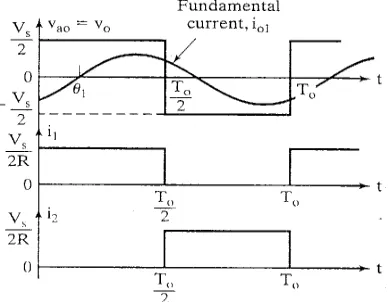
The principle of single phase half wave explained on the basis of figure 1 as under:
Figure 1. A single phase half wave inverter
A single phase half wave inverter consists of two choppers, say IGBTs in this case. When only one IGBT
for a time T0/2, the instantaneous voltage across the load v
Vs/2. If only the IGBT Q2 is turned on for a time T
appears across the load. The logic circuit should be designed in such a way that both the IGBTs do not turn at a time i.e. if Q1 turn on, Q2 should be off and vice –versa
the wave forms for the output voltage and resistive load.
Figure 2. Voltage and current waveform with resistive load
In order to achieve sinusoidal wave speed of power should be high. Further reduction in roper switching technique is applied.
of Operation of a Single
The principle of operation depends upon the switching of tronic devices. Accordingly it can either be half A half wave inverter is one which requires two choppers whereas a full wave inverter requires
under [1 and 6].
half wave inverters is
A single phase half wave inverter
A single phase half wave inverter consists of two choppers, IGBT Q1 is turned on
/2, the instantaneous voltage across the load v0 is
is turned on for a time T0/2, - Vs/2
appears across the load. The logic circuit should be designed s do not turn at a time i.e. if versa. Figure 2 shows he output voltage and currents with
Voltage and current waveform with resistive load
The root- mean- square (rms) output voltage can be found from
V dt
The instantaneous output voltage can be expressed in Fourier series as
2 cos
1!"#$%
2
&'
( )*+
which gives the instantaneous output voltage
∑ -.
/ ∞
,1,2… sin
where ) 2 6is the frequency of output voltage in radians per second. Due to the quarter wave symmetry of the output voltage along the x- axis, the even harmonics voltages are absent. The fundamental component of the
voltage is obtained for n=1, so equation (2.2
$ -.
√ / 0.45$
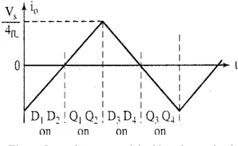
For a highly inductive load, the load immediately with the output voltage i.e. i
* <, the load current would continue to flow through D load, and lower half of the dc source until the current falls to zero. Similarly, when Q2 is turned off at
current flows through D1, load, and upper half of the dc
source. When either of the diode D
fed back to the dc source and these diodes are known as feedback diodes. Figure 3 shows the load current and conduction intervals of the device for a purely inductive load.
Figure 3. Current waveform
IGBTs can be replaced by any other switching devices like MOSFET, BJT, etc as per the requirement.
off time of a device, there should
of td = (toff) between the outgoing device and triggering of the
next incoming device. Otherwise would result through the two devices. condition, the conduction time is reduced. conduction time of a device would
All practical devices require a certain turn off time.
square (rms) output voltage can be found
dt+ / (2,1)
voltage can be expressed in
>)*+ sin >)*++
"$2 ( )*+%
'
? @ @
A 4$%
>
which gives the instantaneous output voltage as
sin >)* 0 > 2,4,6 … (2.2)
s the frequency of output voltage in radians per second. Due to the quarter wave symmetry of the output axis, the even harmonics voltages are The fundamental component of the rms output
equation (2.2) reduces to
$% (2.3)
inductive load, the load current cannot change diately with the output voltage i.e. if Q1 is turned off at
current would continue to flow through D2,
load, and lower half of the dc source until the current falls to is turned off at * D , the load , load, and upper half of the dc diode D1 or D2 conducts, energy is
fed back to the dc source and these diodes are known as shows the load current and conduction intervals of the device for a purely inductive load.
Current waveform with inductive load
can be replaced by any other switching devices like , etc as per the requirement. If toff is the turn
should be a minimum delay time ) between the outgoing device and triggering of the g device. Otherwise, short circuit condition would result through the two devices. In order to avoid this condition, the conduction time is reduced. The maximum conduction time of a device would be tEF # tG.
2.2. Principle of Operation of a Full-Wave Inverter
A single phase bridge voltage source inver shown in figure 4. It consists of four choppers. When Q1 and Q2 are turned on simultaneously, the input voltage Vs
appears across the load. If IGBTs Q3 and Q
the same time, the voltage across the load is reversed and is Vs. the wave for the output voltage is shown in figure
Figure 4. A single phase full wave inverter
Table 1. Switch State for Single Phase Full Voltage Source Inverter (VSI)
State State No.
S1, and S2 are on and S4, and S3 are off 1
S4, and S3 are on and S1, and S2 are off 2
S1, and S3 are on and S4, and S2 are off 3
S4, and S2 are on and S1, and S3 are off 4
S1, S2 S3 and S4 all are off 5
The fundamental rms component of the output voltage is obtained by substituting n=1. Therefore the fundamental voltage is
$ -.
√ / 0.90$%
3. Simulation
The entire simulation has been carried out in MATLAB 7.0.1 SIMULINK. Both linear and non linear loa
considered for open loop control of voltage controlled voltage source inverter. The parameters of the in
given in table 2 [2].
Wave Single Phase
A single phase bridge voltage source inverter (VSI) is . It consists of four choppers. When IGBTs are turned on simultaneously, the input voltage Vs and Q4 are turned on at
the same time, the voltage across the load is reversed and is – t voltage is shown in figure 5.
ase full wave inverter
Figure 5. Load current with highly inductive load
Table 1 shows the five switch states. figure 4 act as the switching devices S
two switches: one upper and one lower conduct at the same time such that the output voltage is
whereas if these switches are off at the same time, the switch state is 0. Figure 5 shows the load current for highly inductive load.
The rms output voltage can be found from as under
V VI dt+
Equation 2.2 can be extended to express the instantaneous output voltage in a Fourier series as
∑ -.
/
,1,2… sin
Switch State for Single Phase Full Voltage Source Inverter (VSI)
State No. Switch State JKL JML JL
10 $%
2
#$%
2 $%
01 $%
2 #$2% $%
11 $%
2 $2% 0
00 #$%
2 #$% 2 0 Off #$% 2 $% 2 $% 2 #$% 2 #$% $%
component of the output voltage is obtained by substituting n=1. Therefore the fundamental
(2.6)
been carried out in MATLAB SIMULINK. Both linear and non linear loads have been of voltage controlled voltage source inverter. The parameters of the inverter are
Table 2.Parameters of Inverter
PARAMETER LABEL
Rated power
-Rated output frequency F
Rated output voltage V
Battery voltage V
Battery and lead wire resistance R
DC filter capacitance C
Inverter Switching frequency f
Filter inductor L
Filter inductor Resistance R
Transformer turns ratio N
The Matlab Simulink model of the single control voltage source inverter is shown in Figure
current with highly inductive load
1 shows the five switch states. IGBTs Q1, Q4 in
act as the switching devices S1, S4, respectively. If
two switches: one upper and one lower conduct at the same such that the output voltage isN$%, the switch state is 1, whereas if these switches are off at the same time, the switch shows the load current for highly
The rms output voltage can be found from the expression
+ / V
I (2.4)
Equation 2.2 can be extended to express the instantaneous output voltage in a Fourier series as
sin >)* (2.5)
Component Conducting
S1, and S2 if i0>0 D1 and D2 if i0<0
D4 and D3 if i0>0 S4 and S3 if i0<0
S1 and D3 if i0>0 D1 and S3 if i0<0
D4 and S2 if i0>0 S4 and D2 if i0<0
D4 and D3 if i0>0 S4 and S3 if i0<0
Parameters of Inverter
LABEL VALUE UNIT
3.5 kVA
Fload 50 Hz
Vload 230 V
Vbatt 24 V
Rbatt 30 mΩ
Cdc 4 mF
fsw 20 kHz
Lf 1 µH
RLf 1 µΩ
N 18 ---
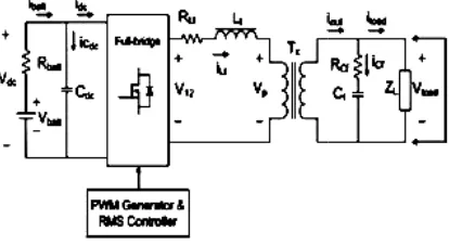
model developed using the Simulink power system blockset, comprises of components such as power electronic devices (full-bridge and rectifier) and elements such as inductors, capacitors and resistors. The DC model used comprises of the battery (Vbatt) and its respective resistance and lead wire
resistance (Rbatt) as well as the filter capacitor (C
bus current measurement resistor (Idc measure), which is of
the order of micro-ohms as it is only used for DC bus current measurement. The output from the full
comprises of the filter inductor and its resistance (L filter capacitor with damping resistor (Cf, R
is the step-up transformer (Tx). The resistor ‘R
order of micro-ohms and is only used for load current measurement which is similar to ‘Idc measure.
Figure 6. Physical components of single phase VCVSI
A system model showing the physical components of the single-phase Voltage controlled voltage source inverter modeled using Matlab Simulink is shown in Figure model developed using the Simulink power system blockset,
of components such as power electronic devices bridge and rectifier) and elements such as inductors, capacitors and resistors. The DC model used comprises of the ) and its respective resistance and lead wire s the filter capacitor (Cdc) and a DC
measure), which is of ohms as it is only used for DC bus current measurement. The output from the full-bridge block stance (Lf, RLf) and
, RCf). Also included
). The resistor ‘Rmeasure’ is of the
ohms and is only used for load current measure.
phase VCVSI
A system model showing the physical components of the phase Voltage controlled voltage source inverter modeled using Matlab Simulink is shown in Figure 6. This
inverter uses a low-voltage DC bus (24V stepped up to 240VAC using a step
transformer provides galvanic isolation and is a simple solution for the stepping up of a low
DC bus in the model comprises of the battery (V wire and battery resistance (R
(Cdc). The full-bridge uses IGBT switching devices with the
full-bridge output filtered using a low
Cf). The inductor filter resistance is represented as R
the LC filter-damping resistor being R
to the inverter (ZL) is considered arbitrary (linear and/or non
linear).
The PWM generator provides the switching signals f full-bridge. The inverter system modeled with Matlab Simulink was achieved using the power system and standard simulink blocksets. The system was analyzed by sending the required signal to scopes and the workspace, which allowed for analysis and design of the inverter model. The PWM signals for each of the power ele
bridge come from the PWM generator block. This block allows for the switching frequency and number of inverter legs to be selected with all PWM signal multiplexed on a single bus into the full-bridge block (pulses). The input to this block (signal(s)) is the sinusoidal reference for the inverter. For the open-loop control, t
(sinusoidal reference) is generated from a generator in Simulink. The simulink model
linear load and a non-linear load figure 8 respectively [2 and 3].
Figure 7. Simulink Model for linear load
Figure 8. Simulink Model for non-linear load
voltage DC bus (24VDC), which is
stepped up to 240VAC using a step-up transformer (Tx). The
transformer provides galvanic isolation and is a simple solution for the stepping up of a low-voltage DC bus. The DC bus in the model comprises of the battery (Vbatt), lead
attery resistance (Rbatt), and DC filter capacitor
bridge uses IGBT switching devices with the bridge output filtered using a low-pass LC filter (Lf and
). The inductor filter resistance is represented as RLf with
ng resistor being RCf. The load connected
) is considered arbitrary (linear and/or
4. Results
The simulation results for liner and non been obtained and are shown in figures.
4.1. Linear Load
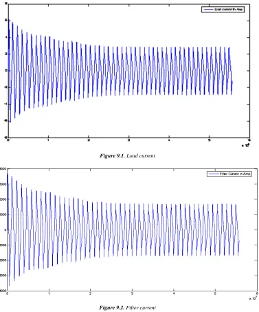
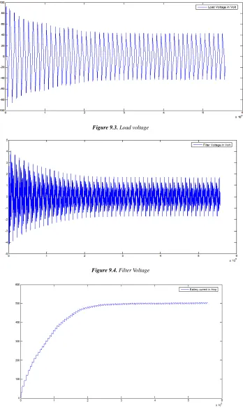
Figures 9.1, 9.2, 9.3, 9.4 and 9.5 are the simulation results of the Voltage Controlled Voltage Source Inverter with open loop control having a linear load of 3.5 kVA
9.1, initially, the load current is maximum, about 6.2 A settles around 4 A after 0.33 seconds. The maximum load voltage is 90V and it decreases until it settles d
simulation results for liner and non-linear loads have
are the simulation results of the Voltage Controlled Voltage Source Inverter with open a linear load of 3.5 kVA. From the figure urrent is maximum, about 6.2 A and after 0.33 seconds. The maximum load voltage is 90V and it decreases until it settles down at 60V as
seen in figure 9.2. The filter cu
about 3700 A initially and settles around 2000 A
filter current is due to too small impedance offered by the filter inductor Lf as seen in figure 9.3
shown in figure 9.4. The maximum filter vo initially. It settles to 2V after 0.33 second. The bat settles at 500 A, starting from zero
the beginning, when the inverter is switched on, the battery current starts building up. Because of the presence
the circuit, battery current settles to 500 A
Both, load current and load voltage are similar, except the amplitudes.
Figure 9.1. Load current
Figure 9.2. Filter current
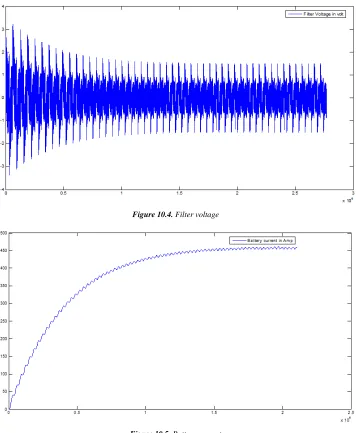
4.2. Non-Linear Load
The various plots obtained through open loop control of a non-linear load are shown in figure 10.1, 10.2, 10.3, 10.4 and 10.5 respectively. As it is seen from the figure 10.1
current waveform is not sinusoidal as was in the case of linear load where both load current and load voltage were
Figure 9.3. Load voltage
Figure 9.4. Filter Voltage
Figure 9.5. Battery current
The various plots obtained through open loop control of a ear load are shown in figure 10.1, 10.2, 10.3, 10.4 and igure 10.1 that the current waveform is not sinusoidal as was in the case of linear load where both load current and load voltage were
similar. It is due to non-linearity in the load, hence current wave form is not a complete sinusoidal. The amplitude of the load current becomes constant after 0.03 seconds and is about 1.26 Amps. The amplitude of the voltage
in figure 10.2. The steady amplitu and maximum amplitude of the
figure 10.3. The filter amplitude of voltage is small nearly about 2V and the battery current rises from zero to 450 A in
0.05 seconds as seen in figure 10.4 and figure 10.5 respectively.
Figure 10.1. Load current
Figure 10.2. Load voltage
Figure 10.4. Filter voltage
Figure 10.5. Battery current
5. Conclusions
A Matlab Simulink model of a single-phase 3.5 kVA Voltage Controlled Voltage Source Inverter with open-loop control has been developed for linear and non-linear loads.
When the nature of load is purely linear, the load current has constant frequency and amplitude after 0.33 sec but this is not so in case of non-linear load, where the load current is not sinusoidal with constant amplitude although there is decrease in steady time. When the load is non-linear, the filter current decreases. There is also decrease of as source current, thus allow to use non-linear load. Irrespective of the nature of load, the filter voltage in both cases is independent of the load current. So it can be concluded that for a open loop system, the non-linear load is preferred.
About the Authors
Akhilesh Sharma is working as Assist. Prof. in North
Eastern Regional Institute of Science and Technology (under Ministry of Human Resource & Development, Govt of India), Nirjuli, Arunachal Pradesh, India in electrical engineering department. He did his Master’s degree in Power Electronics & Drives from Madan Mohan Malaviya Engineering College Gorakhpur in 2009 under Uttar Pradesh Technical University, Lucknow, Uttar Pradesh, India.. His area of interest is Neural Networks, Inverter and Electric Drives.
Neeraj Kumar has done post graduation in electrical engineering from Madan Mohan Malaviya Engineering College Gorakhpur in 2009 under Uttar Pradesh Technical University, Lucknow, Uttar Pradesh, India. He is working as Associate professor in DIET, Rishikesh, under Uttarakhand Technical University, Dehradun, Uttarakhand, India. His field of research includes electric drives and control.
References
[1] N. Mohan, T. M. Undeland, and W. P. Robbins, Power Electronics - Converters, Applications, and Design, 2nd ed: John Wiley & Sons, Inc., 1995.
[2] "Matlab 6, Release 12.1." Natick, Massachusetts: The MathWorks (www.mathworks.com), 2006. "PSIM Version 7.0." Woburn, MA: Powersim Inc. (www.powersimtech.com), 2006.
[3] M. Trigg, "Digital Sinusoidal PWM Generation using a Low-cost Micro-controller Based Single-Phase Inverter," presented at ETFA 2005, Catania, Italy, 2005.
[4] M. C. Trigg, H. Dehbonei, and C. V. Nayar, "Digital Sinusoidal PWMs for a Microcontroller based Single-Phase Inverter. Part 1: Principles of digital sinusoidal PWM generation," IJE Power electronics and instrumentation hardware, 2005.
[5] H. Dehbonei, M. C. Trigg, and C. Nayar, "A Novel Sinewave Inverter for Harsh Environment," presented at AUPEC 2005, Hobart, Tasmania, Australia, 2005.