Vol. 4, Issue 1, January 2015
A High Step up Boost Converter Using
Coupled Inductor with PI Control
Saurabh1, Dr.P.K.Saha2, Dr.G.K.Panda3
PG Student [Power Electronics and Drives], Dept. of EE, Jalpaiguri Government Engineering College, Jalpaiguri,
West Bengal, India 1
Professor, Dept. of EE, Jalpaiguri Government Engineering College, Jalpaiguri, West Bengal, India 2
Professor and HOD, Dept. of EE, Jalpaiguri Government Engineering College, Jalpaiguri, West Bengal, India 3
ABSTRACT:The paper proposes a high step up boost converter. The proposed converter has used a coupled inductor with switched capacitors. The capacitors were made to get charged in parallel and were made to get discharged in series by the configuration to achieve high step up voltage gain. And the voltage across the load is maintained constant by using a closed loop control.
The operation and steady state analysis of the configuration has been shown in detail. Finally, a circuit with 24-V input, 400-V output, and power of 200W has been implemented in MATLAB software to verify the proper working and performance of the proposed configuration.
KEYWORDS: High step-up Boost Converter, Coupled Inductor, Switched Capacitor, PI Controller.
I.INTRODUCTION
Boost converter is one of the most important and widely used devices of modern power applications.These converters are electronic devices used to change DC electrical power efficiently from one voltage level to another. They provide smooth acceleration control, high efficiency, and fast dynamic response. There are FOUR main types of converter usually called the buck, boost, buck-boost and Boost converters. The buck converter is used for voltage step-down/reduction, while the boost converter is used for voltage step-up. The buck-boost and Cuk converters can be used for either step-down or step-up.
Basically, the DC-DC converter consists of the power semiconductor devices which are operated as electronic switches and classified as switched-mode DC-DC converters. Operation of the switching devices causes the inherently nonlinear characteristic of the DC-DC converters. Due to this unwanted nonlinear characteristics, the converters requires a controller with a high degree of dynamic response. Pulse Width Modulation (PWM) is the most frequently consider method among the various switching control method. In DC-DC voltage regulators, it is important to supply a constant output voltage, regardless of disturbances on the input voltage.
Nowadays, the control systems for many power electronic appliances have been increasing widely. Crucial with these demands, many researchers or designers have been struggling to find the most economic and reliable controller to meet these demands. The idea to have a control system in dc-dc converter is to ensure desired voltage output can be produced efficiently as compared to open loop system. Controller for the PWM switching control is done by Proportional-Integral (PI) controller.
Vol. 4, Issue 1, January 2015
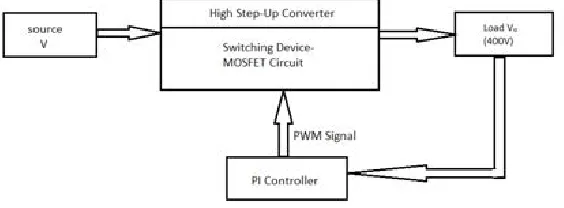
Figure 1 shows the block diagram of the proposed converter with closed loop control such that the voltage drift problem is minimized and the desired output is maintained. The output voltage was then taken as feedback and compared with desired value of output voltage and the difference is then fed to PI control which then produces the PWM signal to the switch of the converter.
Figure 1 Proposed block diagram
II.SYSTEM MODEL AND ASSUMPTIONS
Figure 2 shows the configuration of the proposed circuit. The circuit has a boost converter with coupled inductor, switched capacitor and a clamp circuit. The equivalent circuit of the coupled inductor consists of a magnetizing inductor Lm, leakage Lk, and an ideal transformer. The leakage inductor energy of the coupled inductor is recycled to capacitor C1, and thus the voltage across the switch S can be clamped. The voltage across the capacitors C2, and C3 can be adjusted by the turns ratio of the coupled inductor. For these reasons the voltage of switch is reduced significantly and low conducting resistance Rds(on) of the switch can be used. Thus high step-up voltage gain can be achieved.
Figure 2 Circuit configuration of the proposed converter
To simplify the circuit analysis, these conditions have been assumed.
A. Capacitors C1, C2, C3 and C0 are very large which makes voltages VC1, VC2, VC3 and VO to be constant in one switching period.
B. The power devices used are ideal, but the parasitic capacitance of the power switch was considered.
Vol. 4, Issue 1, January 2015
III.MODES OF OPERATION AND ANALYSIS
There are five operating modes in one switching period.
1) Mode I (t0, t1): Mode will start when the switch S is turned ON. Diodes D1 and D0 are off, and D2 and D3 are on. The current through Lk starts increasing linearly. The inductor Lm starts storing energy from the source voltage. Voltages VC2 and VC3 being connected in series to charge the output capacitor CO which will then provide energy to the load. When current through D0 becomes zero, operating mode ends.
2) Mode II (t1, t2): Here S will be kept ON. Diodes D1, D2 and D3 are off and D0 is on. The Lm starts getting charged due to the source voltage. Capacitors C2 and C3 are also get charged due to the source via the coupled inductor. Capacitor C0 discharges to the load to maintain the desired output voltage. Switch S turns off to end the mode.
3) Mode III (t2, t3): S is turned OFF in this mode. Diodes D1, D2 and D3 are off, and D0 is on. Inductors Lk and Lm are discharged to the parasitic capacitor of the switch Cds. Capacitor CO continues to discharge and to provide energy to the load. Now the voltage across C1 is equal to Vin+Vds, diode D1 now turned on and the mode ends.
4) Mode IV (t3, t4): S is kept OFF. Diodes D1 and D0 are turned on and D2 and D3 are off. Inductors Lk and Lm are discharged to charge capacitor C1. Lk gets discharged quickly. No current flows through the secondary side and L2 charges capacitor C0 and maintains the voltage across the load, which makes D0 to switch off and mode ends.
5) Mode V (t4, t5): S is kept OFF. Diodes D1, D2 and D3 are turned on and D0 is turned off. Inductors Lk and Lm are discharged to charge capacitor C1. Making the voltage across the switch equals Vin+VC1. And L2 is charging both the capacitors C2 and C3. The mode ends when the switch is turned ON and makes the next switching period.
IV.SIMULATION RESULTS AND DISCUSSIONS
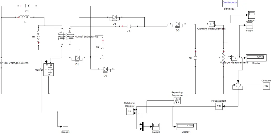
Figure 3 shows the MATLAB Simulation diagram of a high step-up boost converter using coupled inductor with PI control. The duty ratio of the switch is adjusted by PI Controller to obtain the require output.
Figure 3 MATLAB Simulation Diagram of proposed converter with PI controller.
Vol. 4, Issue 1, January 2015
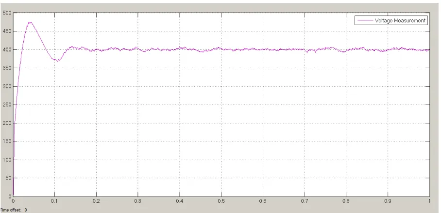
Figure 4 Output voltage (V0=400.3V).
Figure 5 shows the output current of 0.5A which shows the proposed controller was well able to control the output current as desired.
Figure 5 Output Current (I0=0.5A).
Vol. 4, Issue 1, January 2015
Figure 6 Pulse generated by PI controller for the switch.
Vol. 4, Issue 1, January 2015
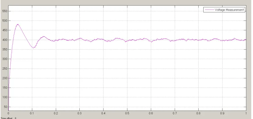
From Figure 7 it is very much clear and can be calculated that the output voltage VO is not much stable with KP=0.009 and KI=1.1, 1.2, 1.3, 1.5 and the maximum peak overshoot, rise time is also more than the output in Figure 4. The output voltage waveform shown in Figure 4 has less settling time. Hence, we have chosen the values for KP and KI as in serial number 4 from the table i.e. KP=0.009 and KI=1.4. While the converter specifications were kept same.
V.CONCLUSION
Here a high step-up boost converter using coupled inductor with proportional integral control is simulated. By the capacitor charged in parallel and discharged in series by the coupled inductor, high step-up voltage gain of 400V is achieved. As the output voltage of the converter with PI Control has minimum overshoot and produces a constant output current shown. These studies could solve many types of problems regardless on stability because as we know that proportional integral controller is an intelligent controller to their appliances.
Further it can be simulated with different types of feedback control like fuzzy logic control, artificial neural network, genetic algorithm and others can be used for advanced tuning and to check the constant output voltage with least ripple and to support different appliances with different voltage ratings.
REFERENCES
1. Y.P. Hsieh, J.F Chen, T.J Liangand L.S. Yang, “Novel High Step-Up DC–DC Converter with Coupled-Inductor and Switched-Capacitor Techniques for a Sustainable Energy System”,IEEE Trans. Power Electron.,vol. 26, no. 12, Dec 2011.
2. R. J. Wai and R. Y. Duan, “High step-up converter with coupled inductor,” IEEE Trans. Power Electron., vol. 20, no. 5, pp. 1025–1035, Sep. 2005.
3. S.K. Changchien, T.J Liang, J.F. Chen and L.S. Yang, “Novel High Step-Up DC–DC Converter for Fuel Cell Energy Conversion System”, IEEE Trans Ind. Electron., vol. 57, no. 6, June 2010.
4. Q. Zhao and F. C. Lee, “High-efficiency, high step-up dc–dc converters,” IEEE Trans. Power Electron., vol. 18, no. 1, pp. 65– 73, Jan. 2003. 5. T.J. Liang, S.M. Chen, L.S Yang, J.F. Chen, and A. Ioinovici, “Ultra-Large Gain Step-Up Switched-Capacitor DC-DC Converter With Coupled
Inductor for Alternative Sources of Energy”, IEEE Trans Circuits And Systems—I: Regular Papers, vol. 59, no. 4, Apr 2012.
6. F.H. Dupont, C. Rech, R. Gules and J. R. Pinheiro, “Reduced- Order Model and Control Approach for the Boost Converter With a Voltage Multiplier Cell”, IEEETrans Power Electron.,vol. 28, no. 7, July 2013.
7. Rashid M.H., “Power Electronics Handbook”, Academic press, New York, 2001.
BIOGRAPHY
Saurabh was born in Jharkhand, India on January 15, 1990. He received his B.Tech degree in Electronics and Instrumentation Engineering from Bharath University, Chennai in 2011, and currently he is doing M.Tech degree in Power Electronics and Drives from Jalpaiguri Government Engineering College, Jalpaiguri, West Bengal.
Prof. Pradip Kumar Saha, Professor, Department of Electrical Engineering, Jalpaiguri Government Engineering College, Jalpaiguri, WB -735102. BE (Electrical) from B.E. College, Shibpore. M.Tech (Electrical) Specialization: Machine Drives & Power Electronics from IIT- Kharagpur, PhD from University of North Bengal. FIE, MISTE, Certified Energy Auditor.