P a g e | 1457
Design of Redundant Binary Multipliers using Modified Partial
Product Generator
1
P.Harikrishna.
M.Tech.
2
Mrs.M.Pavitra
Associate Professor.
1,2
Dept of ECE (VLSID). 1,2
PBR VITS College of Engineering, Kavali, Andhra Pradesh .
Abstract: Multiplication is one of the
basic functions used in digital signal processing (DSP). Due to its high modularity and carry-free addition, a redundant binary (RB) representation can be used when designing high performance multipliers. The conventional RB multiplier requires an additional RB partial product (RBPP) row, because an error-correcting word (ECW) is generated by both the radix-4 Modified Booth encoding (MBE) and the RB encoding.
This incurs in an additional RBPP accumulation stage for the MBE multiplier. In this paper, a new RB modified partial product generator (RBMPPG) is proposed; it removes the extra ECW and hence, it saves one RBPP accumulation stage. Therefore, the proposed RBMPPG generates fewer partial product rows than a conventional RB MBE multiplier. Simulation results show that the proposed RBMPPG based designs significantly improve the area and High speed when the word length of each operand in the multiplier is at least 32 bits; these reductions over previous NB multiplier designs incur in
a modest delay increase. The delay can be reduced using the proposed RB multipliers when compared with existing RB multipliers.
Index Terms- Redundant binary modified booth encoding, RB partial product generator, RB multiplier.
1 INTRODUCTION
The redundant binary number representation has been introduced by Avizienis to perform signed-digit arithmetic; the RB number has the capability to be represented in different ways. Fast multipliers can be designed using redundant binary addition trees. The redundant binary representation has also been applied to a floating-point processor and implemented in VLSI. High performance RB multipliers have become popular due to the advantageous features, such as high modularity and carry-free addition.
A RB multiplier consists of a RB partial product (RBPP) generator, a RBPP reduction tree and a RB-NB converter. A Radix-4 Booth encoding or a modified Booth encoding (MBE) is usually used in the partial product generator of parallel multipliers to reduce the number of partial product rows by half. A RBPP row can be obtained from two adjacent NB partial product rows by inverting one of the pair rows an N-bit conventional RB MBE (CRBBE-2) multiplier requires [N/4] RBPP rows. An additional error-correcting word (ECW) is also required by both the RB and the Booth encoding therefore, the number of RBPP accumulation stages (NRBPPAS) required by a power-of-two word-length (i.e., 2n-bit) multiplier is given by:
(1)
If the additional ECW can be removed, an RBPP accumulation stage is saved, so resulting in improvements of complexity and critical path delay for a RB multiplier. For example, a conventional
32- bit RB multiplier has four RBPP accumulation stages; if the ECW is removed, then the number of RBPP accumulation stages is reduced to 3, i.e., the stage count is decreased by 25 percent. Note that the problem of extra ECW does not exist in standard significant size (i.e., 24x24-bit and 5454-bit) RB multipliers as used in floating point-arithmetic units.
Alternatively, a high-radix Booth encoding technique can reduce the number of partial products. However, the number of expensive hard multiples (i.e., a multiple that is not a power of two and the operation cannot be performed by simple shifting and/or complementation) increases too. Besli and Desmukh noticed that some hard multiples can be obtained by the differences of two simple power-of-two multiplies. A new radix-16 Booth encoding (RBBE-4) technique without ECW has been proposed in it avoids the issue of hard multiples. A radix-16 RB Booth encoder can be used to overcome the hard multiple problem and avoid the extra ECW, but at the cost of doubling the number of RBPP rows. Therefore, the number of radix-16 RBPP rows is the same as in the radix-4 MBE. However, the RBPP generator based on a radix-16 Booth encoding has a complex circuit structure and a lower speed compared with the MBE partial product generator when requiring the same number of partial products.
P a g e | 1459
generated by the last partial product row is combined with both the two most significant bits (MSBs) of the first partial product row and the two least significant bits (LSBs) of the last partial product row by logic simplification. Therefore, the proposed method reduces the number of RBPP rows from N=4 þ 1 to N=4, i.e., a RBPP accumulation stage is saved. The proposed method is applied to 8x8-, 16x16- and 32x32-bit RB multiplier designs; the designs are synthesized and simulated on Xilinx ISE. The proposed designs achieve significant reductions in compared with existing multipliers when the word length of each of the operands is at least 32 bits. While a modest increase in delay is encountered (approximately 5 percent).
This paper is organized as follows. Section 2 introduces radix-4 Booth encoding. The design of the conventional RBPP generator is also reviewed. Section 3 presents the proposed RBMPPG. This section also demonstrates the adoption of the proposed RBMPPG into various word-length RB multipliers. Section 4 provides the evaluation results of the new RB multipliers using the proposed RBMPPG for different word lengths and compares them to previous best designs found in the technical literature. The conclusion is provided in Section 5.
2. EXISTING BOOTH MULTIPLIER
2.1 Non-Redundant Radix-4 Signed-Digit Algorithm
Fig.2.1. Block diagram of the NR4SD encoding scheme at the (a) digit and (b) word level.
Fig.2.2. Block diagram of the NR4SDþ encoding scheme at the (a) digit and (b) word level.
Step1. Consider the initial values j =0 and c0 =0.
Step2. Calculate the carry c2j+1 and the sum n+2j of a half adder (HA) with inputs b2j and c2j (Fig.2.
Step3. Calculate the positively signed carry c2j+2 (+) and the negatively signed sum n 2j+1 (-) of a HA* with inputs b2j+1 (+) and c2j+1 (+) (Fig.3.1a). The outputs c2j+2 and n 2j+1 of the HA* relate to its inputs as follows:
The following Boolean equations summarize the HA* operation:
Step 4. Calculate the value of the bNR-j digit.
……. (2.5)
Equation (5) results from the fact that n
-2j+1 is negatively signed and n+2j is positively signed.
Step5. j :=j + 1.
Step6. If If (j < k_ 1), go to Step 2. If (j = k -1), encode the most significant digit based on the MB algorithm and considering the three consecutive bits to be b2k-1, b2k-2 and c2k-2 (Fig.2.1b). If (j = k), stop.
Equations (6) show how the NR4SD -encoding signals one+j, one-j and two-j of Table 2.2 are generated.
…….. (2.6)
The minimum and maximum limits of the
dynamic range in the NR4SD- form are
-2n-1 -2n-3 -2n-5 -…-2 < -2n-1 and 2n-1 +
2n-4 + 2n-6 +…. +1 > 2n-1 - 1. We
observe that the NR4SD- form has larger
dynamic range than the 2‘s complement form.
2.1.1 NR4SDþ Algorithm
Step1. Consider the initial values j = 0 and c0 =0.
Step2. Calculate the positively signed carry c2j+1 (+) and the negatively signed sum n-2j (-) of a HA* with inputs b2j (+) and c2j (+) (Fig. 2a). The carry
c2j+1 and the sum n-2j of the HA* relate to
its inputs as follows:
The outputs of the HA* are analyzed at gate level in the following equations:
Step3. Calculate the carry c2j+2 and the sum n+ 2j+1 of a HA with inputs b2j+1 and c2j+1.
Step4. Calculate the value of the bNR+ j digit
……. (2.7)
Step5. j := j + 1.
Step 6. If (j < k_-1), go to Step 2. If (j = k - 1), encode the most significant digit
according to MB algorithm and
considering the three consecutive bits to be b2k-1, b2k-2 and c2k-2 (Fig.2.2b). If (j =k), stop.
P a g e | 1461
….. (2.8) The minimum and maximum limits of the dynamic range in the NR4SDþ form are -2n-1 -2n-4 - 2n-6 -… -1 < -2n-1 and 2n-1 + 2n-3 + 2n-5 +…. +2 > 2n-1 - 1. As observed in the NR4SD_ encoding technique, the NR4SDþ form has larger dynamic range than the 2‘s complement form.
Considering the 8-bit 2‘s complement number N, Table 2.4 exposes the limit values -28 = -128, 28 - 1 = 127, and two typical values of N, and presents the MB, NR4SD_ and NR4SDþ digits that result
when applying the corresponding
encoding techniques to each value of N we considered. We added a bar above the negatively signed digits in order to distinguish them from the positively signed ones.
2.2 Pre-Encoded Multipliers Design:
In this section, we explore the implementation of pre-encoded multipliers. One of the two inputs of these multipliers is pre-encoded either in MB or in NR4SD-/NR4SD+ representation. We consider that this input comes from a set of fixed coefficients (e.g., the coefficients for a number of filters in which this multiplier will be used in a dedicated system or the sine table required in an FFT implementation).The coefficients are encoded off-line based on MB or NR4SD algorithms and the resulting bits of encoding are stored in a ROM. Since our purpose is to estimate the efficiency of
the proposed multipliers, we first present a review of the conventional MB multiplier in order to compare it with the pre-encoded schemes.
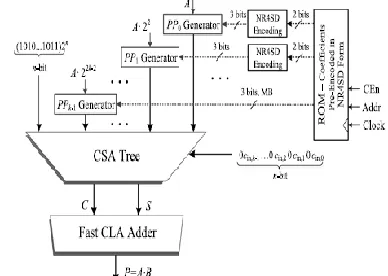
Fig.2.3. System architecture of the conventional MB multiplier.
2.2.1 Conventional MB Multiplier:
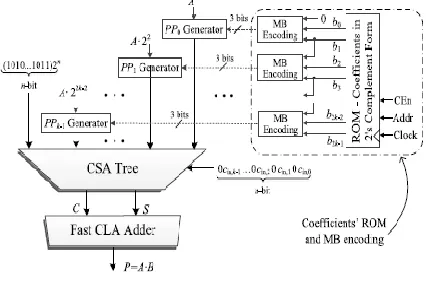
Fig. 2.3 presents the architecture of the system which comprises the conventional MB multiplier and the ROM with coefficients in 2‘s complement form. Let us consider the multiplication A •B. The coefficient B =(bn_1 . . . b0)2‘s consists of n = 2k bits and is driven to the MB encoding blocks from a ROM where it is stored in 2‘s complement form. It is encoded according to the MB algorithm (Section 2) and multiplied by A =(an_1 . . .
a0)2‘s, which is in 2‘s complement
representation. We note that the ROM data bus width equals the width of coefficient B (n bits) and that it outputs one coefficient on each clock cycle. The k partial products are generated as follows:
…….. (2.9)
of the least and most significant bits of PPj , we consider a-1 = 0 and an = an-1, respectively.
After shaping the partial products, they are added, properly weighted, through a carry save adder (CSA) tree along with the correction term (COR):
………. (2.10)
……. (2.11)
Where cin,j = (onej twoj) sj (Table 1). The CS output of the tree is leaded to a fast carry look ahead (CLA) adder [19] to form the final result P ¼=A • B (Fig.2.3).
2.2.2 Pre-Encoded MB Multiplier Design:
In the pre-encoded MB multiplier scheme, the coefficient B is encoded off-line according to the conventional MB form (Table 1). The resulting encoding signals of B are stored in a ROM. The circled part of Fig. 2.3, which contains the ROM with coefficients in 2‘s complement form and the MB encoding circuit, is now totally replaced by the ROM of Fig. 2.5. The MB encoding blocks of Fig. 2.3 are omitted. The new ROM of Fig. 2.5 is used to store the encoding signals of B and feed them into the partial product generators (PPj Generators—PPG) on each clock cycle.
Targeting to decrease switching activity, the value ‗1‘ of sj in the last entry of
Table 1 is replaced by ‗0‘. The sign sj is now given by the relation:
……… (2.12)
As a result, the PPG of Fig. 3.4a is replaced by the one of Fig. 3.4b. Compared to (4), (12) leads to a more complex design. However, due to the pre-encoding technique, there is no area/delay overhead at the circuit.
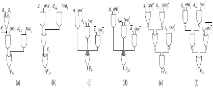
Fig.2.4. Generation of the ith Bit pj,i of PPj for a) Conventional, b) Pre-Encoded MB Multipliers, c) NR4SD-, d) NR4SD+ Pre-Encoded Multipliers, and e) NR4SD-, f) NR4SD+ Pre-Encoded Multipliers after reconstruction.
P a g e | 1463
Fig. 2.5. The ROM of pre-encoded multiplier with standard coefficients in MB Form.
2.2.3 Pre-Encoded NR4SD Multipliers Design:
The system architecture for the pre-encoded NR4SD multipliers is presented in Fig. 2.6. Two bits are now stored in ROM: n-2j+1, n+2j (Table 2) for the NR4SD or n+2j+1, n-2j (Table 2.3) for the NR4SD+ form. In this way, we reduce the memory requirement to n + 1 bits per coefficient while the corresponding memory required for the pre-encoded MB scheme is 3n/2 bits per coefficient. Thus, the amount of stored bits is equal to that of the conventional MB design, except for the most significant digit that needs an extra bit as it is MB encoded. Compared to the pre encoded MB multiplier, where the MB encoding blocks are omitted, the pre-encoded NR4SD multipliers need extra hardware to generate the signals of (6) and (8) for the NR4SD and NR4SDþ form, respectively. The NR4SD encoding blocks of Fig. 2.6 implement the circuitry of Fig. 2.7.
Fig. 2.6. System architecture of the NR4SD multipliers.
Each partial product of the pre-encoded NR4SD- and NR4SD+multipliers is implemented based on Figs. 2.4c and 4d, respectively, except for the PPk-1 that corresponds to the most significant digit. As this digit is in MB form, we use the PPG of Fig. 2.4b applying the change mentioned in Section 2.4.2 for the sj bit. The partial products, properly weighted, and the COR of (11) are fed into a CSA tree. The input carry cin,j of (11) is calculated as cin,j = two-j Vone-j and cin,j = one-j for the NR4SD- and NR4SD+ pre-encoded multipliers, respectively, based on Tables 2.2 and and 2.3. The carry-save output of the CSA tree is finally summed using a fast CLA adder.
3 REVIEWS OF BOOTH ENCODING AND RB PARTIAL PRODUCT GENERATOR
3.1 Radix-4 Booth Encoding
Booth encoding has been proposed to facilitate the multiplication of two‘s complement binary numbers. It was revised as modified Booth encoding or radix-4 Booth encoding. The MBE scheme is summarized in Table 1, where A =aN-1aN-2 ... a2 a1a0 stands for the multiplicand, and B= bN-1bN-2 ... b2 b1b0 stands for the multiplier. The multiplier bits are grouped in sets of three adjacent bits. The two side bits are overlapped with neighboring groups except the first multiplier bits group in which it is {b1, b0, 0}. Each group is decoded by selecting the partial product shown in Table 1, where 2A indicates twice the multiplicand, which can be obtained by left shifting. Negation operation is achieved by inverting each bit of A and adding ‗1‘ (defined as correction bit) to the LSB.Methods have been proposed to solve the problem of correction bits for NB radix-4 Booth encoding (NBBE-2) multipliers. However, this problem has not been solved for RB MBE multipliers.
TABLE 3.1 MBE Scheme
3.2 RB Partial Product Generator
As two bits are used to represent one RB digit, then a RBPP is generated from two NB partial products. The addition of two N-bit NB partial products X and Y using two‘s complement representation can be expressed as follows:
(2)
where is the inverse of Y , and the same convention is used in the rest of the paper. The composite number X; Y can be interpreted as a RB number. The RBPP is generated by inverting one of the two NB partial products and adding 1 to the LSB. Each RB digit Xi belongs to the set {1,0,1}; this is coded by two bits as the pair ðX i ; Xþ i Þ. Note that 1 ¼ 1. RB numbers can be coded in several ways. Table 2 shows one specific RB encoding [6], where the RB digit is obtained by performing Xþ i X i .
TABLE 3. 2 RB Encoding Used in This Work [6]
P a g e | 1465
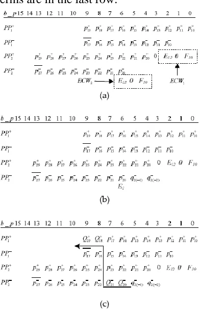
to the LSB of the partial product. A single ECW can compensate errors from both the RB encoding and the radix-4 Booth recoding. The conventional partial product architecture of an 8-bit MBE multiplier is shown in Fig. 3.1.
Fig. 3.1. Conventional RBPP architecture for an 8-bit MBE multiplier.
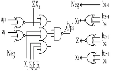
Where b_p represents the bit position, pþ ij or p ij is generated by using an encoder and decoder (Fig. 2).
Fig. 3.2. An encoder and decoder of the MBE scheme [10].
An N-bit CRBBE-2 multiplier includes N=4 RBPP rows and one ECW; the ECW takes the form as follows:
(3)
Where i represents the ith row of the RBPPs, Ei2 2 f g 0; 1 and Fi0 2 f g 0; 1 . In Fi0, a 1 correction term is always required by RB coding. If Fi0 also corrects the errors from the MBE recoding, then the correction term cancels out to 0. That is to say that if the multiplicand digit is inverted and added to 1, then Fi0 is 0, otherwise Fi0 is 1. The error-correcting digit Ei2 is determined only by the Booth encoding: E
(4)
As shown in Fig. 1 the first RBPP row, i.e. PP1, consists of the first partial product row PPþ 1 and the second partial product row PP 1 i.e., PP þ 1 ¼ pþ 19pþ 18 ... pþ 10and PP 1 ¼ p 17p 16 ... p 10, where, pþ 19 and pþ 18 are the sign extension bits, so pþ
(5)
(6)
According to Eq. (2), the sign extension bit pþ 29 is also the inverse of pþ 28. The p 17 in PP 1 and the p 27 in PP 2 are also negated as p 17 and p 27. Eq. (5) and Eq. (6) are further used in the next section when presenting the proposed modified RBPP generator.
For a 2n-bit CRBBE-2 multiplier, one additional RBPP accumulation stage is required due to the ECW. For a 64-bit RB multiplier, there are five RBPP accumulation stages; therefore, the number of RBPP accumulation stages can be reduced by 20 percent when eliminating the ECW in a 64-bit RB multiplier, which improves both the complexity and the critical path delay.
4. PROPOSED RB PARTIAL PRODUCT GENERATOR
4.1 Proposed RBMPPG2
Fig. 4.1 illustrates the proposed RBMPPG-2 scheme for an 88-bit multiplier. It is different from the scheme in Fig.4.1, where all the error-correcting terms are in the last row.
Fig. 4.1. (a) The first new RBMPPG-2 architecture for an 8-bit MBE multiplier; (b) the further revised RBMPPG-2 architecture by replacing E22 and F20 with E2, q 2ð2Þ, and q 2ð1Þ; (c) the final proposed RBMPPG-2 architecture by totally eliminating ECW2 and further combing E2 into Qþ 19, Qþ 18, Q 21, and Q 20.
ECW1 is generated by PP1 and expressed as
(7)
The ECW2 generated by PP2 (also defined as an extra ECW) is left as the last row and it is expressed as:
(8)
To eliminate a RBPP accumulation stage, ECW2 needs to be incorporated into PP1 and PP2. As discussed in Section 2.2 forFi0 and as per Table 1, F 20 is determined by b5; b4; b3 as follows:
(9)
As per Table 1, when b5b4b3 ¼ 111, 0 ¼ 0 can be used. Therefore, F20 can be expressed as follows:
(10)
By setting PPþ 2 to all ones and adding þ1 to the LSB of the partial product, F20 can then be determined only by b5 as follows:
(11)
P a g e | 1467
Fig.4.2. The modified radix-4 Booth encoding and decoding scheme for PP þ 2 .
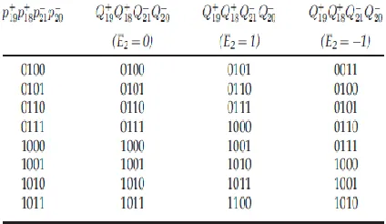
So, E22 and F20 in ECW2 are now determined by b7b6b5 without b4; b3. Although the complexity is slightly increased compared with the previous design (Fig. 2), the delay stage remains the same. In this work, Qþ 19, Qþ 18, Q 21, and Q 20 are used to represent the modified partial products (i.e., replacing pþ 19; pþ 18, p 21 and p 20). q 2ð2Þ, and q 2ð1Þ are used to represent the additional partial products that are determined by F20. As 1 can be coded as 111 in RB format, E22 and F20 can be represented by E2, q 2ð2Þ, q 2ð1Þ, (Fig. 3b) as follows:
(12)
(13)
As per Eq. (11) and Eq. (13), q 2ð2Þ, and q 2ð1Þ can also be expressed as follows:
(14)
This is further explained by the truth table of E22, F20 and E2, q 2ð2Þ, q 2ð1Þ (Table 3). Now ECW2 only includes E2 and E2 2 f g 0; 1; 1 ; E2 can be incorporated into the modified partial products Qþ 19, Qþ 18, Q 21 and Q 20 by replacing pþ 19, pþ 18 and p 21, p 20 in the shortest path Fig. 3c.
From the truth table, E2 can be determined by b7b6b5 as follows:
(15)
TABLE 4.1 Truth Table of E2, q 2ð2Þ, q 2ð1Þ and p 21, p 20 b7b6
So the following three cases can be distinguished: 1) When E2 ¼ 0, Qþ 19, Qþ 18, Q 21 and Q 20 remain unchanged as: Qþ 19 ¼ pþ 19, Qþ 18 ¼ pþ 18, Q 21 ¼ p 21 and Q 20 ¼ p 20. 2) When E2 ¼ 1, a 1 is added to pþ 19pþ 18p 21p 20. 3) When E2 ¼ 1, a 1 is subtracted from pþ 19pþ 18p 21p 20.
The relationships between Qþ 19, Qþ 18, Q 21, Q 20 and pþ 19, pþ 18, p 21, p 20 are summarized in Table 4.2. As the two MSBs of PP þ 1 i.e., pþ 19 and pþ 18 take complementary values as shown in Eq. (5), the operations of adding or subtracting a 1 will never incur in an overflow. Therefore, as per Eq. (15) and Table 4, the logic functions of Qþ 19, Qþ 18, Q 21, and Q 20 can be expressed as follows:
(16)
(17)
(18)
(19)
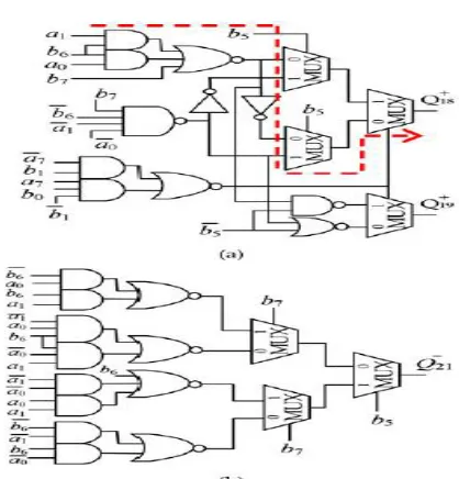
The delay of the RBMPPG-2 can be further reduced by generating Qþ 19, Qþ 18, Q 21, Q 20 directly from the multiplicand A and the multiplier B. The relationships between pþ 19, pþ 18 and A, B have been discussed in Section 2.2 as Eq. (5) and Eq. (6). The relationships
between p 21, p 20 and A, B are also shown in Table 3 according to the MBE scheme. Therefore, Qþ 19, Qþ 18, Q 21, and Q 20 can be expressed as follows by replacing pþ 19, pþ 18, p 21, and p 20 with the multiplicand bits (ai) and the multiplier bits (bi) after simplification:
(20)
(21)
(22)
(23)
P a g e | 1469
Fig. 4.3. The circuit diagram of the modified partial product variables: (a) Qþ 18 and Qþ 19, (b) Q 21.
The above discussion is only an example; the above technique can be applied to design any 2n-bit RB multipliers. It eliminates the extra ECWN/4 and saves one RBPP accumulation stage, i.e., three XOR gate delays, while only slightly increasing the delay of the partial product generation stage.
In general, an N-bit RB multiplier has N=4 RBPP rows using the proposed RBMPPG-2. The partial product variables pþ 1ðNþ1Þ, pþ 1N, p ðN=4Þ1 and p ðN=4Þ0 can be replaced by Qþ 1ðNþ1Þ, Qþ 1N, Q ðN=4Þ1, and Q ðN=4Þ0. The radix-4 Booth decoding of a PPR (PPþ N=4) needs additional three-input OR gates (Fig. 4). Therefore, the extra ECWN/4 is removed by the transformation of four partial product variables Qþ 1ðNþ1Þ, Qþ 1N , Q ðN=4Þ1, Q ðN=4Þ0 and one partial product row is saved in RB multipliers with any power-oftwo word-length.
4.2 Design of RBMPPG-2-Based High-Speed RB Multipliers
The proposed RBMPPG-2 can be applied to any 2n-bit RB multipliers with a reduction of a RBPP accumulation stage compared with conventional designs. Although the delay of RMPPG-2 increases by one-stage of TG delay, the delay of one RBPP accumulation stage is significantly larger than a one-stage TG delay. Therefore, the delay of the entire multiplier is reduced. The improved complexity, delay and power consumption are very attractive for the proposed design.
Fig. 4.4. The block diagram of a 32-bit RB multiplier using the proposed RBMPPG-2
The 64-bit RB-NB converter converts the final accumulation results into the NB representation, which uses a hybrid parallel-prefix/carry select adder (as one of the most efficient fast parallel adder designs). There are four stages in a conventional 32-bit RB MBE multiplier architecture; however, by using the proposed RBMPPG-2, the number of RBPP accumulation stages is reduced from 4 to 3 (i.e., a 25 percent reduction). These are significant savings in delay, area as well as power consumption. The improvements in delay, area and power consumption are further demonstrated in the next section by simulation.
TABLE 4.3 Comparisons of RBPP Accumulation Stages in RBPP Reduction Tree
Table 4.3 compares the number of RBPP accumulation stages in different 2n-bit RB multipliers, i.e., 8x8-bit, 16x16-bit, 32x32-bit, 64x64-bit multipliers. For a 64-bit multiplier, the proposed design has four RBPP accumulation stages; it reduces the partial product accumulation delay time by 20 percent compared with CRBBE-2 multipliers.
Although both the proposed design and RBBE-4 have the same number of RBPP
accumulation stages, RBBE-4 is more complex, because it uses radix-16 Booth encoding
.
III. RESULTS AND COMPARISION
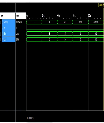
Fig. 4.5 Simulated output for Existing Pre-Encoded NR4SD Multipliers.
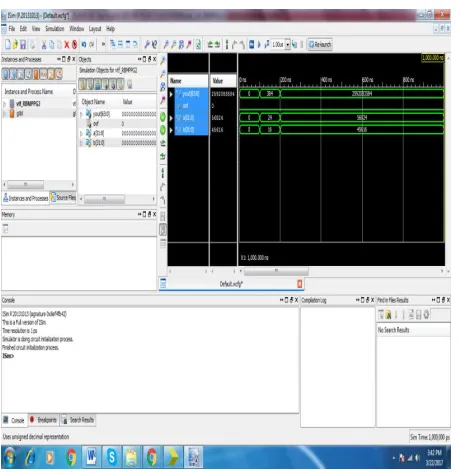
P a g e | 1471 Fig.4.6: Simulation of proposed 32x32 proposed
multiplier using RBMPPG
Table 4.4. Comparison Table for Area and delay of existing and proposed system:
S.no Description of Parameter
Existing System
Proposed System
1 Area 62% 54%
2 Delay 150.899 ns
115.791 ns
Compared to existing system the area and delays are less in proposed system. So, proposed system is preferable.
VI.CONCLUSIONS
A new modified RBPP generator has been proposed in this paper; this design eliminates the additional ECW that is introduced by previous designs. Therefore, a RBPP accumulation stage is saved due to the elimination of ECW. The new RB partial product generation technique can be applied to any 2n-bit RB multipliers to reduce the number of RBPP rows from N/4+1 to N/4.
Simulation results have shown that the performance of RB MBE multipliers using the proposed RBMPPG-2 is improved significantly in terms of delay and area. The proposed designs achieve significant reductions in area when the word length is at least 32 bits. Hence, the proposed RBPP generation method is a very useful technique when designing area of-two RB MBE multipliers. All the synthesis and simulation results of the proposed 32x32 multiplier using RBMPPG are performed on Xilinx ISE 14.7 using Verilog HDL
.
REFERENCES
[1] A. Avizienis, ―Signed-digit number representations for fast parallel arithmetic,‖ IRE Trans. Electron. Comput., vol. EC-10, pp. 389–400, 1961. [2] N. Takagi, H. Yasuura, and S. Yajima, ―High-speed VLSI multiplication algorithm with a redundant binary addition tree,‖ IEEE Trans. Comput., vol. C-34, no. 9, pp. 789–796, Sep. 1985. [3] Y. Harata, Y. Nakamura, H. Nagase, M. Takigawa, and N. Takagi, ―A high speed multiplier using a redundant binary adder tree,‖ IEEE J. Solid-State Circuits, vol. SC-22, no. 1, pp. 28–34, Feb. 1987. [4] H. Edamatsu, T. Taniguchi, T. Nishiyama, and S. Kuninobu, ―A 33 MFLOPS floating point processor using redundant binary representation,‖ in Proc. IEEE Int. Solid-State Circuits Conf., 1988, pp. 152–153.
[5] H. Makino, Y. Nakase, and H. Shinohara, ―A 8.8-ns 54x54-bit multiplier using new redundant binary architecture,‖ in Proc. Int. Conf. Comput. Des., 1993, pp. 202–205.
[7] Y. Kim, B. Song, J. Grosspietsch, and S. Gillig, ―A carry-free 54b54b multiplier using equivalent bit conversion algorithm,‖ IEEE J. Solid-State Circuits, vol. 36, no. 10, pp. 1538–1545, Oct. 2001.
[8] Y. He and C. Chang, ―A power-delay efficient hybrid lookahead carry-select based redundant binary to two‘s complement converter,‖ IEEE Trans. Circuits Syst. I, Reg. Papers, vol. 55, no. 1, pp. 336–346, Feb. 2008.
[9] G. Wang and M. Tull, ―A new redundant binary number to 2‘s-complement number converter,‖ in Proc. Region 5 Conf.: Annu. Tech. Leadership Workshop, 2004, pp. 141–143.
[10] W. Yeh and C. Jen, ―High-speed booth encoded parallel multiplier design,‖ IEEE Trans. Comput., vol. 49, no. 7, pp. 692–701, Jul. 2000.
[11] S. Kuang, J. Wang, and C. Guo, ―Modified Booth multiplier with a regular partial product array,‖ IEEE Trans. Circuits Syst. II, vol. 56, no. 5, pp. 404–408, May 2009.
[12] J. Kang and J. Gaudiot, ―A simple high-speed multiplier design,‖ IEEE Trans. Comput., vol. 55, no. 10, pp. 1253–1258, Oct. 2006.
![TABLE 3. 2 RB Encoding Used in This Work [6]](https://thumb-us.123doks.com/thumbv2/123dok_us/7747324.1269536/8.612.87.284.528.630/table-rb-encoding-used-work.webp)