Design and Implementation of CMOS
Frequency Synthesizer Using Phase Lock
Loop (PLL) with Low Power Consumption in
0.25 µm CMOS Technology
Ankita Choudhary 1, Rakesh Mandilya 2
M.Tech Scholar, Dept. of ECE, BMCT, Indore, India1
Asst. Professor, Dept. of ECE, BMCT, Indore, India 2
ABSTRACT:The needs for low power and high speed circuits are increasing in modern electronics. The carrier generation and phase locking are very important for transceiver circuits. The frequency synthesizer based on the phase-locked loop (PLL) is a basic building block of the transceiver. The frequency synthesizer that generates carrier for the down-conversion/up-conversion operations, it operates at high frequency and it consumes a very large portion of the total power of the circuit. The frequency synthesizer based on phase lock loop consists of voltage controlled oscillator, phase detector; low pass filter and N frequency divider. The voltage controlled oscillator (VCO) and N frequency divider consumes the maximum power. This paper presents a frequency synthesizer which is designed with low power consumptions voltage controlled oscillator (VCO) circuit and frequency divider circuit. Finally we proposed a phase lock loop N frequency synthesizer using the proposed low power building blocks and results of our low power PLL frequency synthesizer.
KEYWORDS: Frequency Synthesizer, PLL, VCO, and Charge Pump
I. INTRODUCTION
Phase lock loops are very essential part of the transceiver, they lock the phase of the feedback signal to the reference signal. phase lock loops (PLLs) are mixed signal building elements which are widely used in integrated circuits (IC) design [1]. The phase lock loop systems are widely used in many applications such as synchronization circuits carrier generation circuits, N-frequency synthesizers, phase modulation and demodulation, clock recovery and clock generation circuits. The phase lock loops are commonly embedded and they are used in highly integrated cellular RF CMOS circuits. Moreover, they are important block for embedded systems like wireless phones, micro-computers, chain transceiver of RF sensor and is even expected to appear soon on other purely digital circuits such as digital signal processing and field effect transistors gate arrays[2]. N-frequency divider Pump and Phase Frequency Detector circuits are essential building blocks of frequency synthesizers based on phase lock loops. This paper proposed a CMOS frequency synthesizer using phase lock loops with low power consumption for low power and low supply circuits using
0.25μm CMOS technology. The objective of this research paper is to design and implement the critical blocks such as
voltage controlled oscillator (VCO) and frequency divider which consume maximum power in the phase lock loop
systems. The proposed circuit has simple structure and implemented in 0.25 μm CMOS technology. It provides more
II. FUNDAMENTALS OF FREQUENCY SYNTHESIZERS BASED ON PLL
Fig 1.1 Basic phase lock loop
II. PROPOSED WORK
This section describes the proposed work. The main objective of this proposed work is to design and implement the critical blocks like phase and frequency detector (PFD) block and voltage controlled oscillator (VCO), charge pump and frequency divider for the frequency synthesizer with low power consumption. The performance in power consumption and channel selection of frequency synthesizer are limited by the two most important building blocks, namely the voltage-controlled oscillator (VCO) and the high frequency divider.The main idea of this proposed phase lock loop is that only voltage controlled oscillator (control voltage) or loop dynamic will controlled the switch control and hence no external control is required. The power consumption and channel selection of frequency synthesizer are limited by the two most important building blocks, namely the voltage-controlled oscillator (VCO) and the high frequency divider.
III. DESIGN METHODOLOGY
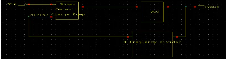
Fig.3.1 shows the schematic diagram of proposed frequency synthesizer using phase lock loop designed in tanner eda tool. The main components of frequency synthesize are phase detector, charge pump, voltage controlled oscillator and N frequency divider.In this work the components of frequency synthesizer are designed individually for low power consumption. After the PLL circuit analysis from the previous studies and documentation, it is implemented and simulated on Tanner tool. The results are extracted and recorded for the comparative study of PLL. Vin is referred as input frequency and the output frequency is obtained from the Voutport of the proposed circuit shown in fig.3.1.
1. PLL Design and Simulation
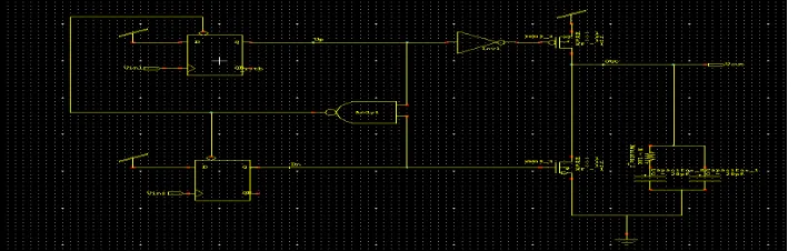
The first block of PLL is phase and frequency detector (PFD) shown in fig. 3.2 is designed and implemented and then it is simulated in tanner tool. The simulation experiment results are shown in fig. 3.3. In this unit, The blocks like phase and frequency detector (PFD), Charge Pump (CP) and Low pass loop filter are implemented as shown in fig. 3.2. The first block phase and frequency detector (PFD) consists of two D flip flops and a NAND gate the output NAND gate is connected to the reset of the both D-flip flop. Charge Pump is made NMOS (NMOS_3) and PMOS (PMOS_3) transistor connected in series. The output of one of the D-flip flop is feed to PMOS_3 through inverter. NMOS_3 transistor is connected directly to another D-flip flop. This charge pump circuit acts as an inverter and is used to combine both the output of phase and frequency detector (PFD)
Fig 3.2 Schematic diagram of PFD, Charge pump and Filter
and give a single output which is fed to the input of the filter. The filter consists of two capacitor of same values and a resistor. The proposed designed is simulated in the tanner tools and the experimental results of schematic is observed on the W (waveform)-edit of the Tanner tool. The output voltage as the transient response gives oscillations as shown in fig. 3.3. The charge pump current is also calculated through this corresponding waveform. The fig. 3.3 shows the oscillation waveform of phase lock loop (PFD).
.
Fig. 3.3 Transient response of PFD.2. Voltage controlled oscillator (VCO) Design and Simulation
Fig. 3.4 shows the ring VCO. The schematic of ring oscillator consists of four inverters connected back to back. The experimental result of voltage controlled oscillator is observed are shown in fig.3.4.
The output voltage as the transient response provides oscillations. This output voltage will appear which will give the measure of frequency. The frequency for the time instants can be calculated through this corresponding voltage.
3. N-FREQUENCY DIVIDER DESIGN AND SIMULATION
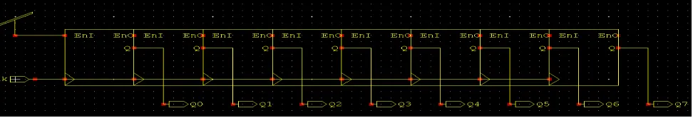
The N-frequency divider acts as a feedback loop for the frequency synthesizer using phase lock loop. This circuit is implemented using 8-bit counter and there are eight T-flip flop are used in serially back to back to implement the 8-bit counter is shown in fig. 3.5.
Fig. 3.5 8 bit counter using T-flip flop
The simulation results of 8 bit counter is shown in fig. 3.6. The figure shows the transient response of the 8 bit counter.
Fig. 3.6 Simulation waveform of counter
4. PROPOSED FREQUENCY SYNTHESIZER USING PLL DESIGN AND SIMULATION
The individual components are discussed above are connected in a signal circuit to form phase lock loop circuit. As it is earlier described that the integer n frequency synthesizer using Phase Lock Loop here made by using Phase frequency detector (PFD) ,Charge pump (CP) ,Loop Filter, ring voltage controlled oscillator (VCO) and an 8-bit counter (acts as a feedback loop) is.
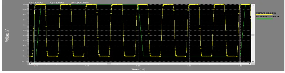
The simulated experimental results of proposed frequency synthesizer is observed and analyzed. The final output waveform of Frequency Synthesizer using Phase Lock Loop (PLL) is shown in fig 3.7.
IV. SIMULATION RESULTS
The simulation results are discussed in this section, the parameters such as power consumption and its output frequency of frequency synthesizer. The key parameter of the circuit is power consumption. The total power consumed by the integral parts of the circuit such as VCO, (PFD), Charge pump and frequency divider.
Fig 4.1 Output frequency of frequency synthesizer
The proposed design is implemented and simulated in tanner EDA tool with the supply voltage of 1V. The average power is calculated by averaging. The power consumed by the proposed frequency synthesizer is calculated. The maximum power (Pmax) consumed by the circuit is 2.237963 mW at time 2.20726µs and the minimum power Pmin is
observed at time 6.517µs is 1.027692 nW at supply voltage 1 Volt. Therefore the average power of the circuit gives the total power consumed by the circuit. The average power of the circuit is calculated as 0.1873 mW. The frequency of the proposed frequency synthesizer is calculated from the output waveform of the proposed frequency synthesizer as shown in fig. 4.1. The range of output frequency of proposed frequency synthesizer is 100MHz to 200MHz.
V.COMPARATIVEPERFORMANCE
S.No Parameters [10] [12] My Work
1. Tool Tanner Tool
2. Technology 240nm 250nm 250nm
3. Power supply (Vdd) 2.5 V 2.5v 1V
4. Reference Frequency 20MHz-2GHz 70MHz 5MHz
5. Gate length 0.24µm 0.25µm 0.25µm
6. Output Frequency 350MHz-1.25GHz 180-320MHz 100-200MHz 7. Power Consumption <300mW 3.875mW 0.1873 mW
VI. CONCLUSION
lock loop (PLL). The main idea of this proposed work is that the switch control will be controlled only by the voltage controlled oscillator (VCO) therefore there is no need of control externally that consumes extra power. The objective of this proposed work is to design the critical blocks for the frequency synthesizer with low power consumption. The power consumed by the circuit is calculated as 0.1873mW and this proposed circuit can operate from 100MHz to 200MHz.
REFERENCES
[1] Neil H.E.Weste and David Money Harris “CMOS VLSI – A Circuits and Systems Perspective Fourth edition”
[2] R.J.Baker, H.W.Li, and D.E.Boyce, “CMOS Circuit Design, Layout, and Simulation,” IEEE Press Series on Microelectronic Systems, 2002. [3] Gayathri M G* “Design of All Digital Phase Locked Loop in VHDL” Gayathri M G / International Journal of Engineering Research and Applications (IJERA) ISSN: 2248-9622 www.ijera.com Vol. 3, Issue 4, Jul-Aug 2013, pp.1074-1076
[4] W. Alan Davis, Krishna Agarwal “Radio Frequency Circuit Design” Copyright 2001 John Wiley & Sons, Inc. Print ISBN 0-471-35052-4 Electronic ISBN 0-471-20068-9
[5] General PLL Description: T. H. Lee, Chap. 15. Gray and Meyer, 10.4 Clock generation: B. Razavi, Design of Analog CMOS Integrated Circuits, Chap. 15, McGraw-Hill, 2001.
[6] VemulaLohith Kumar1 1BTech Student, School of Electronics, Vignan University, Vadlamudi, Guntur, AP, India ‘Simulation of Integer N Frequency Synthesizer’ International Journal of Engineering Trends and Technology (IJETT) - Volume4 Issue6- June 2013
[7]Kanika Garg, ACSD Department, CDAC1; V.SulochanaVerma, ACSD Department, CDAC2 “DESIGN OF LOW POWER PHASE LOCKED LOOP IN SUBMICRON TECHNOLOGY” International Journal of Advanced Technology & Engineering Research (IJATER)
[8] Yashpal Sen1 and Nitin Jain2 1M.Tech. Scholar, Dept. of ET&T (Digital Electronics) C.E.C., Bilaspur, CSVTU, (C.G.), INDIA. 2Dept of E&TC, C.E.C., Bilaspur, CSVTU, (C.G.), INDIA. “Design and Implementation of Phase Locked Loop Using Current Starved Voltage Controlled Oscillator” Advance in Electronic and Electric Engineering. ISSN 2231-1297, Volume 4, Number 6 (2014), pp. 637-644 © Research India Publications
[9] K.Rajasekhar, S.Adilakshmi, T.B.K. Manojkumar “Design of High Performance Phase Locked loop for Multiple outputs with Ultra Low Power Sub Threshold Logic” International Journal of Engineering Research and Applications (IJERA) ISSN: 2248-9622 www.ijera.com Vol. 2, Issue 2,Mar-Apr 2012, pp.046-052
[10] A FULLY INTEGRATED CMOS PHASE-LOCKED LOOP WITH 30MHZ TO 2GHZ LOCKING RANGE AND ±35PS JITTER BY Chao Xu, Winslow Sargeant, Kenneth R. Laker, Jan Van der Spiegel Paper published in Journal of Analog Integrated Circuits and Signal Processing", July-August 2003, Volume 36,
[11] Dr.P.H.Tandel, Anuradha P. Gharge “Design of General Order Digital Phase Locked Loop” International Journal of Engineering and Innovative Technology (IJEIT) Volume 2, Issue 7, January 2013
[12] AnithaBabu, BhavyaDaya, BanuNagasundaram, NivethaVeluchamy “All Digital Phase Locked Loop Design and Implementation” University of Florida, Gainesville, FL, 32608, USA
[13] Varsha Prasad 1, Dr Chirag Sharma 2 “A Review of Phase Locked Loop” International Journal of Emerging Technology and Advanced Engineering Website: www.ijetae.com (ISSN 2250-2459, Volume 2, Issue 6, June 2012)
[14] Guan- Chyun Hsieh, senior member,IEEE, and James C.Hung,Fellow,IEEE “Phase- Locked Loop Techniques- A Survey” IEEE TRANSACTIONS ON INDUSTRIAL ELECTRONICS, VOL.43,NO.6,DECEMBER 1996
[15] Curtis Barret “Fractional/Integer-N PLL Basics” Technical Brief SWRA029
[16] Tianwang Li, Bo Ye and Jinguang Jiang,” 0.5 V 1.3 GHz voltage controlled ring oscillator” 2009 IEEE [17] B .Razvi, “Design of ANALOG CMOS Integrated Circuits” McGraw- Hill, 2001.
[18] K. Shu, E. Sanchez-Sinencio, J. Silva-Martinez, and S.H.K. Embabi, “A 2.4-GHz monolithic fractional-N frequency synthesizer with robust phase-switching prescaler and loop capacitance multiplier”, IEEE Journal of Solid-State Circuits, vol. 38, no. 6, pp. 866-874, June 2003.
[19] VolodymyrKratyuk, Pavan Kumar Hanumolu, Un-Ku Moon,andKartikeyaMayaram, “A Design Procedure for All-Digital Phase-Locked Loops Based on a Charge-Pump Phase-Locked-Loop Analogy” IEEE TRANSACTIONS ON CIRCUITS AND SYSTEMS—II: EXPRESS BRIEFS, VOL. 54, NO. 3, MARCH 2007
[20] KusumLata and Manoj Kumar “ALL Digital Phase-Locked Loop (ADPLL): A Survey” International Journal of Future Computer and Communication, Vol. 2, No. 6, December 2013
[21] Abhilasha N.S “Optimized Design of Digital Phase Locked Loops for RF Carrier Acquisition” IJESRT (INTERNATIONAL JOURNAL OF
ENGINEERING SCIENCES & RESEARCH TECHNOLOGY) ISSN: 2277-9655
Scientific Journal Impact Factor: 3.449 (ISRA), Impact Factor: 1.852 ,May 2014
[23] Kilian Imfeld “Low-Jitter and Low-Power CMOS PLL for Clock Multiplication”, Solid-State Circuits Conference, 2006. ESSCIRC 2006, pp-174-177.
[241] H.-T.Ahm and D.J.Allstot,”A low-jitter 1.9-V CMOS PLL for ultraSPARC microprocessor applications,”IEEEJ.Solid-States Circuits, vol.35,pp.450-454,May 1999.
[25] I.Hwang, S.Lee, S.Lee and S.Kim,”A digitally controlled phase locked loop with fast locking scheme for clock synthesis applications,”in IEEE Int.Solid-State circuits Conf.Dig.Tech.Papers, Feb.2000, pp.168-169.