Design of Low Power Counters Using
Reversible Logic
Asima Jamal1, Jai Prakash Prasad2
P.G. Student, Department of ECE, Don Bosco Institute of Technology, Bangalore, Karnataka, India1
Associate Professor, Department of ECE, Don Bosco Institute of Technology, Bangalore, Karnataka, India2
ABSTRACT: In today’s world, the complexity of the chip is increasing as more and more devices are being connected on a single chip. Due to the high density of the chip, the power dissipation increases demanding better power optimization methods. One of the methods to achieve power optimization is by using reversible logic. It can be used in low power CMOS designs, quantum computing, nanotechnology and optical computing.
This paper presents an optimized sixteen-bit binary sequential counter based on reversible logic using Feynman, and Fredkin gates. Optimization of the sequential circuit is achieved on the basis of total number of gates used in the circuit and total number of garbage outputs generated. Circuits have been designed using Cadence Virtuoso Schematic Editor.
KEYWORDS:Reversible Logic, Circuit Designing using Reversible Gates, Reversible Logic Gates, Binary Counter.
I. INTRODUCTION
The typical computer is logically irreversible - its transition function i.e., the partial function that maps each whole-machine state onto its successor, if the state has a successor, lacks a single-valued inverse which means models of computation which are logically irreversible lose information in the process of execution, that lost information is actually translated in the form of heat. So loss of information results in power dissipation.
Landauer has shown that for irreversible logic computations, each bit of information which is erased or thrown away, produces kTln2 joules of heat energy, where k is Boltzmann’s constant and T the absolute temperature at which computation is represented [1]. Bennett demonstrated that kTln2 energy dissipation can be reduced, if a computation is carried out in a reversible way [2], since the amount of energy dissipated in a system bears a direct relationship to the number of bits erased during computation.
For room temperature T, the amount of heat dissipated for one bit is small i.e. 2.9×10⁻²¹ J [3]. This heat dissipation extremely reduces the performance and lifetime of the circuits. The solution is to use revolutionary technology which enables extremely low power consumption and heat waste in computing [4]. It made clear that, for reducing the power dissipation in the arbitrary circuit, it must be built from reversible gates. Reversible circuits are of particular interest in low power CMOS VLSI design.
In 1965 Gordon Moore observed that the performance of integrated circuit would continue to improve at an exponential rate with the performance per unit cost increasing by a factor of 2, every 18 months.
According to Gordon Moore [3], shrinking the dimensions on integrated structures makes it possible to
operate the structure at a higher speed for the same power per unit area. As more and more components are getting packed onto the chip, power dissipation in the present day computer is becoming very high. Perkowski et.al.’s states [4] “every future technology will have to use reversible gates in order to reduce power” This has led many people to pursue research in the area of reversible logic.
According to Frank [5], computers based mainly on reversible logic operations can reuse a fraction of the signal energy that theoretically can approach arbitrarily near to 100% as the quality of the hardware is improved.
Reversible circuits do not lose information and reversible computation in a system can be performed only when the system consists of reversible gates. Reversible logic is likely to be in demand in high speed power aware circuits, low power CMOS design. The main challenges of designing reversible circuits are to reduce number of gates, garbage outputs, delay and quantum cost. Another important matter is hardware complexity.
Reversible logic supports the process of running the system both forward and backward. This means that reversible computations can generate inputs from outputs and can stop and go back to any point in the computation history.
II. LITERATURE SURVEY
Landauer [1] has shown that for every bit of information lost in logic computations that are not reversible, KT ln2 joules of heat energy is generated, where k is Boltzmann’s constant and T the absolute temperature at which computation is performed. The amount of energy dissipation in a system increases in direct proportion to the number of bits that are erased during computation.
Bennett [2] showed that KT ln2 energy dissipation would not occur, if a computation were carried out in a reversible way. Thus, a reversible operation ensures low energy dissipation. Since the energy dissipated in CMOS cells is proportional to the number of transitions, to the output load, and to the square of the operating voltage. Energy of E= ½CV2 is stored and this energy gets dissipated whenever switching occurs in conventional (irreversible) logic implemented in modern CMOS technology, we reduce the number of transitions, the capacitance, and the voltage [9]. There are a variety of considerations that must be taken into account in low-power design which include the style of logic, the technology used, and the logic implemented. Factors that were shown to contribute to power dissipation included spurious transitions due to hazards and critical race conditions, leakage and direct path currents, pre-charge transitions, and power-consuming transitions in unused circuitry.
III. PROBLEM FORMULATION
According to Landauer, computing machines inevitably involve devices which perform logical functions that have a
single valued inverse
. T
he energy consumption in computer is due to logically irreversible operation where theinformation is erased or thrown away. For example, the commonly used AND gate, which has two input and one output, one bit is lost when the information goes through this gate, this loss is in the form of heat. About kT*ln 2 joules of energy is generated for every bit of information which is lost. In the design of integrated circuits many technologies like lower work voltage, putting the management of power supply and lowering the channel length of MOSFETS have been applied. However, the power dissipation is reduced in logical operations. But in future, where the size of MOSFETs is shrinking, we need to find the alternative method for lowering the power dissipation that will encounter the barrier of kT. There are two effective ways to overcome this problem, one is reducing the temperature of the computer and the other is by constructing the reversible computer on thermodynamics. According to the theory and analysis of Frank, when the temperature is reduced to 0 K, the power dissipation reduces two orders of magnitude but practically this cannot be maintained constant. Later Bennett showed that reversible logic can be used to reduce the power dissipation. The key point of reversible computing is that the electric charge on the storage cell consisting of transistors is not permitted to flow away when the transistor is switched. Then it can be reused through reversible computing, which can decrease the energy consumption. When there is no loss of information bits, then the system is reversible.
IV. REVERSIBLE LOGIC
Reversible computing was started when the basis of thermodynamics of information processing was shown that conventional irreversible circuits unavoidably generate heat because of losses of information during the computation.
positive to negative: bits from zero to one. Most of the energy needed to make that change is given off in the form of heat. Rather than changing voltages to new levels, reversible circuit elements will gradually move charge from one node to the next. This way, one can only expect to lose a minute amount of energy on each transition. Reversible computing strongly affects digital logic designs. Reversible logic elements are needed to recover the state of inputs from the outputs. It will impact instruction sets and high-level programming languages as well. Eventually, these will also have to be reversible to provide optimal efficiency.
Reversible computing provide reliable and low power design, high performance circuits synchronous with speed and processing power. It improves computational efficiency and this can be done by building circuits which reduce energy from state will save energy. Reversible computing will also lead to improvement in energy efficiency. It increases portability of device to reduce element size to atomic size. It incur more hardware cost, but power cost and performance are dominant than hardware cost. Hence need of reversible computing cannot be ignored in computing era. Some factor regarding reversible logic are given below
The number of garbage outputs (GO): This refers to the number of unused outputs present in a reversible logic
circuit. These garbage outputs cannot be neglected as these are very essential to achieve reversibility. These should be minimum.
Quantum cost (QC): This refers to the cost of the circuit in terms of the cost of a primitive gate. It is calculated
by knowing the number of primitive reversible logic gates (1 * 1 or 2*2) required to realize the reversible circuit.
The number of constant inputs (CI): This refers to the number of inputs that are to be maintained constant at
either 0 or 1 in order to synthesize the given logical function. Number of constants should be minimum
MOSFETS (transistors): This refers to the number of MOSFET used to construct the entire design. It’s better
to use minimum number for MOSFETS.
Total power (TP): This refers to the total power dissipated during logical operation in entire design by using
CMOS logic.
Delay (D): Maximum number of unit delay gates in the path of propagation of inputs to outputs. It represents
number of reversible gates used between the primary inputs and the outputs of a reversible logic circuit.
V. REVERSIBLE LOGIC GATES
A logic gate L is said to be reversible if, for any output y, there is a unique input x such that applying L(x) = y. If a
gate L is reversible, there is an inverse gate L′ which maps y to xfor which L′(y) = x. A reversible logic gate has equal
number of input and output terminals and there is one to one mapping between them. A gate is called reversible because both forward and backward computation can be performed. Reversible gate should practically loose very little amount of energy. Fan-out is not allowed in reversible circuits however fan-out can be achieved using additional gate. In this project, basic reversible gate like Feynman gate and Fredkin gate are used for implementing TFF gate and reversible sequential circuits.
A. FEYNMAN GATE
Feynman gate is a 2*2 one through reversible gate as shown in figure l. It is also called as controlled NOT gate (CNOT). The input vector is I (A, B) and the output vector is O (P, Q). Feynman Gate (FG) can be used as a copying
gate. Since a fan-out is not allowed in reversible logic, this gate is useful for duplication of the required outputs.
Figure 1: Feynman Gate Figure 2: Quantum implementation of Feynman Gate
Figure2 shows the quantum implementation of Feynman gate. The outputs are defined by P=A, Q=A⊕B. Quantum
Figure 3: Transistor implementation of Feynman Gate
Figure 3 shows the transistor implementation of the Feynman gate. The transistor implementation is fully reversible, that is, the given circuit can also work for forward as well as reverse operation.
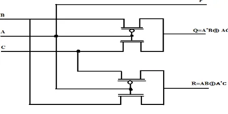
B. FREDKlN GATE
Figure 4 shows a 3*3 Fredkin gate. The Fredkin gate is a reversible 3-bit gate that swaps the last two bits if the first
bit is 1, i.e., a controlled-swap operation
.
It is used as a 2:1 mux and out of three inputs, one input acts as enable. Theinput vector is I (A, B, C) and the output vector is 0 (P, Q, R). The output is defined by P=A, Q=A'B ⊕ AC and
R=A'C ⊕ AB. Quantum cost of a Fredkin gate is 5.
Figure 4: Fredkin Gate Figure 5: Quantum implementation of Fredkin Gate
Figure5 shows the quantum implementation of Fredkin gate. The output is defined by P=A, Q=A'B ⊕ AC and
R=A'C ⊕ AB. Quantum cost of a Fredkin gate is 5. It is also a one through gate since one of its input is the output.
Figure 6: Transistor implementationof Fredkin Gate
VI. FLIP FLOP IMPLEMENTATION
A. T FF Implementation Using Reversible Gates
Figure 7: TFF Implementation using Fredkin and Feynman gate (positive level triggered)
The TFF is designed using the basic gates such as Fredkin and Feynman gates so as to implement the design with minimum transistors. The design is shown in Figure 7 as above.
A Fredkin gate is used as a 2:1 mux and the Feynman gate is used for getting fan-out of 2. The XOR functionality is added by a single Feynman gate.
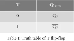
Table I: Truth table of T flip-flop
As shown in Table I, when T = 0, the flip flop does a hold. A hold means that the output, Q is kept the same as it was before the clock edge. When T = 1, the flip flop does a toggle, which means the output Q is negated after the clock edge, compared to the value before the clock edge.
VII. COUNTER IMPLEMENTATION
Sixteen Bit Asynchronous Reversible Up/Down Counter
The implementation of reversible asynchronous & synchronous Up/Down Counter is shown in Fig. 13 [6]. The Up/Down operation of this reversible circuits is controlled by the control input UP/DOWN. For UP operation, the control input should be 1 and for down operation, the control input should be 0.
Figure 8: Sixteen-bit Asynchronous Reversible Up/Down
VIII. SIMULATION RESULTS
Proposed circuits have been implemented and simulated using Cadence virtuoso tool.
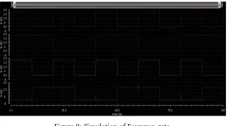
A. FEYNMAN GATE
Figure 9: Simulation of Feynman gate
Figure 9 shows the simulation result of Feynman gate. When A=0, Q=B and when A=1, Q=B
'.
B. FREDKIN GATE
Figure 10: Simulation of Fredkin gate
Figure 10 shows the simulation result of Fredkin gate. When A=0, Q=B, R=C and when A=1, Q=C, R=B
.
C. T FLIP FLOP
Figure 11 : Simulation of T Flip flop
Figure 11 shows the simulation result of T Flip-flop. When T input is high, output will changes its state during the
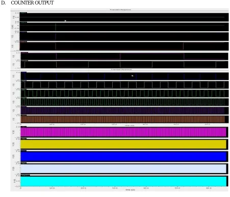
D. COUNTER OUTPUT
Figure 12: Simulation of counter
Figure 12 shows the simulation result of a 16-bit counter. It counts from 0 to 216.
IX. APPLICATION
X. CONCLUSION
This paper proposes design of sixteen bit asynchronous and synchronous up/down counter using both irreversible & reversible logic. It is observed that reversible circuits will have less power consumption compared to irreversible circuits. Basic reversible gate presented in this project can be used in regular circuits realizing Boolean functions. The proposed synchronous counter designs have the applications in building reversible ALU, reversible processor etc. In this project, a method of asynchronous & synchronous counter design directly from reversible gates is presented. This work forms an important move in building large and complex reversible sequential circuits so as to reduce the power consumption and improve application in low power and nano-technology.
REFERENCES
[1] Landauer, R., "Irreversibility and heat generation in the computing process", IBM 1. Research and Development, 5(3): pp. 183-191, 1961. [2] Bennett, C.H., "Logical reversibility of Computation", IBM J.Research and Development, 17: pp. 525-532, 1973.
[3] M.P.Frank, Introduction to reversible computing: motivation, progress ,and challenges. In Proceedings of the 2nd Conference on Computing Frontiers, pages 385–390, 2005.
[4] Toffoli. T. “Reversible Computing,” Tech memo MIT/LCS/TM-151, MIT Lab for Comp. Sci., 1980.
[5] V.Rajmohan, V.Ranganathan,"Design of counter using reversible logic" 978-1-4244-8679-3/11/$26.00 ©2011 IEEE
[6] Siva Kumar Sastry, Hari Shyam Shroff ,Sk.Noor Mahammad, V. Kamakoti" Efficient Building Blocks for Reversible Sequential Circuit Design" 1-4244-01739106/$20.00©2006IEEE
[10] M.-L. Chuang and c.-Y. Wang, "Synthesis of reversible sequential elements," ACM journal of Engineering Technologies in Computing Systems (JETC), vol. 3, no. 4, 2008.
[7] S.K.S. Hari, S. Shroff, S.N. Mohammad, and V. Kamakoti, "Efficient building blocks for reversible sequential circuit design," IEEE International Midwest Symposium on Circuits and Systems (MWSCAS), 2006.
[8]Abu Sadat Md. Sayem, Masashi Veda "Optimization of reversible sequential circuits" journal of computing, volume 2, issue 6, issn 2151-9617, june 2010.