warwick.ac.uk/lib-publications
A Thesis Submitted for the Degree of PhD at the University of Warwick
Permanent WRAP URL:
http://wrap.warwick.ac.uk/97339
Copyright and reuse:
This thesis is made available online and is protected by original copyright.
Please scroll down to view the document itself.
Please refer to the repository record for this item for information to help you to cite it.
Our policy information is available from the repository home page.
I
Attention is drawn to the fact that the
copyright o f this thesis rests with its author.
This copy o f the thesis has been supplied
on condition that anyone who consults it is
understood to recognise that its copyright rests
with its author and that no quotation from
the thesis and no information derived from it
may be published without the author’s prior
written consent.
T) lS 3 f f | 7 7
v o i r
for the
Computer Aided
Design
of
L in e a r M icro w ave C ircu its
A uthor
B rian G. M a rch e n t, B. Sc. (Hons.)
A thesis submitted at the University of Warwick for the degree of Doctor of
and almost any microwave circuit could be handled by the method
of analysis used in this program.
During the development of the programs, as each new program
was developed, more facilities were included for the interactive on-line use of the programs. In the KICK03 program a list
processing approach to the data structure in the program and a full syntactical analysis of the data was included. This made
it possible to generate very complex data structures in the program thus making the program ideal for interactive on-line use on a computer. The data for this program was more like a
programming language than normal data and any data error could be correct on-line during the run of the program. The program
could be used on batch processing, on a remote teletype interactively or with a graphical display to display the results of an analysis
in graphical form.
The idea for the research work cont led in this Ph. D. thesis originated from a suggestion to the author by Mr. M.K. licPhun at the University of WarwicK in November 1968 that research work
in the field of the Computer Aided Design of Microwave Circuits would bo a very uceful research topic for a Ph. D. thesis. The
research work on this topic started in ¡lay
1969
when the author started working with Microwave Associated Ltd., Luton whilst waiting for a Science Research Council grant to Gtart in October1969
. Then a move was made to the School of Engineering Science at the University of Warwick where the main part of the research work was carried out up to October 1972. Also in February 1970 the Science Research Council grant was changed to an industrial studentship grant between the Science Research Council and RedacSoftware Ltd.. The writing of this thesis was completed in the author's spare time whilst working with Redac Software Ltd.,
Tewkesbury after October 1972.
At Microwave Associates Ltd., Luton experience was obtained in the ‘heorectical design of microwave integrated circuits.
To assist with this work a remote teletype terminal for a time sharing computer was used at LuLon for microwave circuit synthesis whilst the computer program written by M c P h u n ”* ^ using chain matrix analysis was used for circuit analysis on the Elliott U
13
O computer at the University of Warwick. Two prob]«mo were investigatedsecond problem it was found that McPhun'c computer (
0
.1
)program was not suitable for the types of circuits to be analysed. Thus a new computer program, BGMA^'"^, had to be written by the author for this work to extend the ideas contained in KcPhun's program.
On arriving at the University of Warwick in October 1969 a year was spent almost entirely on extending the appication of the chain matrix method of analysis for the analysis of general
microwave circuits. During this period the CHAIN1 program^
was written by the author using chain matrix analysis for the analysis of general microwave circuits. This program analysed a
circuit consisting of an assembly of 2-port networks and it broke this assembly down into a simpler assembly of cascades of 2-port networks forming a nain link between the input and output port of the circuit and branch arms, loop paths and parallel paths built to any level on this main path.
Towards the completion of the work on developing the CHAIN1 program it was realised that the use of the chain matrix method
of analysis had been taken just about to its limit but it could still not analyse all microwave circuits. Also at that time the use of the chain matrix method of analysis for general microwave circuits was being critised by Dr. Lurcombe, University of Warwick
and Mr. Wolfendale, Redac Software Ltd.. Thus at that time it became necessary to completely rethink the method of analysis being used. The result of this was that it was decided to use a previously untried method for the analysis of microwave circuits.
The new method used was the mixed matrix method of
analysis for general microwave circuits considered as an assembly
(
0
.
6
)
0.3
-suitable. The MICRO2 computer p r o g r a m ^ ’^ 1 was written by the author
to use this method of analysis. This program took about a year to write and was later replaced by the MICR03 computer program
which incorporated more facilities ( see Appendix A.5 )•
During the course of the research work for this thesis there was a considerable amount of interest shown by the University of Warwick in the use of computer programs in an interactive mode.
Thus a large portion of the time spent in writing the BGMA, CHAIN"), MICR02 and KICR03 programs was spent on developing interactive applications for these programs with each program including more interactive facilities than the last one. This work involved developing techniques for a full syntax analysis of the data,
the use of complex,but very versatile,data structures and the use of the program interactively on a remote teletype possibly with a graphical display to display the results of a circuit analysis in graphical form. The result was that in the MICR03 program all these facilities were included and the data for the program had more the form of a compul.-r programming language that the normal
data for a program.
Some time was spent during the course of the research for this thesis investigating the range of microwave components which should be included in a computer program for the analysis of microwave circuits. Also an investigation into how optimisation could be included in this type of program was carried out.
The organisation of this thesis is as follows. In chapter 1 various types of microwave circuits are looked at to decide what problems are involved in the analysis of microwave circuits on a
three possible methods of analysis are discussed with the intention
cf deciding on the best method for the analysis of
microwave circuits. Chapter 3 forms a supporting chapter for chapter 2 describing the various matrix methods involved in analysis and
the best way these can be organised. Chapters A and 5 describe the
CHAIN1 program with chapter 4 describing the path topological
analysis used to break the circuit into paths consisting of cascades
of
2
-port networks and’ chapter5
describes the organisation of the CHAIN1
program. Chapters6
and 7 describe the MICR02 and MICK03 programs with chapter6
describing the data structure used and chapter 7 describing the organisation of the program. Chapter8
describes the interactive facilities included in the programs whilst chapters9
and10
describe the work done on microwave components and optimisation respectively. Finally chapter 11 gives the- 0.5
Rei eronces
0.1) M.K. iMcPhun, 'A Computer Program for the Analysis of Branched Distributed and Lumped Circuits', IEE Conference Publication
No. 25, 1966, pp. 89-124
0.2) B.G. Marchent, 'Computer Aided Design of an L-Band M.I.C.
Switch', Microwave Associates Ltd., Luton, 1969» Technical Report No. 160, ( see also Appendix A.1 )
O.J) B.G. Marchent, 'A Comparative Study of the Iterative, Hybrid
Ring and Switched Line Microwave Phase Shifters', Microwave Associates Ltd., Luton, 1969, private communication,
( see also Appendix A.2 )
0.4) B.G. Marchent, 'A Computer Program (BGMA) for the Analysis of Lumped and Distributed Networks', University of
Warwick, Nov,
1969
, School of Engineering Science Report No. 50 0.5) B.G. Marchent, 'CHAIN1, A Frequency Domain Circuit AnalysisProgram using Chain Matrices', University of Warwick, July 1970, School of Engineering Science Report No. 64,
( see also Appendix A.4 )
0.6) B.G. Marchent, 'The Computer Aided Design of Microwave
Circuits’, IREE Czechoslovakia, Summer School on Circuit Theory 1971* Short Contributions Vol. 2, pp.255-263
( see also Appendix A
. 6
)0.7) B.G. Marchent, 'MICR02, A Frequency Domain Circuit Analysis Program for Microwave Circuits using Mixed Matrices',
A C KM 0 Y/L EDGE! KUTS
The author would like to thank the following for their assistance during the course of the research work and preparation
of this thesis.
1) Mr. M.K. McPhun, University of Warwick
For the initial idea for a Ph. D. research topic on the Computer Aided Design of Microwave Circuits and his supervision of the research work.
2) Microwave Associates Ltd., Luton
For supplying the author with experience in the design of microwave integrated circuits, and also an income, whilst waiting for a Science Research Council grant to start.
3) Science Research Council
For their financial support during the course of the research work for the author's maintenance and costs for the author to attend conferences.
k ) Redac Software Ltd., Tewkesbury
For their financial support and the use of their experience in the design of general purpose interactive compute, programs for electronic circuit design.
5) Dr. M.H.E. Larcombe, University of V/arwick
For his advice on syntax analysis, a list processing approach to data structure and matrix analysis.
6
) Dr. W.R. Laxon, Lanchester PolytechnicFor his ideas on the organisation of a list processing approach to data structure for complex structures.
7) Mrs. Sonia Marchent, wife
For her support during the writing and typing of this th>sis through many lost weekends and holidays.
Chapter 1
spec; i f i c a t i o n OF Tits p r o b l e m f o r t h e c o m p u t e r
AIDED DESIGN OF MICROWAVE CIRCUITS 2 2 J-Z
1 . 1
MICROWAVE CIRCUITS 1*11.1.1 Definition 1*1
1.1.2 Circuit Ports 1»5
1.1.3 Description of Circuit Performance 1.4 1.1.it Practical Microwave Circuits 1.7
1 . 1 . . 1 Practical Experience in Circuit Synthesis and Analysis 1.7
1.1.it.2 Coaxial Flunger 1.7
1.1.it.3 Microwave Integrated Circuit
Phase Shifter 1.9
1.2 MICROWAVE CIRCUIT ANALYSIS 1.12
1.2.1 Assemblies of n-port Networks 1.12 1.2.2 Wave and Power Scattering Matrices 1.16 1.2.2.1 Wave Scattering Matrix 1.17 1.2.2.2 Power Scattering Matrix 1.17 1.2.2.3 Wave/Power Scattering Conversion 1.18
1.2.3 Presentation of Results 1.18
1.3 COMPUTER AIDED DESIGN OF MICROWAVE CIRCUITS 1.22
1.3.1 Introduction 1.22
1.3.2 Microwave Circuit Description 1,22 1.3*3 Circuit Analysis Procedure 1.23
1.3*4 Optimisation 1.23
1.3.5 The Computer Program 1.24
1.4 PRESENT PROGRAMS FOR MICROWAVE CIRCUIT
ANALYSIS 1.26
1.4.1 Introduction 1.26
1.4.2 Chain Matrix Analysis Programs 1.27
1.4.2.1 MKEcPH 1.27
1.4.2.2 FILTAN 1.28
1.4.2.3 DIPNET 1.28
1.4.3 Electronic Circuit Analysis Programs 1.29
1.4.3.1 ECAP 1.29
1.4.
3.2
REDAP31 1.291.4.3
. 3
b k l n a p1.30
- ii
Chanter 2
C3.1.0U I? ANALYSIS FOR l-iICROUAVE CIRCUITS p a L^o
2.1 INTRODUCTION 2.1
2.2 CHAIN MATRIX ANALYSIS 2.6
2.2.1 Introduction 2.6
2.2.2 Simple Cascade of 2-port Networks 2.6
2.2.3 Simple 2~port Networks 2.8
2.2.if Branch Arms 2.8
2.2.5 Parallel Paths 2.11
2.2.6 Loop Paths 2.1^
2.2.7 Conversion of Chain to Scattering Matrix 2.15 2.2.8 Practical Computation Times 2.16
2.3 LUMPED ELEMENT ANALYSIS 2.1?
2.3.1 Lumped Equivalent Circuits for n-port
Networks 2.17
2.3«2 Nodal Analysis 2.19
2.3.2.1 Basic Principles 2.19
2.3.2.2 N-port Networks in Nodal Analysis 2.20 2.3.2.3 Computation Times and Matrix Filling2.22 2.3.2.4 Practical Computation Times 2.23 2.3*3 Mixed Mesh and Cutset Analysis 2.2if
2.if MIXED MATRIX ANALYSIS 2.26
2.if.1 Introduction 2.26
2.if.2 Mixed Matrix Generation 2.26
2.if.3 Mixed Matrices for Networks 2.29
3.if.3.1 1-port Networks 2.29
2.if.3.2 2-port Networks 2.29
2.if.3.3 Transmission Lines 2.31
2.if.3.if n-port Networks 2.31
2.if.if Conversion Mixed to Scattering Matrix 2.32
2.if.if. 1 Power Scattering 2.32
2.if.if.2 V/ave Scattering 2.33
2.if.5 Conversion Scattering to Mixed Matrix 2.33
2.if.5.1 Power Scattering 2.33
2.if.5.2 Wave Scattering 2.3if
2.if.6 Mixed Matrices for Transmission Lines 2.35 2.if.7 Practical Computation Times
2.36
Chanter 3
MATRIX METHODS FOR CIRCUIT ANALYSIS page
3 . 1
EXCHANGE Of' VARIABLES 3.13.2 SOLUTION OF A SET OF LINEAR EQUATIONS 3.2
3.2.1 Introduction 3*2
3.2.2 Forward Elimination 3*2
3.2.3 Back Substitution 3»5
3 .3
ELIMINATION OF INTERNAL VARIABLES IN ANALYSIS 3.83.3.1 Introduction 3*8
3
.3 .2
Elimination Process 3*93
.3 . 3
Elimination Process on a Sparse Matrix 3.113
.3
.*+ Elimination of a Single Variable 3*12 3.3.5 Mean Forward Elimination Time for aSparse Matrix 3*15
3
.L CONCLUSIONS3 .2 1
Chapter *+
PATH TOPOLOGICAL ANALYSIS FOR CHAIN MATRIX
ANALYSIS PROGRAM page
*+.1
INTRODUCTION **.1if.2 PATH TOPOLOGICAL STRUCTURE *+.3
**.2.1 Single Path if«3
*+.2.2 Path Types ^.5
¿+.2.3 Use of Path Topology During Analysis *+.5
*+.2.*+ Path Nesting
^»8
¿+.3
PATH TOPOLOGICAL ANALYSIS ^.10*+.3.1 Objective *r.10
*+.3.2 Path Search Organisation *f.11
*♦.3.3 Find Path Block ^.13
*+.
3
.*+ Path Completion Block **.15*1.3.3 Path Nesting ^.17
*+.3-o Check for Parallel Paths Crossing **.20
*+.*+ CONCLUSIONS k , Z Z
Chapter 3
CHAIN MATRIX ANALYSIS CHAIN 1 PROGRAM page
5.1 INTRODUCTION 5.1
5.2 DATA FORMAT 5.3
5.2.1 Introduction 5*3
page
5.3
CHAIN MATRIX ANALYSIS PROCEDURE 5*75.3«1 Introduction 5*7
5
.3.2
Main Link Path 5*75.5*3 Sub-paths 5*9
5
.3
.1
* Branch Arm 5*105.3*5 Loop Path 5*
5*3.6 Parallel Path 5.10
5
.3.7
Setting up Chain Matrices for Networks 5*125
.3.8
Conversion Chain to ZHGY Matrices 5*12 5.3.9 Matrix Stack and Workspace 5*125
.3
.10 Complex Number Arithmetic 5*1^5
.A CONCLUSIONS 5*15Chapter
6
LIST PROCESSING APPROACH TO DATA STRUCTURE PON
MIXED MATRIX ANALYSIS PROGRAM pare
6.1 INTRODUCTION 6.1
6.2 A LIST PROCESSING APPROACH TO DATA STRUCTURE 6.3
6.2.1 Introduction
6.3
6.2.2 Bead Structure
6.3
6.2.3 Bead Storage
6.3
6.2.1* Bead Interconnection 6.5
6.2.5 Storage of Circuit Topology
6.8
6.2.6 Headerword Formation and Access 6.10 6.2.7 Pointers and Data in Eead 6.106.2.8 Garbage Collection 6.10
6.2.9 Allocation of Space for New Beads 6.11 6.2.10 Insert Bead in Data Structure 6.12
6.2.11 Locate Bead 6.12
6.2.12 Bead Structure Elimination 6.12 6.2.13 Circuit Topology Procedures 6.15
6.3
DATA STRUCTURE FOR MICR03
6.176.3.1 Use of Base Locations 6.17
6.3.2 Circuit Bead 6.17
6.3.3 Network Bead 6.19
6.3.1* Junction Bead 6.19
6.3.5 Port Bead 6.21
6
.3. 6
Characteristic Impedance Bead 6.216.3.7 Frequency Bend 6.21
6
.3. 8
Output Option Bead 6.236.1* CONCLUSIONS 6.21*
-Chapter 7
MIXED
1
*ATRTX ANALYSTS I-HCR03
PROGRAM page7.1 INTRODUCTION 7.1
7.2 SYNTAX ANALYSIS 7.5
7.2.1 Introduction 7*5
7.2.2 Statement Structure of Data 7.6 7.2.3 Syntax Analysis Procedures 7.6
7.2.4 String Comparisons 7.8
7.2.3 Data Errors 7.9
7.3 DATA PROCESSING 7.10
7.3*1 Introduction 7.10
7.3.2 Syntactical Definition of Data 7.10
7.3*3 Statement Processing 7.15
7
.3.4
Example of Data Processing on a NetworkStatement 7«16
7.3*5 Chock Circuit Desciption 7.20
7.3*8 Check Data for Analysis 7.21
7.4 CIRCUIT ANALYSE 7.22
7.4.1 Introduction 7*22
7.4.2 Circuit Analysis Procedure 7*24 7.4.3 Mixed Matrices for Networks 7*26 7.4.3.1 Equivalent Circuit for Network 7.26 7.4.3.2 Mixed Matrices from Equivalent
Circuit 7.26
7.4.4 Variable Elimination and Equation
Solution 7.28
7.4.5 Exchange of Variables 7*30
7.4.6 Convert Scattering to Mixed Matrix 7.30
7.4.7 Complex Number Procedures 7*31
7.5
CONCLUSIONS 7.33Chapter
8
INTERACTIVE USE OF MICR05 PROGRAM page
8.1 INTRODUCTION 8.1
8.2
TELETYPE ON-LINE8.3
8.2.1 Objective
8.3
8.2.2 Data Processing
8.3
8.2.3 Channel Assignment
8.6
8.3
USE OF GRAPHICAL DISPLAY 8.98.3.1 Use of Display 8.9
vi
-Chapter 9
MICROWAVE COMPONENTS IN CIRCUIT ANALYSIS PROGRAM pare
9.1 INTRODUCTION 9.1
9.2 SUB-PROGRAMS FOR MICROWAVE COMPONENTS 9-3
9.2.1 General Principles 9*3
9.2.2 Entry 0 - Check Network Type 9.3 9.2.3 Entry 1 - Intermediate Results for
Equivalent Circuit 9*5
9.2.4 Entry 2 - Complete Equivalent Circuit 9*5 9.3 PROBLEMS OF INCLUDING MICROWAVE COMPONENTS 9.7 9 . MICROWAVE CUMPONENT SUB-PROGRAMS 9.9 9.4.1 Rectangular Waveguide, Program WGRECT 9.9 9.4.2 Circular Waveguide, Program WGCIRC 9*12 9.4.3 Coaxial Line, Program COAX 9.12 9.4.4 Two Wire Line, Program WIRE2 9.12 9.4.5 Microstrip, Program MICSTRIP 9*13 9.4.6 Triplate, Program TRIPLATE 9.13 9.4.7 Table of Parameters, Program TABLE 9.13 Chapter 10
OPTIMISATION IN MICROWAVE ANALYSIS PROGRAM page
10.1 INTRODUCTION 10.1
10.2 INPUT DATA 10.2
10.2.1 Syntactical Definition 10.2
10.2.2 Specification Statement 10.2
10.2.3 Vary Statement 10.3
10.2.4 Optimise Statement 10.4
10.3 DATA STRUCTURE 10.5
10.3.1 Specification Bead 10.5
10.3.2 Vary Bead 10.5
10.3.3 Check Data for Optimisation 10.5
10.4 OPTIMISATION 10.8
10.4.1 Circuit Analysis for Optimisation 10.8 10.4.2 Entry 0 - Initialise Optimisation
Data Structure 10.10
10.4.3 Entry 1 - Optimisation of Circuit
Parameters 10.10
10.5 OPTIMISATION TECHNIQUES 10.11
Chapter 11
CONLUSIONS OF THESIS page
vii
-I
Appendix A.1
L-BANI) MICROWAVE INTEGRATED CIRCUIT S W ITCH page
A.1.1 INTRODUCTION A.1.1
A.1.2 OLD SWITCH DESIGN A.1.1
A.1.3 NEW DESIGN PROCEDURE A.1.3
A.1.4 SWITCH PERFORMANCE A.1.6
A.1.5 CONCLUSIONS A.1.6
Appendix A.2
COiiPARATIVF STUDY OF MICROWAVE INTEGRATED
CIRCUIT PHASE SHIFTERS pane
A.2.1 INTRODUCTION A.2.1
A.2.2 ITERATIVE PHASE SHIFTER A.2.1
A.2.3 HYBRID RING PAUSE SHIFTER A.2.3 A.2.4 SWITCHED LINE PHASE SHIFTER A.2.12
A.2.5 CONCLUSIONS A.2.14
Appendix A.3
COMPUTATION TIMES ON ELLIOTT 4150 COMPUTER pane
A.3.1 COMPUTATION TIMES A.3.1
A.3.1.1 Introduction A.3.1
A.3.1.2 Integer Operations A.3*1
A.3.1.5 Real Operations A.3*2
A.3.1.4 Complex Operations A.3*2
A.3.1«5 Mathematical Functions A.3*3
A.3.1.6 Array Operations A.3*3
A.3.1*7 Data Structure Access A.3*4 Appendix A.4
USER MANUAL FOR CHAIN MATRIX ANALYSIS
CHAINI PROGRAM page
A.4.1 INTRODUCTION A.4.1
A.4.2 DECLARATION OF CIRCUIT SIZE A.4.1
A.4.2.1 Main Title A.4.1
A.4.2.2 Maximum Size of Circuit A.4.2 A.4.3 CIRCUIT TOPOLOGY STATEMENTS A.4.2
A.4.3.1 Types of Circuit Acceptable A.4.2
A.4.3.2 Network Statement A.4.5
A.4.3.3 Junction Statement A.4.5
A.4.
3
.4 Load Statement A.4.7A.4.3.5 Ports Statement A.4.9
A.4.4 OUTPUT STATEMENT A.4.10
page
A.4.
6
VARIABLE STATEMENT A.4.10A.4.7 CIRCUIT STATEMENT A.4. 12
A
.
8
TITLE STATEMENT A.4.ItA.it.9 ANALYSIS STATEMENT A.it.15
A.'t. 10 TERMINATION STATEMENT A.it. 15
A.it. 11 EXECUTION OF PROGRAM A.it.15
A.'t. 12 RUN TIME ERRORS A.it.16
A.'t. 15 EXAMPLE, 3dB BRANCH ARM HYBRID RING A.it. 17 A.it. 1<t EXAMPLE, COAXIAL SHORT CIRCUIT A.4.22 Appendix A.5
USER MANUAL FOR MIXED MATRIX ANALYSIS
MICRO3 PROGRAM pane
A.5.1 INTRODUCTION A.5.1
A.5.2 CIRCUIT TOPOLOGY STATEMENTS A.5.4
A.5.2.1 Circuits A.5.4
A.5.2.2 Networks A.5.4
A.5.2.3 Junctions A.5.9
A.5.2.4 Ports A.5.10
A.5.2.5 Characteristic Impedances A.5*10
A.5.2
.6
Deletions A.5.11A.5.3 FREQUENCY STATEMENT A.5.11
A.5.4 OUTPUT OPTIONS STATEMENT A.5.12
A.5.5 ANALYSIS A.5.14
A .5.6 OTHER STATEMENTS A.5.14
A.5.6.1 End Statement A.5.14
A.5«6.2 Newrun Statement A.5.14
A.5.6.3 Label Statement A.5.15
A.5.
6
.4 Nofault Statement A.5.15A.5.
6
.5 Structure Statement A.5.15A.5.7 CHANNEL ASSIGNMENT A.5.15
A.5
.8
JOB PREPARATION A.5.l6A.5.8.1 Data A.
5 .16
A.5.8.2 Storage Requirements A.5.17
A.5.
8
.3 Batch Processing A.5.17A.5.
8
.4 Interactive use on Remote Teletype A.5.18A.5.9 DATA ERRORS A.
5
.20A.5.9*1 Data Preparation A.5*20
A.5.9.2 Syntax Errors A.
5
.20A.5.9.3 Circuit Errors A.5*21
A.
5
.9.4 Messages A.5.21P nr:e
A.5.10 SYNTAX ERRORS A.5.22
A.5.11 CIRCUIT ERRORS k . ^ . Z b
A.5. 12 RUN TIME MESSAGES k . ^ . Z h
A.5.13 EXAMPLE, 3dB BRANCH ARM HYBRID RING A.5.26 A.5.14 EXAMPLE, COAXIAL SHORT CIRCUIT A.5.29 Appendix A
. 6
THE COMPUTE!: AIDED DESIGN OF MICROV/AVE CIRCUITS paKe paper presented at the Summer School on Circuit
C h ap ter
I
S p e c ific a tio n of the Problem fo r the
Com puter Aided
Design
of M ic ro w a v e
1.1
I
1.1. Kio.iQWAvr: c i r c u i t s
1.1.1. Definition
The first question to ask is "What is a microwave circuit ?". The first answer to this question could be that a microwave circuit is an assembly of components which carry electrical signals in the normal microwave region, i.e. 1GHz to 100GHz. This may appear to be a fairly good description but
it is not really sufficient for this thesis.
For this thesis a microwave circuit could better be described as an assembly of components which require microwave
techniques for their analysis. At low frequencies all electronic components can be characterised, at least for a small signal analysis, by an assembly of lumped components consisting of resistors, inductors, capacitors, dependant and independant
voltage and current generators. This is not possible at microwave frequencies when disturbances in the circuit take a long time, comparable to the period of oscillation at the frequency being considered, to reach every part of the circuit.
The microwave components thus become distributed in their nature and will propagate electromagnetic waves within their physical
size and/or radiate electromagnetic energy into the surrounding medium. i'he terms voltago and current no longer have any well defined meaning and energy will travel to every part of the microwave circuit in the form of electromagnetic waves.
( 1 1 )
- 1.2
the terminals of the circuit.". This is illustrated for a 3-port microwave circuit in Fig. 1.1. At this stage we are dealing with a very generalised microwave circuit.
The next problem is to provide a complete description of
the performance of the microwave circuit between the terminals, or ports, of the circuit. At low frequencies it is usually possible to relate voltages and currents at all the nodes in the circuit
but for a microwave circuit, in general, this is not possible. The problem is that a microwave circuit communicates with the exterior by means of time varying electric and magnetic fields in the form of electromagnetic waves propagating in the lines or waveguides connecting the circuit to the exterior. Thus it is necessary to describe the circuit performance in terms of these fields on the boundary of the microwave circuit with the exterior. Thus the analysis of a microwave circuit involves the solution of
a dynamic field problem where it is necessary to solve Maxwell's
M e t a l l i c W a l l
of the microwave circuit, to give a relationship between the time
varying electric and magnetic fields on all the communicating boundaries of the circuit with the exterior. In practice this dynamic field problem, except for trivial microwave circuits, is
impossible to solve and thus it is necessary to try to simplify the problem so it can be solved.
1.1.2. Circuit Foris
So far it has been necessary to talk in terms of the field patterns across the boundaries of the microwave circuit and the exterior and this requires nome simplification. A microwave circuit usually communicates with the exterior via waveguides of some kind, e.g. coaxial lines, normal waveguides, striplines, etc., and we can usually assume that these lines extend to infinity
outside the microwave circuit and have a uniform cross section. The field patterns in any waveguide of this type can be simplified into a summation of a number of modes, possibly an infinite
number, which satisfy the boundary conditions for the waveguide. At any one frequency only a limited number of modes exist and
often only one, the fundamental mode, will exist. Thus it is possible to describe the electric and magnetic field patterns on the communicating boundaries of the circuit with the exterior in terms of the modes of propagation in the waveguides externally connected to these boundaries. In practice it is usually necessary to assume that only one frequency of oscillation of the field pattern is present to further simplify the problem.
1.^
-I
with the orientation of that node defined but it may not be possible to completely define the circuit response in this way. An example
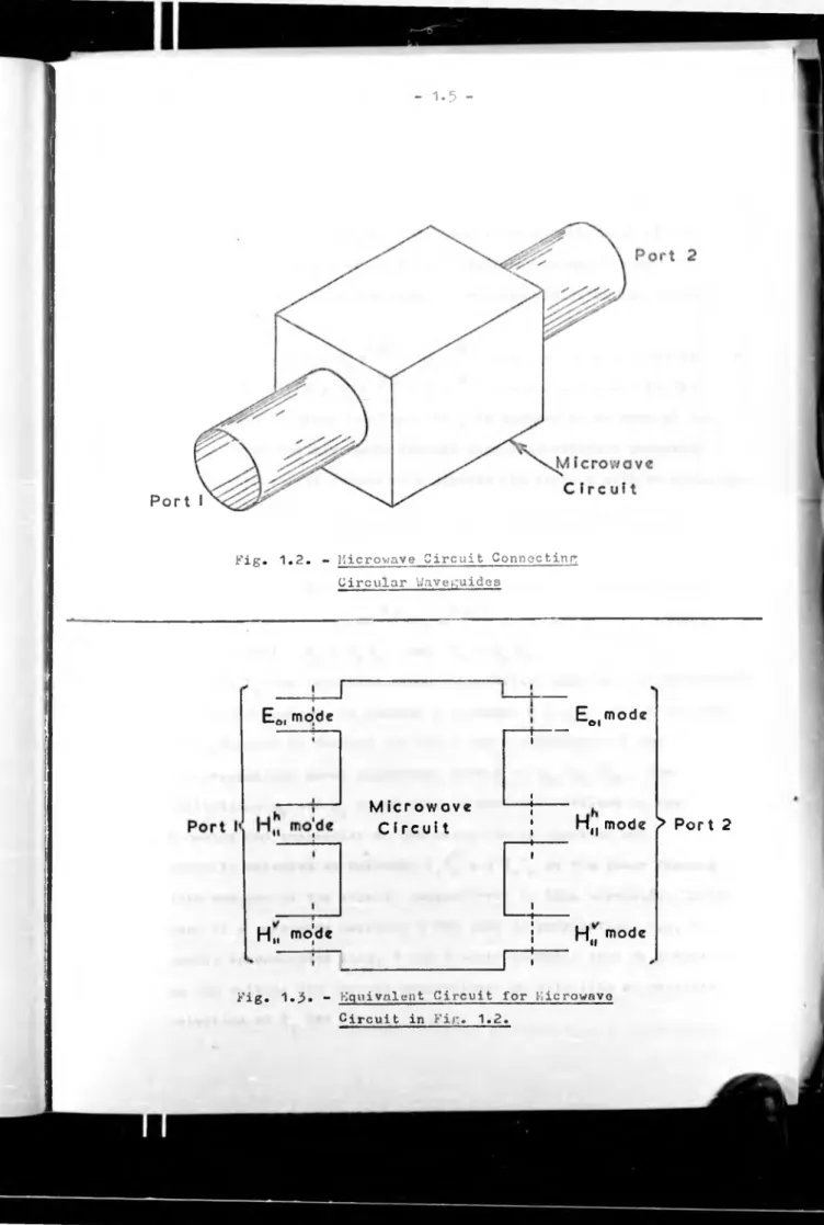
of this is a circular wavep,uide which, in general, may carry, at one frequency, a number of modes at any orientation. This problem may be overcome by considering this type of problem as the
superposition of a number of separate ports on the circuit one port for each mode of propagation in the waveguides connected to the circuit. This is illustrated in Fig. 1.2 where
in the exterior circular waveguides an mode and an mode may be present with the latter mode having a horizontal, H ^ ,
V _
and vertical, component. Thus the 2-port circuit in Fig. 1.2
could be considered as a
6
-port circuit with one port for each mode of propagation in the circular waveguides as shown in Fig. 1.3.1.1.3. Description of Circuit Performance
So far we have arrived at describing a microwave circuit as an n-port network with each port carrying a given mode of propagation in the waveguides connecting it to the exterior. Now it is necessary to define the amplitudes of each mode and to describe the connection between all these modes on all the ports of the microwave circuit.
Initially it is necessary to consider the amplitudes of the electric and magnetic fields of the electromagnetic waves
P o r t
Fig. 1.2. - Microwave Gircuit Connecting Circular Waveguides
E ol mode
J-H „ mo|de
E^.mode
Ol
M i c r o w o v e C i r c u i t
— i— i
i ¡ i i i
i 1 1 1
i_____________________ :
H (| mode ^ P o r t 2
H mode
' 'm
to the direction of propagation aro related by the wave impedance for the waveguide, Z , so that
w
E = Z H for the wave propagating into the circuit + w +
and E = Z H for the wave propagating out of the circuit — w —
with Z^ in general complex to include lossy waveguides or
evanscent modes. Thus the total transverse fields in the waveguide
for this mode is
E = E+ e“^ x + E e Y x --- -- (1.1a) and H = H+ x _ H e V x --- - (1.1b)
for distance x along the line. If x is assumed to be zero at the interface of the microwave circuit with this exterior waveguide then all practical values of x outside the circuit will be negative.
A more convenient way to write equations(1.1) for a
circuit analysis is
V = V e” ^ X + V e y X --- (1.2a)
+ ”
and I a I e ^ X - I e X _ _ _ _ _ _ _ _ _ _ (
1
.2
b) where V = Z I and V = Z I+ o + o
-V, I and Z now represent scalar quantities which may be represented
by complex numbers. In general a voltage, V = g E , and a current, I = g. H,could be defined for the + and - components of the
two propagating waves separately with Zq = ( Ey / g^) . The multipliers gy and g^ would then be constants defined by the
geometry and properties of the waveguide in question and
♦ *
normally selected to maintain V+I+ and V I as the power flowing
into and out of the circuit respectively in this waveguide. In the case of a waveguide carrying a TEM mode of propagation, i.e. a simple transmission line, V and I would normally also be selected as the voltage and current respectively on this line by suitable
selection of g and g..
is to describe the electromagnetic wave or mode amplitudes flowing out of the microwave circuit as a function of the wave or mode amplitudes flowing into the circuit in every waveguide connected
to the circuit. This is termed the scattering parameter description of the circuit and this will be described in detail in section
1
.2
.2
.1.1.4. Practical l-'iircowave Circuits
In this section a number of practical microwave circuits will be described from which a better understanding of the problems involved in the analysis of microwave circuits can be arrived
at.
1.1.4.1. Practical Experience in Circuit Synthesis and Analysis
The first 5 months on the thesis was spent at Microwave Associates Ltd., Luton and during this period experience in the synthesis and analysis of Microwave Integrated Circuits was obtained. The first problem involved the design of an L-band
(1.3)
microwave integrated circuit switch * and this is described
in Appendix A.1. The second problem involved a comparative study of various types of microwave integrated circuit phase shifters^ ^ and this is described in Appendix A.2.
1.1.4.2. Coaxial Plunger
1.8
-/ -/ -/ -/ -/ -/ -/ -/ -/ -/ -/ -/ -/ -/ -/ 777?
7 8 : 9 \
■... - —
'Ss S j/ / S . y s / i
r
± 7
T
7
^ Y /
a
Sf/sW sl
^
2
S m
2
Z ^ P Z z M
2
Z Z Z M Z Z Z Z Z ^ Z Z A
N. B. T h e numbers in c i r c l e s a r e t h e p a r t numbers in the a ss emb l y whilst the o th er s a r e f o r the e q u i v a l e n t c i r c u i t
Fig. 1.4. - Adjustable M icro w ave C oaxial Plunger
Fig. 1.5.- Equivalent C ir c u it for
from an infinite length of coaxial line, for sections
1
to 7t and an inhomogenously filled circular waveguide, for sections8
and9
. Each of these sections can be considered as a simple distributed transmission line within a2
-port network.for a predominately T'»: mode analysis in the coaxial liner,
the connections of the networks in the equivalent circuit can be considered as a direct connection of voltage and current from the port of one network into the next as the wave propagates down the line, e.g. junctions between network
2
and3
»2
and **» ^ and 5 in Fig. 1.5. In the case of the junctions between networks1
and2
and6
,5
and6
and7
the wave propagating down the line has to split between two networks, also at the end of network 7 the line changes from a coaxial line into an inhomogenouslyfilled circular waveguide in which it is assumed that two modes may propagate. Thus the 3-port' network between network 7 and
8
will split the TL3', mode wave into the appropriate amplitudes of these tvjo modes. Similarly the If-port network between networks8
and9
will modify the amplitudes of these two modes as the inhomogenous filling of the waveguide changes. The effects of the discontinuities in the circuit, e.g. change in the field pattern between various radii on the coaxial lines, can usually be taken into account by including a1
-port network, e.g. a shunt susceptance, on the junctions between the networks inquestion.
1.1.^.3» Microwave Integrated Circuit Phase Shifter
F ig .1.6.- M icro w a ve Integrated C ir c u it
P h a s e S h if t e r
rhia equivalent circuit consists of the following
1
) ¡.icrostrip transmission lines for networks2
to1 1
»15
and 15 to 17. N.B. It is often assumed that only a TEt". mode of propagation is present on the microstrip line2
) p.i.n. diodes for networks12
and1
1*.3
) d.c. isolating capacitors for networks 19 and20
.1 . 1 2
I
1
.2
. • ( ... v . oi CHIT :;x.g1.2.1. blips of n-nort networks
In section
1
.1
.h. various types of microwave circuits were presented and broken down for analysis. The complete circuit consisted of a single n-port network which could be broken down into an assembly of n-port networks each one of which was simpler to analyse on its own than the complete circuit. In a number of cases these n-port networks have a simple equivalent or approximateto a simple equivalent circuit, o.g. Tables 1.1 and 1.2. It should be noted that in a number of cases an equivalent circuit may only represent correctly the microwave component over a limited frequency range and often the component values in the
equivalent circuit may vary in a complex manner with frequency.
In the analysis of assemblies of n-port networks, and in the final circuit, we are only interested in the amplitudes of the modes of propagation of the electromagnetic waves on each port of an n-port network. In practice it may be necessary to include
an ideal transformer with unity turns ratio in cascade with each
port on every n-port network to arrive at a more accurate equivalent circuit.
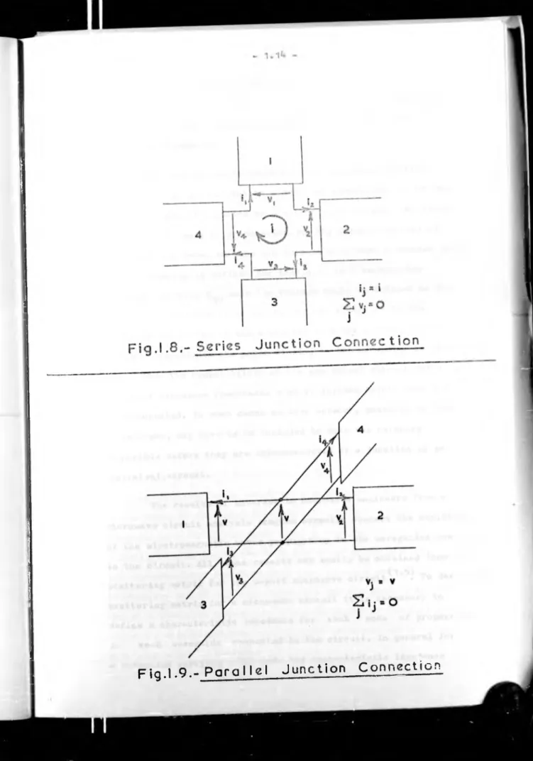
To analyse microwave circuits as an assembly of n-port networks it is necessary to consider how the networks are interconnected at junctions of the networks. There are two basic ways in which networks may be interconnected. These are the series and parallel junction connections as shown in
T ab le . I . I.- Simple I- P o r t Networks
o -r —
1 --- i— 0
i i 11 Z
1 1
!____— °
1
° — t-____ b d
1
— — °
S e r i e s Z
" iH X b d E H I
T ee
S h u n t Z
n V C L
J L _
P h i
Id e a l T ra n s fo r m e r
Table. 1.2.- Simple
T ra n sm is s io n Line
There may be some types of junctions which may be a mixture of
these two types but they can always be broken up into separate series and parallel junctions using
2
-port connecting link networks as necessary.For some microv/ave components an immediate relation
between voltage and current at a junction connection can bo seen either in terms of a series or parallel junction,e.g. for lines carrying a Tiv. mode of propagation. For the interconnection of waveguides the terms voltage and current only have a meaning in so
far as a meaning is defined for them,e.g. in a rectangular waveguide carrying mode the voltage could be defined as the
voltage from the centre of the top of the waveguide to the
centre of the bottom of the waveguide with the current defined so *
that v i represents the power flowing in the waveguide at that point. Thus the compatibility of the equivalent circuits of a number of microwave components must be decided before they are interconnected. In some cases another network, possibly an ideal
transformer, may have to be included to make the networks compatible before they are interconnected at a junction in an equivalent circuit.
The results of interest to microwave engineers from a microv/ave circuit analysis program normally concern the amplitudes of the electromagnetic waves propagating in the waveguides connected to the circuit. All these results can easily be obtained from the scattering matrix for the n-port microwave circuit^”**'^ To derive the scattering matrix for a microv/ave circuit it is necessary to
just defines the ratio of voltage to current between the two conductors of the waveguide, for other nodes in waveguides the definition of tho characteristic impedance is more arbitary but it must be compatible with the voltage and current defined for that mode in the waveguide. In general the characteristic impedance
may be a complex number to allow for lossy propagation in the waveguide or evanscent modes of power transfer.
1.2.2. Wave and P e e r .'.cattering Matrices
For the microwave engineer it is necessary to present
the results of a microwave circuit analysis in the form of a scattering matrix for an n-port network for, in general, a different complex characteristic impedance for each port. The resulting scattering matrix is then in the form :-
b = S a
where b = column vector of reflected wave amplitudes a = column vector of incident wave amplitudes S = n x n scattering matrix
A problem arises in describing the scattering matrix for complex characteristic impedances due to the possibility of two different scattering matrices. One describes the amplitudes
- 1 . 1 8
-From equation (1.8) the power into port i (subscript i) is.-= Re( V. )
■ K l
2
- K l
2
* »If the input ii pedane e of port i is Zq^ then b. = 0 and thus
for any input impedance on port i
Ja.|2 = incident power on port i | • (*■ = reflected power on port i lbil
1.2. ?.. 3- '-'avo/Povn - :cattcrinr Conversion
Equating equations (
1
.5
) and (1
.8
) and rearranging gives1
) Uave to Power Conversion H Z,o o
- 1
j R X
d o o
(1.9)
substituting b and b from equations (l.^b) and (
1
.7
b) givess = ( S R
0
+
i
Xo ) Zo
-1(
1.
10)
2) Power to Wave Conversion
Z
- 1
R o o-j z
" 1
x
L o o
(
1.
1 1)
substituting b and b from equations (1.4b) and (l«
7
b) givesi-s = ( i-s’ Z
0
- J xo )
r
; 1
(
1.
1 2)
It should be noted that if all the terms in Zq are real, i.e. Z = R and X = 0, then both the wave and power scattering
o o o
i • '
parameters are the same, i.e. a = a , b = b and S = S .
1.2.3. Presentation of Results
Scattering Matrix Scattering Matrix Wave Scattering
Parameter, S.^
ij Sij
S
. .
Z. H” 1
for 1/3
iO
03
03
“
(
for i=
3 see|V )
Wave Reflection Coefficient,
TV
s . ,
1 1
( s ’
Z.
- j X. )
R~1
1 1
01
01
01
Voltage Standing Wave Ratio, VSWR.
’
i1 -
\Si ± \1
- | s 41|
1
♦ | s ' |
1
1 1
«1
- \s! |
1
ia* Input Impedance,ZINi
1 + s . .
z
. ---- —
0 1
1 -
s. .
1 1
. . 1* 8“
1 - S liPower Scattering
«
Pararameter
,
S.. Sij ©O OO. .
R.
Z~1
for(
for i=
j seei / i
' i t
Reflection
Coefficient, TV < S i l ao i * J Xo i > K ]
I
s . .
I I
Transducer Gain, PTij
I
R.
Z" 1
S. .I
I
oj oj1 3
IK j l 2
Return Loss, RLi
l( S.
.
R.
+ j X.
) Z- 1
I
| li
01
J
oi03
1
K
1I
2Power Gain, P
Ti.1
K j
' 2PGij
1
-
Rt.
Li 1
- K
jI
2Available Gain,
PTi.i
K , l
2PAij
1
-
rlj 1- K J
2Insertion Gain,
P Iij
|
z .+
z . -21---°A pz < - z \ Ti^
1
01
0
j2
I
Zo i + Zo3
• I
z . - z \
^
•
oi oj•
Insertion Phase, Arg( S. .
) -
Arg(Z)
* -
A
i
* *.j >
for ijij
A r g i s ’^
) +
Are(Z o . + Zo;j)
N.B. The results of gain and return loos are often quoted in dB. To obtain these in dJ3 then use 10 log(power ratio)
their derivation in terna of both the wave and power scattering parameters, "'or the evaluation of t’ ere partii etera -'ill the porti of the microwave circuit are terminated in the characteristic impedance for those ports unless otherwise stated.
Tiie definitioi
5
of the results in Table 1.3 are as follows amplitude of wave reflectedÆ \ . . . , on port i
1) wave scatterin': para, eter, S. . = rr;— -- —--- :-- :--- r~ ° * ’ ij amplitude of wave incident
on port j
amplitude of wave reflected 2) wave reflection coefficient, T\ = --- — ~t--- --- — -- :—
i amplitude of wave incident
3
) voltage standing wave ratio, V3./IÌ. =on port i
maximum electric field alon"; line on port i minimum electric field
k ) input impedance, =
along line on port i
voltage on port i current into port i
amplitude of power wave
. . . reflected on port i
51
power scattering parameter, S. . = --- r-rr— :---x—---y ‘ “ 1 ’ ij amplitude of power wave
incident on port j
6) reflection coeffic
( amplitude of power wave T
"1
... reflected on port i1
amplitude of power wave incident on port ipower out of port i
7) transducer
6
°in « ^ i j ~ power available from port j8
) return loss, R, . =power out of port i Li ~ power available from port i
power out of port i 9) power gain, Pg... = pOWCr into port j'_
maximum power available from port i
„ for anv termination
1 . 2 2
I
1
.
5
. c<>:.1-liT■.: A3 n .;.ii
(.:■
r.ic
..V::
c i x u i t b1.3• 1 - Introduction
If we look at the possible requirements of a prospective
user of computer aided design he would usually like the computer
to design a microwave circuit to fulfil- a set of performance requirements. In fact ideally he would like the computer to
produce a suitable circuit design from a set of performance requirements . This can be done for special cases, e.g. for some filter circuits, where the equations for the synthesis are well
defined for a given type of circuit but for general circuit design this is not possible. In practice the user would have to define or guess an initial circuit topology with the component values in that circuit. Then he could analyse this circuit on the computer to see if it fulfilled his performance requirements. If it did not then the circuit component values could be modified either manually or automatically in an optimisation routine to
try to improve the circuit performance. In very complex circuits the user may prefer to design and analyse each part of the
circuit in turn before analysing the entire circuit.
1.3.2. liicrownve Circuit Description
Ideally one would like to include provision for the entire range of microwave components in a computer program for the
The objective of a circuit analysis procedure would be to provide results describing the circuit performance and, for microwave circuit analysis,it would have to consist of
2
parts as follows:-1) From the data describing each microwave component form its description into an n-port network either in terms of a single matrix describing that n-port network or a simple equivalent circuit within an n<-port network.
2) Use a circuit analysis method to analyse the circuit which now consists of an assembly of n-port networks.
For a circuit analysis on its own it is usually best to supply the user with a table of results of the circuit performance printed out for a set of frequencies defined by the user.
Alternatively if an optimisation procedure is to be used then it is
necessary to analyse the circuit and compare its performance with the desired performance of the circuit from which the optimisation procedure can adjust the circuit component values to try and improve the performance of the circuit.
1.3.,t. Optimisation
In a circuit design it is usually impractical to let the user adjust the circuit component values manually to improve the circuit performance, particularly if a large number of component values may bo adjusted. For this type of work there are a large number of optimisation procedures available which could be used and the main problem into choose the best one(s) to use for the
'\.2‘t
-1.3.5* The Computer Program
The simplest way to use a computer for computer aided design ia on hatch processing using the card or paper tape reader for the input data and the line printer for the results.
Unfortunately the user often meets with problems in using this type of program. He will often make errors in preparing his data and he will normally take a long time to find and correct these errors. Thus often 2 or 3 runs are required on each problem and each run may take several hours, or even days, between the time it is
handed in for a run on the computer and the time it is return with the results of the run. Also all he v.'ill get is the results
in tabular from from v'hich he will often have to plot graphs before he can decide whether the circuit performance is acceptable. Then, if the results of the circuit performance are not satisfactory, he will have to modify the circuit description and rerun the program with the new data.
An improvement to this method is the use of the program interactively on an on-line remote teletype. This has the
advantage that the user can type all his data in directly to the program and have his results printed out directly on the remote teletype. This is extremely slow in terms of real time but if the computer is a multi-access machine then only about
2
to3
times the processor time on batch processing will be used and the user willbe able to see the results immediately after which he can decide
to accept the present design or to try and improve the circuit design.
computer program. In using a remote teletype the user would often make errors in the data and he would like to be able to correct errors without terminating the run. Thus the user would like data checking to be included in the program to enable him to do this. Also he may wish to compose the input data as he types it in. In this case the data would have to be very meaningful to him and ideally he may prefer to use a complete problem orientated
Ijrogramming language for microwave circuit analysis which would bo very easy for him to read and understand the data and would print out the details of any errors in the data for their
immediate correction.
So far the results would still be printed out in a tabular
form . This is not very convenient as it would normally take a long time to decide if the results are acceptable or to decide what to do to improve them by altering the circuit description. This problem could be overcome by the use of a visual display, normally placed next to the remote teletype, on which graphs of the circuit performance could be plotted.
In the programs described in this thesis, particularly
1.26
-1
.
4
. i1!;: : -: ? i ■
. -i
2
:: ?c : r
ic.X'\i
w.:
c ir c u it1.4.1. Introduction
The programs previously written for the analysis of microwave circuits neatly fall into two classes.
The first class consists of the programs written for the analysis of microwave circuits which consist mainly of a cascade
of 2-port networks. A large number of the simpler microwave circuits fall into this class as most microwave circuits involve the propagation of a wave or signal from the input port of the circuit to the output port with the signal being 'processed' by each part of the cascade in turn. It is usually fairly easy to transform this typo of problem into a cascade of
2
-port networks(1.7)
so a chain matrix method of analysis * can be used. In a number of programs using chain matrix analysis the method of analysis has been extended to include branch arms and/or parallel paths of cascades of
2
-port networks on top of the main cascade of2
-port networks in the circuit.The second class consists of programs written entirely for the analysis of lumped element circuits. In this case the circuit consists of a number of branch components connected between nodes in the circuit. Each branch may include a resistor, inductor,
capacitor, independant and dependant voltage and current generators, mutual coupling for inductors etc.. The methods of analysis used
(
*1
8
)are usually a nodal analysis * or, more recently, a mixed mesh (1.9)
generators in the circuit. To maintain continuity some programs ox this type have been extend for use in the microwave region by replacing the microwave components in the circuit by their lumped
element equivalent circuits.
The main points of most of the previous programs for microwave circuit analysis have been outlined here but there is
still a need to consider the ways in which the programs can be used, e.g. data format, results provided, interactive use, etc..
1.^.2. Chain Patrix Analysis Programs M.
6
. !•> tk es i k * m ¿«.vet ».protruiLlll. pr*ytre-ttt .»rJt.
1.^.2.1. m'r.cPH
(
1
.10
)This program was written by ¡’tCl’hun ’ and was designed for the analysis of microwave reflection amplifiers and later
extended for other circuits. It is a low level progx’am written in Algol for an Ixlliott 503 computer. It includes 2-port networks only containing single H, L or C components, stub transmission lines and tunnel diode equivalent circuits. The program will analyse circuits consisting of a cascade of
2
-port networks with branch arms to any level either connected to the main cascade in series or shunc.The order in which the data is read defines the topology of the circuit and this data consists entirely of numbers, except for one title string. Thus the program is difficult to use and very sensitive to data errors. The results are in tabular form giving the frequency response over a frequency range defined by the user with up to
10
possible options included consisting of1 . 2 8
-level program written for a time sharing computer using a remote teletype and the user can interact to a certain extent with the running of the program. The program includes
2
-port networks only containing transmission lines, stub lines and series and shunt i{, L , C combinations of components. The program will handle up to60
networks assembled in a cascade between the input and output ports of the circuit with branch arms, series or shunt connected, and parallel paths, shunt connected only, to a level of3
on the main cascade. The order of the input data defines the topology of the circuit and the input data includes3
letter words to describe the network types and their topology. Command words arc used in the data to control the running of the program and to edit the circuit description. Thus the program is easy to use and not too sensitive to data errors. The output is in tabular form over a frequency range defined by the user with a set number of output options, i.e. VSWH, transmission loss and phase and input resistance andreactance.
medium level program written for a time sharing computer using a remote teletype terminal and the user can interact to a certain extent with the running of the program. The main advantage of this program is the large number of network types in the program including
1.1+.2.3. DI HI ET
This program was written by Parker
(
1.
12)
. It is a low toparallel paths connected either in series or shunt. The order in which the data is read defines the topology of the circuit and the data consists of a title followed by a list of numbers. Thus the data is at a low level with a small amount of data checking in the
program. The results output at each frequency consists of the frequency value followed by up to three selected output options
printed out at selected points in the network.
1.4.3. Electronic Circuit Analysis Programs
1.4.3.1. k c a p
This was possibly the original general purpose electronic (1•13)
circuit analysis program,written by IBM , designed, at least
initially, for batch processing. It is a medium level program and it is complete package including linear, d.c., a.c. and transient analysis for a lumped element circuit and uses a nodal method for the a.c. analysis. The data for the program includes a number of words
and data checking is included. Thus the program is simple to use and the circuit is defined by a number of branches connected between nodes in the circuit with each branch consisting of lumped
components. The results from the program consist of all the
voltages at every node and all the currents in every branch in the circuit. In addition extra facilities are available, e.g. sensitivity
analysis, worst case analysis.
1.4.3*2* h eJAP
31
This program was developed by Redac Software I.td. * for
1.30
-I
developed by Bran.in^ . The circuit to be analysed consists of lumped components t tz . ision lil included as
3
-terminal,2
-port networks described by an admittance or scattering matrix and several electronic components, e.g. transistor equivalent circuits, from a data bank may be include. The input data is at ahigh level including a large number of words with full data checking and the program is thus easy to use. The output is in tabular form over a frequency range defined by the user. Host of the output options included are those of interest to the designer of electronic circuits. Also there are a number of extra facilities included, e.g. sensitivity analysis, worst case analysis, monte carlo analysis and optimisation. A recent addition is that the program can be used on-line interactively on a remote teletype.
1.4.3.3. BELNAP
1.5. COHCLU.S I0H3
Tho objective of this chapter was to outline the way in which the problem of the Computer Aided Design of Microwave
Circuits should be tackled.
Firstly from an investigation into the general form of microwave circuits it was found that the entire microwave circuit could best be described as an n-port network. The results of interest to the microwave engineer in terms of the performance of this circuit is the relationship between the amplitudes of the modes of propagation on the waveguides or transmission lines connected to the ports of the circuit. These amplitudes can be best described in terms of the scattering parameters of the circuit.
The analysis of the circuit itself can be best tackled by breaking the general microwave circuit, as an n-port network, into an assembly of n-port networks. Each of these n-port networks representing a part or component vised in the microwave circuit. Thus it is necessary to analyse an assembly of n-port networks and provide the results in terms of the scattering parameters of the circuit. The methods used so far for the analysis of electronic
circuits including, in some cases, microwave circuits has been the chain matrix method of analysis or the nodal method of analysis. Thus it will be necessary to decide on the beet method of analysis to use for microwave circ iits.
The organisation of a computer program for microwave circuit
- 1 . 3 2
-I
Ref orencos
1.1) C.G. Montgomery, R.H. Dicke, E.M. Purcell, 'Pi’inciples of
Microwave Circuits', Dover, 19&5
1.2) S. Rarno, J.R. Whinnery, T. Van Buzer, 'Fields and Waves in
Communication Electronics', Wiley, 1965, Chapter 4, pp. 228-269
1.3) B.G. Marchent, 'Computer Aided Design of an L-Band M.X.C. Switch', Microwave Associates Ltd., Luton, 1969, Technical Report No. 160, ( see also Appendix A.1 )
1.4) B.G. Marchent, 'A Comparative Study of the Iterative, Hybrid Ring and Switched Line Microwave Phase Shifters', Microwave Associates Ltd., Luton, 1969, private communication,
( see also Appendix A.2 )
1.5) 'S-Parameters - Circuit Analysis and Design', Hewlett Packard,
Application Note No. 95, Sept. 1968
1.6) L. Weinberg, 'Fundamentals of Scattering Matrices', Electro-
Technology (USA), Vol. 80, July 1967, pp« 55-72
1.7) D.A. Calahan, 'Computer Aided Network Design', McGraw-Hill,
1968
, pp. 36-391.8) E. Wolfendale, 'Computer-Aided Design Techniques', Iliffe,
1970, Chapter 2, pp. 15-50
1.9) F.H. Branin, 'Computer Methods of Network Analysis', Chapter 3 in F.F. Kuo, W.G. Magnuson, 'Computer Oriented Circuit Design',
Prentice-Hall, 1969, pp. 71-122
1.10) M.K. McPhun, 'A Computer Program for the Analysis of Branched Distributed and Lumped Circuits', IEE Conference Publication
1.11) P.E. Green, 'General Purpose Programs for the Frequency
Domain Analysis of Microwave Circuits' , IEF.E Trans, on Microwave Theory and Techniques, Voi. MTT-17, No.
8
, August 1969> PP*506-51**-1.12) W.N. Parker, 'DIPNET: A General Distributed Parameter Network Analysis Pi’ogram', IEEE Trans, on Microwave Theory
and Techniques, Voi. MTT-17, No
8
, August 1969, PP **-95-505 1.13) H.M. Valli C.O. Harbourt, 'ECAP: A Matrix-Oriented Approachto Network Analysis', Chapter 1 in G.W. Zobrist, 'Network
Computer Analysis', MacDonald, 1989« PP» 1-77
1.1**-) 'REDAP31: General Circuit Analysis Program (Redacal Version )', Kedacal Manual, Voi. 1, Redac Software Ltd., Tewkesbury
1.15) G.J. Herskowitz, 'Computer-Aided Integrated Circuit Design', McGraw-Hill,
1968
, Chapter1.16) M.A. Murray-Lasso, E.B. Kozemchak, 'Microv;ave Circuit Design by Digital Computer', IEEE trans. Microwave Circuits and Techniques, Voi. MTT-17, Ho.
8
, Aug. 1969*C h o p te r
2
C i r c u i t
A n a ly s is for
2.1. IliTNODPCTION
.in this chapter the method« of circuit anal;, sis which may to used for the small signal linear analysis of microwave circuits in the frequency domain are considered. The objective is to choose the best method of analysis which
:-1) will handle all microwave circuits and components, 2) gives the correct,or at least an accuratesolution
for any meaningful circuit,
3) uses the minimum number of operations and computation time on the computer and
b) is easy to program.
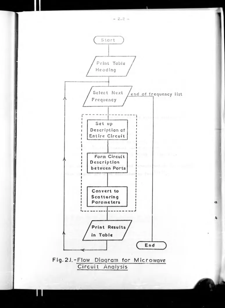
A flow diagram for a microwave circuit analysis program which will produce a table of results of the circuit performance is shown in i’ig. 2.1. The method of analysis is not defined here but the flow diagram is applicable to most methods of analysis. The problems discussed in this chapter are the analysis part of
the flow diagram shown within the dotted lines-in i'ig. 2.1.
The previous programs for the computer aided design of
( S t e r t
)
In thin chapter reference will often be made to the number of operations required in a calculation, lor this an equation lining the term CALC on the left hand side and a list of operatiohs on the right hand side will be given. The CALC equation may also be followed by a TILE equation giving the time for this set of operations in M r . for the Elliott 4130 computer with a 2jUz> store. The meaning of the operations given in the CALC equations and their computation times are given in Appendix A.3. To simplify some of those expressions the times for array access have been ignored.
To compare the performance of the various methods of analysis the computation times have been derived for each method of analysis for two practical examples
:-1) a cascade of n 2-port networks, Fig. 2.4, and 2) a non-contacting coaxial short circuit, Fig. 2.2,
with its equivalent circuit shown in Fig. 2.3.
N.B. Most of the 2-port parameters and transformation for networks