Efficient Hardware Implementation of SHA-3 Candidate
Grøstl using FPGA
Syed Muhammad Adnan
Department of Electrical Engineering,
Pakistan Navy Engineering College, National University of Science and Technology
(NUST), H-12, Islamabad, Pakistan
Arshad Aziz
Department of Electrical Engineering,
Pakistan Navy Engineering College, National University of Science and Technology
(NUST), H-12, Islamabad, Pakistan
ABSTRACT
In 2007 NIST announced a public competition to develop a new cryptographic hash algorithm. This competition was announced due to the fact that in recent years, several successful attacks have been reported against SHA-1, thus raised significant alarming conditions against SHA-2. This new algorithm will replace the SHA-2 and can be used in various security applications in the information infrastructure. This paper focuses on efficient implementation of one of the SHA-3 candidates and round-3 finalist Grøstl on FPGA. The aim of this work is to achieve high throughput to area ratio (TPA) simultaneously by achieving high throughput by considering tradeoff between area and speed. The design is implemented as fully autonomous with both permutations P and Q are executed in parallel, and are equipped with I/O wrapper. The developed hardware has two designs, first with S-box is implemented using Look-Up-Table (LUT) or Distributed Memory and second with S-box implemented as Block RAM (BRAM). The implementation results obtained using virtex-5, when S-box is implemented as LUT has a throughput of 9.360Gbps and occupied 2253 Slices including I/O wrapper, thus achieves TPA of 4.154 and when S-box implemented as BRAM has throughput of 5.565Gbps and occupied 1356 Slices with wrapper, thus achieves 4.104 throughput per unit area (TPA) .
1. INTRODUCTION
A hash function takes data, text or any file and generates compressed hash value of the data, called “digest”. A cryptographic hash algorithm is a hash function that fulfills collision resistance, pre-image and 2nd pre-image resistance properties [1], due to which it is widely used in data security and integrity. NIST organized an open competition similar to AES for SHA-3 [2, 3], to replace SHA-2 for its certain chances to be broken within few years. For this competition NIST received sixty-four entries, but only 51 entries were selected. These selected candidates then on the basis of performance are short listed to 14 and then further shorten to remain only 5. NIST selected these five candidates as SHA-3 finalists which are- Grøstl, BLAKE, JH, Keccak, and Skein. This paper focuses on efficient implementation of Grøstl, SHA-3 finalist, on Virtex 5 FPGA. The design strategy is focused on high throughput to area ratio with tradeoff between area and throughput. Two fully autonomous-parallel designs are implemented, first using only Slices to implement both P and Q permutations with S-Box using look up table (LUT). In second design permutations P and Q are implemented using Slices but S-Box is implemented in BRAM.
This paper is organized as, in section-II, literature review is presented, section-III discuses algorithm specifications, section-IV is about our design approach and methodology, and section-V discusses implemented designs, followed by implementation results in section-VI and in last conclusion and acknowledgement.
2. LITERATURE REVIEW
A lot of research work has been done on hardware implementation of Grøstl-256 [4, 5, 6, 7]. In [8] K. Gaj et.al implemented Grøstl-256 on Virtex-5, in this parallel-fully autonomous architecture with 512 bits data path, they explored three different designs for both high throughput and low area. First design is basic iterative architecture with single stage pipelining, second design used folding and third used unrolling. These implemented designs are totally composed of Slices and no dedicated FPGA resource is used. I/O wrappers are built to implement design. The implementation results are 2906 Slices, 7214Mbps throughput and TPA is 2.48. In [9, 10] E. Homsirikamol et.al, showed their work with the same approach in [8] and uses 1912 Slices to achieve throughput of 6072Mbps and TPA of 3.18. In [11] B. Baldwin et.al, implemented basic iterative architecture on Virtex-5 FPGA, using Combinational Logic only with I/O wrapper for real world interface. Round constants and S-box are implemented using Dedicated ROM and Mix Column is realized using XOR and SHIFT. The results obtained are 2579Slices, 3242Mbps of throughput and TPA of 1.257.
In [12] S. Matsuo et.al used dedicated hardware of FPGA for control and data path. The implementation results have 2616 Slices and throughput of 7885Mbps with TPA of 3.01. In [13] K. Kobayashi et.al, used the same platform and strategy, but results were not too efficient. Slices utilization increases to 4057 and throughput decreases to 5171Mbps and TPA is reduced to 1.27.
In [14] B. Baldwin et.al used strategy of implementation with both Slice LUTs and Dedicated BRAM. The results achieved on Virtex-5 FPGA are 8196 Slices using LUTs only while 4516 Slices using Block RAM (BRAM). By using BRAM not only area is reduced but throughput is also increased and has value of 7310Mbps and for LUTs based approach throughput is 5210Mbps. This reduction in area and increase in throughput of BRAM based design raised its TPA 2.5 times more than LUTs based design.
results of 3183Sluces, 2330Mbps throughput and TPA of the design is 0.73.
This work includes implementation on FPGA only. FPGA based implementations for high TPA can be achieved into ways, first by using throughput optimization and second by using area optimization. This paper targets high TPA with the trade-off between both area and throughput. For throughput optimization parallel architecture using S-box in LUT or Distributed Memory is implemented. For area optimization parallel architecture using S-box in BRAM is implemented.
3. GRØSTL HASH ALGORITHM
Grøstl is submitted to NIST by Gauravaram, it was one of the finalists of SHA-3 competition. It is an iterated hash algorithm, similar to AES. It uses two different permutations, built using large and fixed functions. These permutations are constructed using the wide pipe design strategy, which gives it strong resistance against large classes of cryptanalytic attacks. The wide-pipe construction has the feature that internal state size is significantly larger (twice) than the size of the output [16]. Grøstl has four variants which are referred as Grøstl-n, where n is digest size. Message size is denoted by l, where l can be 512 bits or 1024 bits. For Grøstl-224/256, l is equal to 512 and for Grøstl-384/512, l is equal to 1024. The algorithm consists of compression function and output transformation. Compression function iterates message block m. First message m is padded and split into l bit blocks and is processed sequentially, as given in equation 1.
hi ← f (hi-1, mi) for i=1,….., t (1)
After last message block has been processed the output H (m) of hash function is calculated as given in equation 2,
[image:2.595.359.493.494.684.2]H (m) =Ω (ht) (2) Where Ω is an output transformation function.
Fig 1 shows the Grøstl iterative Merkel Damgård architecture, in which message m is splited into t blocks and then processed iteratively. Output transformation is then applied to this processed message, from which only 256 bits are given out as hash.
3.1 Compression Function
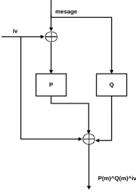
Fig 2 shows the block diagram of Grøstl Compression function f. Functions f has two distinct permutations P and Q; both permutations are applied to the message block. Permutation P is applied after Xoring message block with initial vector IV, while Q permutation is applied only on message block. Grøstl Compression function f is given in equation 3, in which permutated message from P and Q are XORed with initial value h,
f (h, m) = P (h ^ m) ^ Q(m) ^ h (3)
Both permutations are based on Rijndael block cipher, therefore these permutations run for R number of times and consist of four round transformations. These round transformations are Add Round Constant, Sub Bytes, Shift Bytes and Mix Bytes.
Add Constant transformation XORed the round dependent constant with state matrix A, as given in equation 4,
A←A ^ C[i] (4)
Both P and Q permutations have different round dependent constants.
Sub Bytes transformation is same as Rijndael S-box substitution in which each byte of state matrix A is substituted with respective byte from S-box.
Shift Bytes transformation cyclically shifts bytes by specified number of positions to the left within a given row. P and Q have different shifting positions.
Mix Bytes transformation is basically field arithmetic in F256, in which each byte of state matrix A is multiplied by corresponding value of Circulant matrix B in F256 as in equation 5,
A←B×A (5)
Circulant matrix B is =circ (02, 02,03,04,05, 03, 05, 07).
3.2 Output Transformation
Fig 3 shows the block diagram of output transformation “Ω”. It is the final stage of the algorithm, which gives message digest of n-bits. In this stage output from Compression function is further permutated by P block for R number of rounds. Then the permutated value obtained is XORed with the value obtained from Compression function. The last n-bits of this XORed value are selected as digest while the rest of the bits are discarded. For Grøstl-256, n is equal to 256. Output transformation “Ω” function is given in equation 6, where output of P is XORed with the value “x” and then truncated n-bits are selected.
Ω(x) = truncn (P(x) ^ x) (6)
Fig 1: Grøstl Merkel Damgård Construction [16]
P Q
mesage
iv
P(m)^Q(m)^iv
Fig 2: Grøstl Compression Function [16]
4. DESIGN METHODOLOGY
Previously different design methodology were focused on exploring high throughput to area ratio architectures, either by reducing area or by increasing throughput. Three different architectures were discuss in [9], which are parallel processing of P and Q, unrolling of both P and Q and using n-stages pipelining, can be used for high throughput implementation. In unrolling increment in area is too high as compare to throughput, while pipelining can increase latency of the design. For low area interleaved architectures in [13] and folding in [7] can be useful. But for Grøstl, folding does not help significantly and interleaved design approach has higher no of clock cycles and does not meet our requirements for high TPA.
Considering above deduced observations, parallel P and Q processing implementation methodology seems to meet our aim. Parallel design has higher speed and comparable area to interleaved approach. For this approach two different designs are implemented, first based on Slice LUTs and Registers only, second with Slice LUTs and Dedicated BRAM. Fig 4 is the general block diagram of both design approaches. It includes FIFO wrappers, Control unit which is finite state machine (FSM) and Hash unit. Control unit controls FIFO for data input-output and Hash unit for digest computation.
4.1 I/O Wrapper
Data path for Grøstl-256 is 512 bits and no of I/Os in FPGA are limited, thus an I/O wrapper is required. This wrapper serves both as real world interface and data transceiver. For ease the wrapper is implemented using Registers. Due to Slice registers, area of wrapper is also included in the design area, thus its size is carefully chosen. Choosing size of I/O Registers either 64 bits or 128 bits will occupy large no of slices and require less clocks for data buffering. Instead of considering no of clock cycles, the goal is to consider low area for wrapper implementation. For this reason size of I/O Registers are chosen as 32 bits, which reduces area and take only 16 clock cycles to transmit stream of data bits to Hash unit.
4.2 Control Unit
Control unit is designed to control both I/O wrapper and Hash unit, to operate properly. It uses finite state machine (FSM), implemented using Slices. FSM controller Slices are also included in the design area. Finite state machine controls both the counter and combinational control logic. Counter is used to provide round constants for each P and Q permutations. Control logic is used to generate signals to enable input wrapper, to enable both P and Q permutations and to select output of Mux_P and Mux_Q, for data feedback to each permutation in fully autonomous operation. After 10 rounds it resets counter and enables P permutation for output transformation. Then finally it enables output wrapper for hash output.
4.3 Hash Unit
Hash unit is the main unit of Grøstl, consists of Compression function and output transformation. P and Q permutations run in parallel. Sub transformations of Compression function have data path of 512 bits. All sub transformations run in iterative manner, requiring output from previous transformation to generate its output. Mux_P, Mux_Q and Mux_IV are all 512 bits MUXes. Mux_P and Mux_Q are used for output feedback in both P permutation and Q permutation respectively, in fully autonomous design, while Mux_IV is used to select initial vector or previous hash value for XORing with data stream
from input wrapper. Output transformation is done by reusing P permutation only.
5. OUR IMPLEMENTED DESIGNS
Two architectures are implemented using Virtex-5. First architecture is designed by using only Slice LUTs and second architecture using Dedicated BRAM of FPGA. The reason to choose these architectures is to explore a design strategy that is efficient in both throughput and area. The results of the two implementations are compared with respect to throughput and TPA. Slice LUTs based architecture is simple but takes large area due to parallelism. This design has high throughput since it takes one cycle for one complete round. Second design with Dedicated BRAM has low area as compare to first architecture, but itsthroughput decreases by half with respect to first design, as it requires two cycles for one complete round. Both architectures use I/O wrappers for implementation using Software tool Xilinx ISE 13.1. Design codes are written in Verilog HDL. The results are obtained from post, place and route report.
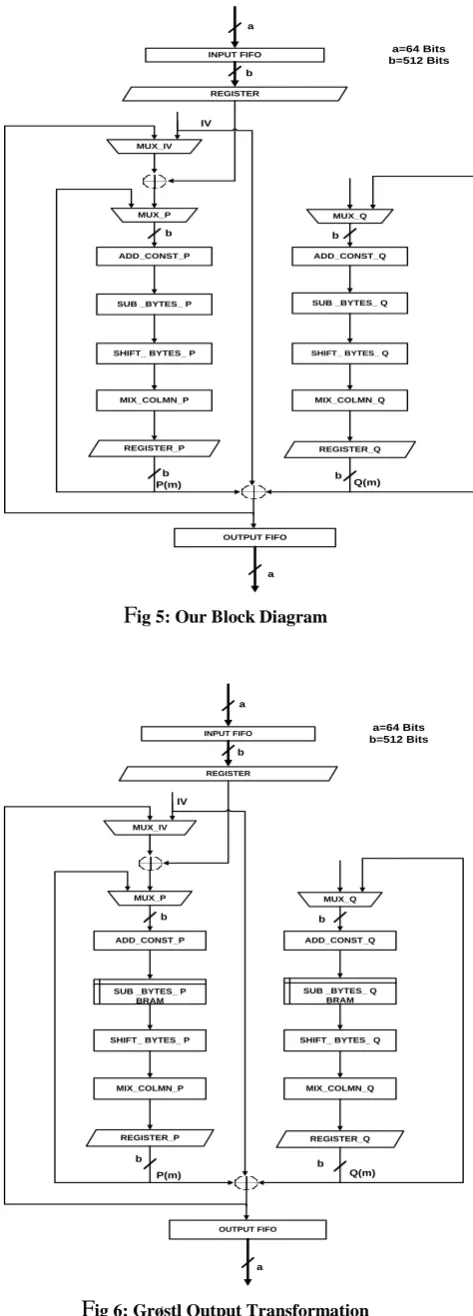
5.1 Slice LUTs Architecture
Fig 5 shows the internal architecture of Slice LUTs design. Slice LUTs based architecture has both P and Q permutations in parallel and fully autonomous. MUX_IV feeds initial or previous hash value to P permutation. MUX_P and MUX_Q feedback data to P and Q permutations respectively in each round. The sub transformations of each permutation are almost similar, except Add Constant and Shift Bytes. The data path between all sub transformations is 512 bits.
P MUX_O
n-BITS x
P(x)^x
[image:3.595.330.523.419.714.2]Fig 3: Grøstl Output Transformation [16]
CONTROL UNIT
(FSM) HASH UNIT
INPUT FIFO
OUTPUT FIFO HASH DATA
HASH CONTROL CLOCK
CLOCK
C
L
O
C
K
F
ig 4: Our Block Diagramdata bytes are transformed by Sub Bytes in one clock due to parallel 64 sub-modules. Shift Bytes is the only round transformation that takes no Slices, since it is just rewiring of data bytes from Sub Bytes. The Mix Column is combinational logic based matrix multiplication and addition in finite field of F256. The finite filed polynomial used is 0x11B. 64 bits of data
are input to the each Mix Column module for multiply and additions with Circulant matrix B. Thus total 64 modules are implemented in parallel to transform the complete message in a single clock.
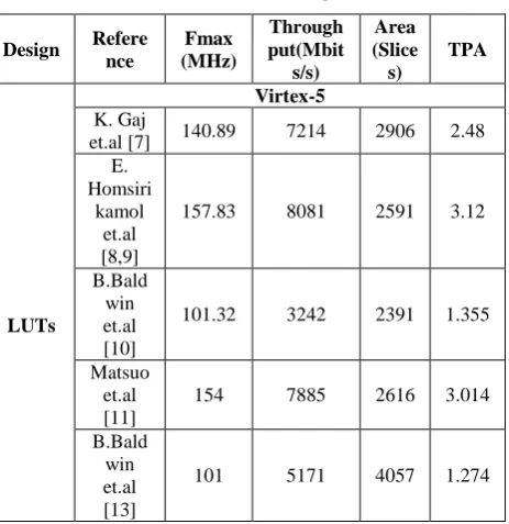
[image:4.595.317.554.73.732.2]5.2 BRAM Based Architecture
Fig 6 shows the internal architecture of BRAM based design.
BRAM based design architecture has both P and Q permutations in parallel. MUX_IV feeds initial or previous hash value to P. MUX_P and MUX_Q feedback data for P and Q permutations respectively. These MUXes serve to feedback the results of previous round to the next round, in fully autonomous design. The sub transformations of each permutation are almost similar, except Add Constant and Shift Bytes. The data path between all sub transformations is 512 bits. In Add Constant the round constants are XORed with data bytes and results are stored in Registers. The Sub Bytes are implemented using BRAM; this method is chosen to decrease the Slice LUTs require to implement 64 S-boxes. There are 64 BRAM modules for S-box is instantiated for 64 bytes of data. This change considerably reduces the no of Slices by almost near to half the value of LUT based implementation. But the clock cycle requirement is increased by twice, since BRAM requires two clocks for data output. One clock delayed data is then SHIFTed by Shift Bytes, which takes no Slice. The Mix Column is combinational logic based matrix multiplication in finite field of F256. The finite filed polynomial used is 0x11B. The data bytes in the group of eight bytes are multiplied by Circulant matrix B. Each byte in the group is multiplied with its corresponding value in the Circulant matrix B. These multiplications are done using SHIFT and XOR. All the data bytes are transformed in one cycle, due to 64 Mix Column sub-modules.
6 IMPLEMENTATION RESULTS
Implementation results of both designs are based on Grøstl-256. Target device of implementation is Xc5vlx155t-3ff1136 of Virtex-5 FPGA. This device is chosen for its suitability in both fair comparison with previous results and also for post, place and route implementation of both designs. Both design results include 32 bits shift register I/O wrapper. The no of clock cycles for throughput is exclusive of no of clock cycles of wrapper function but the area of wrapper is included in area design, since it uses Slices. The maximum clock frequency Fmax obtained from post, place and route static timing report and verified by post, place and route simulation. Table.1. gives overview of percentage of area (Slices) of each individual sub transformation in both permutations after synthesis, for Xc5vlx155t-3ff1136 device.
Table 1. Percentage of usage of Sub-Transformations
INPUT FIFO
MUX_IV
MUX_Q
ADD_CONST_P
MIX_COLMN_P SHIFT_ BYTES_ P
SUB _BYTES_ P
REGISTER
REGISTER_P
OUTPUT FIFO MUX_P
ADD_CONST_Q
MIX_COLMN_Q SHIFT_ BYTES_ Q SUB _BYTES_ Q
REGISTER_Q
IV
Q(m) P(m)
b
a a
b
b b
b
a=64 Bits b=512 Bits
F
ig 5: Our Block DiagramINPUT FIFO
MUX_IV
MUX_Q
ADD_CONST_P
MIX_COLMN_P SHIFT_ BYTES_ P
REGISTER
REGISTER_P
OUTPUT FIFO MUX_P
ADD_CONST_Q
MIX_COLMN_Q SHIFT_ BYTES_ Q
REGISTER_Q
IV
Q(m) P(m)
b
a a
b
b b
b
a=64 Bits b=512 Bits
SUB _BYTES_ P BRAM
SUB _BYTES_ Q BRAM
F
ig 6: Grøstl Output TransformationPercentage of Usage Design Total(Slices) Percentage of
Usage
Add Constant 44 0.04%
Sub bytes 2048 2.14%
6.1 Results of Slice LUTs
Slice LUTs implementation has highest throughput, i.e. 9.36 Gbps. The maximum clock frequency achieved is 182.8MHz. The occupied area is 2253 Slices including wrapper. The high throughput achieved because the latency is low in design. The TPA achieved is 4.15. Which is highest reported TPA, to the best of our knowledge, in all round 3 implementations published in SHA-3 Candidate Conference in March 2012.
6.2 Results of BRAM
[image:5.595.312.550.81.258.2]BRAM design implementation is carried out on round 3 specifications. In this design area is significantly reduced due to S-box implementation in BRAM. The area obtained with I/O wrapper is 1356 Slices. The maximum frequency achieved is 217.4 MHz, which is more than slice LUTs design. But the throughput is moderate due to one clock cycle latency in the design and the value achieved is 5.565Gbps. The TPA achieved is almost equal to the TPA of slice LUTs design i.e. 4.104. The TPA obtained is also highest reported using BRAM based S-box design in round-3, according to our best knowledge.
[image:5.595.58.287.318.396.2]Table 2 Our Implementation Results of Grøstl-256
Table.2 compare our results to that are obtained using Virtex-5 and is much better than other results that are summarized in Table 3 and Table 4. Table 3 show previous results of Slice LUTs implementation using Virtex-5. Table 4 summarizes BRAM based results using both Spartan-3 and Virtex-5.
Table 3 Previous LUTs Design Results
Design Refere nce
Fmax (MHz)
Through put(Mbit
s/s)
Area (Slice s)
TPA
LUTs
Virtex-5
K. Gaj
et.al [7] 140.89 7214 2906 2.48 E.
Homsiri kamol et.al [8,9]
157.83 8081 2591 3.12
B.Bald win et.al [10]
101.32 3242 2391 1.355
Matsuo et.al [11]
154 7885 2616 3.014
B.Bald win et.al [13]
101 5171 4057 1.274
Design Fmax
(MHz)
Throughput (Mbits/s)
Area
(Slices) TPA
LUTs 182.8 9360 2253 4.154
Block
RAM 217.4 5565.4 1356 4.104
[image:5.595.56.288.473.712.2]0.04
Table 4. Previous Block RAM Results
Design Referen ce
Fmax( MHz)
Throughpu t (Mbits/s)
Area (Slic es)
TPA
Block RAM
Virtex-5
B.Baldw in et.al [13]
142.87 7310 4516 1.61 8
Spartan-3
B.Baldw in et.al [13]
71.53 3660 4827 0.75
Junk B. Reith
[15]
54 2764 5693 0.48
5
7. CONCLUSION
Comparison of this work with previous results in table 3 and 4 shows that the implemented designs have the highest reported throughput per unit area TPA in round-3 implementation, to the best of our knowledge. Secondly Table2 Shows highest reported throughput Tp with respect to all other results in Table 3.
8. REFERENCES
[1] “Cryptographic Hash-Function Basics: Definitions, Implications, and Separations for Preimage Resistance, Second-Preimage Resistance, and Collision Resistance”, Department. Of Computer Science, University of California, Davis, California, 95616, USA, Appears in 11th International Workshop, Fast Software Encryption (FSE 2004), Delhi, India, February 5-7, 2004, LNCS
3017, pp. 371-388, 2004.
www.cs.ucdavis.edu/~rogaway/papers/relates.pdf
[2] National Institute of Standards and Technology (NIST), “Cryptographic Hash Algorithm Competition, Federal Register, Vol. 72, No. 212, Friday, November 2, 2007, Notices http://csrc.nist.gov/groups/ST/hash/sha-3/index.html
[3] National Institute of Standards and Technology. Cryptographic Hash Project, 2007. Federal Register, Vol. 72, No. 212, Friday, November 2, 2007, Notices. Available online at http://www.nist.gov/hash-competition. [4] SHA-3 Hardware Implementations:
http://ehash.iaik.tugraz.at/wiki/SHA-3_Hardware-Implementations
[5] SHA-3 Hardware Implementation, Cryptographic Engineering Research Group, George Mason University, Washington,
http://cryptography.gmu.edu/research/index.php
[6] SHA-3 HARDWARE IMPLEMENTATION, Research Center for Information Security http://www.rcis.aist.go.jp/project/index-en.html
[7] Performance Evaluation of SHA-3 Candidates in ASIC and FPGA, Center for Embedded Systems for Critical Applications (CESCA), ECE, Virginia Tech, available at http://rijndael.ece.vt.edu/sha3/relatedwork.html
[image:5.595.50.289.473.714.2]Vol. 2012 (2012), p. 368. The third SHA-3 candidate conference, Washington, DC, 22-23 March 2012, pp. 57-75.
[9] E. Homsirikamol, M. Rogawski, and K. Gaj, "Throughput vs. Area Trade-offs in High-Speed Architectures of Five Round 3 SHA-3 Candidates Implemented Using Xilinx and Altera FPGAs," LNCS 6917, Cryptographic Hardware and Embedded Systems workshop, CHES 2011, Nara, Japan, Sep. 28-Oct. 1, Lecture Notes in Computer Science, Volume 6917, pp. 491-506 ,2011. [10] E. Homsirikamol, M. Rogawski, and K. Gaj, “Comparing
Hardware Performance of Round 3 SHA-3 Candidates using Multiple Hardware Architectures in Xilinx and Altera FPGAs”, ECRYPT II hash workshop 2011,Tallinn, Estonia, May 19-20, 2011, pp. 1-15.
[11] B. Baldwin, N. Hanley, M. Hamilton, L. Lu, A. Byrne, M. O’Neill and W.P. Marnane, “FPGA Implementations of the Round Two SHA-3 Candidates,” The Second SHA-3 Candidate Conference, Santa Barbara, pp. 1-18(2010), Aug. 23-24, 2010.
[12] S. Matsuo, M. Knezevic, P. Schaumont, I. Verbauwhede, A. Satoh, K. Sakiyama, and K. Ota, “How Can We Conduct Fair and Consistent Hardware Evaluation for SHA-3 Candidate?” The Second SHA-3 Candidate Conference, 2010, Santa Barbara, pp. 1-15(2010), Aug. 23-24, 2010.
[13] Kazuyuki Kobayashi, Jun IkegamiS. Matsuo, K. Sakiyama, and K. Ohta, “Evaluation of Hardware Performance for the SHA-3 Candidates Using SASEBO-GII,” The Second SHA-3 Candidate Conference, 2010, Aug. 23-24, 2010, pp. 18-25.
[14] Brian Baldwin, Andrew Byrne, Mark Hamilton, Neil Hanley, Robert P. McEvoy, Weibo Pan and William P. Marnane “FPGA Implementations of SHA-3 Candidates: CubeHash, Grøstl, LANE, Shabal and Spectral Hash”, Department of Electrical & Electronic Engineering, Claude Shannon Institute for Discrete Mathematics, Coding and Cryptography, University College Cork, Cork, IRELAND, 12th Euro micro Conference on Digital System Design, Architectures, Methods and Tools, 2009, 27-29 Aug. 2009 , pp. 783 – 790,
[15] Jungk, B., Reith, “On FPGA-based implementations of Grøstl”. International Conference on Reconfigureurable Computing and FPGAs, 2010, pp.316-321.
[16] P. Gauravaram, L. R. Knudsen, K. Matusiewicz, F. Mendel, C. Rechberger, M. Schl¨affer, and S. S. Thomsen. Grøstl- a SHA-3 candidate Submission to NIST (Round 3), University of California Santa Barbara, Santa Barbara, 2011. Available: http: http //www.groestl.info (2011/11/25).
[17] D. Canright. A Very Compact S-Box for AES. In J. R. Rao and B. Sunar, editors, CHES, volume 3659 of LNCS, pages 441-455, Springer, 2005
[18] Edwin NC Mui. Practical Implementation of Rijndael S-Box Using Combinational Logic. Available at http://www.xess.com/projects/Rijndael_SBox.pdf [19] Vincent Rijmen, “Efficient implementation of the
Rijndael S-box”, Katholieke University Leuven, Dept. ESAT. Belgium.
![Fig 3: Grøstl Output Transformation [16]](https://thumb-us.123doks.com/thumbv2/123dok_us/8101371.787984/3.595.330.523.419.714/fig-grostl-output-transformation.webp)