A Compact Microstrip Crossover Based on Capacitively-Loaded
Artificial Transmission Lines Branch-Line Sections
Jordi Verdu*, Endika Bernaola, and Pedro de Paco
Abstract—This paper presents a compact size crossover device based on the cascade of branch-line sections. With the aim of reducing its size, some of the transmission lines of the structure have been replaced by its equivalent artificial transmission line (ATL). The obtained size reduction is above 30%, and the electrical performance of the proposed structure presents an isolation better than 20 dB in a F BW = 34.5% and a crossover bandwidth better than 2 dB of F BW = 51.5%. Also the good magnitude and phase balance performance must be highlighted.
1. INTRODUCTION
The design of microstrip circuits in the range of microwave frequencies normally requires the cross between two lines with high isolation between them, which is commonly known as crossover [1]. Traditionally, the crossover of signals was achieved by means of air bridges or multilayer substrates [1, 2]. However, the fabrication processes for those non-planar structures present a big complexity and also increase the cost. On the other hand, the use of a branch-line coupler has also been proposed in a crossover design, as it is the case of the work in [3], where a dual-band planar crossover is achieved using a two-section branch-line structure. The cascade of branch-line sections also allows the achievement of a better operation bandwidth as discussed in [4], where structures with several sections are presented to demonstrate the concept; however, the impedance of the RF ports is different from the 50 Ohm reference impedance. This situation requires phase control on the reflection coefficient, and it may cause matching problems when it must be connected to other systems. In this work, a compact crossover based on the cascade of branch-line couplers is proposed. Here, the access RF ports are matched to the reference impedance. In order to obtain a compact structure, the transmission lines of the structureare replaced by capacitively-loaded artificial transmission lines (ATL) [5] resulting in a significant size reduction. This area minimization allows the inclusion of an extra section in order to improve the bandwidth performance substantially.
2. THEORETICAL ANALYSIS
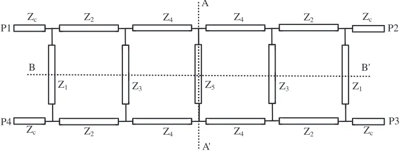
The proposed basic structure for the crossover is shown in Fig. 1. The structure consists of the cascade of a 4-section branch-line coupler which is a good tradeoff between occupied size and achievable transmission bandwidth. Taking into account the symmetry plane given by A-A’ and B-B’, the odd-even mode analysis can be carried out, where the scattering parameters of the structure can be expressed as a function of the even and odd components [6],
s11=
Γee+ Γeo+ Γoe+ Γoo
4 s21=
Γee−Γeo+ Γoe−Γoo
4
s31=
Γee−Γeo−Γoe+ Γoo
4 s41=
Γee+ Γeo−Γoe−Γoo 4
(1)
Received 14 April 2017, Accepted 20 May 2017, Scheduled 19 June 2017 * Corresponding author: Jordi Verdu Tirado ([email protected]).
Zc Z2 Z4 Z4 Z2 Zc
Zc Z2 Z4 Z4 Z2 Zc
Z1 Z3 Z5 Z3 Z1
A A' B B' P1 P2 P3 P4
Figure 1. Crossover basic topology based on the cascade of 4-section branch line couplers.
where
Γee,eo,oe,oo= Y0−Yee,eo,oe,oo
Y0+Yee,eo,oe,oo
(2)
Y0 is the reference admittance, and Yee, Yeo, Yoe, and Yoo are the input admittances of each reduced
network. The analysis of the different four subnetworks given by the symmetry of the structure results in the next even and odd admittances,
Yee= j
Z42
Z1Z3−Z22
+ 2Z5Z22Z3
Z1Z22
2Z5Z3−Z42
; Yeo=−j
Z1Z3−Z22
Z1Z22
Yoe=−
jZ2 4
Z1Z3−Z22
+ 2Z5Z22Z3
Z1Z22
2Z5Z3−Z42
; Yoo =
jZ1Z3−Z22
Z1Z22
(3)
In order to obtain the design equations, perfect matching and isolation are required, so S11 = S12 = S14= 0. The passive and lossless characteristics of the structure entail the crossover state, i.e.,S13= 1.
By a proper combination of equations in Eq. (4) to accomplish the matching and isolation conditions, we can obtain the next relations,
Γee+ Γoe= 0; Γee+ Γeo= 0; Γee−Γoo = 0; (4) However, from the analysis of the structure Γeo =−Γoo, the set of conditions in Eq. (4) is reduced to
two equations. Using Eqs. (3) and (4), we can fix the values of impedances Z1 and Z3. On the other
hand, assuming the symmetry of the structure, we can force the condition Z1 = Z5. Therefore, the
values of the impedances can be calculated as,
Z1 =Z5 = Z0Z 2 2 Z3+Z22
Z3 =Z0
⎛ ⎝Z42
2 −Z
2 2 −
Z4 4 + 4Z24
2
⎞ ⎠
(5)
At this point, we have defined three out of the five required impedances. In order to obtain the values of Z2 and Z4, an algorithm is developed, which calculates the impedance set for the maximum
achievable isolation bandwidth, for a level below 20 dB, as a function of frequency. The obtained maximum bandwidth is found to be around 35%, in agreement with the results in [4], although in this work, port access lines with reference impedance Z0 = 50 Ω are used. The design center frequency is f0 = 2.5 GHz. A fine tunning in the impedance values is carried out to have a better balance in the
Table 1. Impedance values for the basic structure.
Zc Z1 Z2 Z3 Z4 Z5
50 Ω 93.2 Ω 40.3 Ω 54.1 Ω 46.7 Ω 84.2 Ω
2.1. Compact Structure Based on ATL Lines
With the aim of reducing the size of the circuit, artificial transmission lines (ATL) are used [5]. Fig. 2 shows the scheme of the proposal, where a transmission line is divided in cells (dashed square), loading each with a capacitanceCpor its equivalent using open-circuit stubs. By doing this, the effective length
of the transmission line can be significantly reduced. This technique is valid when the dimension of the cell (dAT L and lStub) are much smaller than the wavelength, which is approximately less thanλ/10.
Cp
dATL
lStub
Figure 2. Stub-loaded Artificial Transmission Line (ATL).
The basic cell of a transmission line given byR,L andC is first considered, where capacitance Cp
is in shunt withC at each cell. Therefore, the characteristic impedance and phase velocity of the ATL cell can be calculated as,
Z0AT L = L
C+dCp AT L
; vpAT L=
1
L
C+dCp AT L
(6)
dAT L being the length of the cell which determines the periodicity of the structure. Therefore, the
value of dAT L can be calculated for a given number of sections N, and the electrical length of the
transmission line must be equal to the electrical length of the ATL lineφAT L. Thus, the size of the cell
can be determined as,
dAT L= Z0AT LφAT LvpAT L
Z0N ω0
(7)
whereZ0 corresponds to the characteristic impedance of the transmission line.
The value of capacitance Cp can be obtained by the combination of Equations (6) and (7). The
equivalence between a shunt capacitor and shunt open-circuit stub is very well known. Therefore, the length of the stublStub can be obtained from the Cp value since,
ω0Cp =
1
Z0Stub
tan
ω0 vpStublStub
where Z0Stub and vpStub are the characteristic impedance and phase velocity of the stub transmission
lines. The width of the stub line is related with the width of the main ATL transmission line, which at the same time is related to the number of sections N. As a design rule, it is desirable that the space between stub lines is less than 3h,h being the substrate thickness, in order to avoid undesirable couplings. With this consideration, the rest of the parameters may be chosen depending on the design and technological limitations. For example, the use of a lower impedance of the main ATL line leads to a lower value oflStub for the stub but a higher value ofdAT L, which is not desired for the size reduction.
In case that the obtained value of lStubis too high, one solution consists in including open-circuit stubs
on both sides of the transmission line. By doing this, the total capacitance per cell is reduced to half, leading to an extra length reduction.
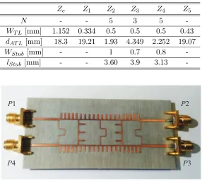
3. FABRICATION AND MEASUREMENT
The proposed device, shown in Fig. 3, is fabricated on a Rogers4003 substrate, with relative permittivity
r= 3.38, thickness h= 508µm and loss tangent δ = 0.0027. The dimensions of the device, as well as
the used sections, are shown in Table 2. As can be seen, neitherZ1 norZ5 is replaced by its equivalent
ATL line since the resulting width leads to a technological constraint. The solution is to use a simple meander taking advantage of the available space. The lines withZ2 andZ4 are substituted by an ATL
line with N=5 sections, while N = 3 sections are used for the equivalence of the line with Z3. The
resulting size of the proposed device presents a size reduction of 30.5% in terms ofλcompared with the 4-sections device in [4].
Table 2. Proposed device dimensions.
Zc Z1 Z2 Z3 Z4 Z5
N - - 5 3 5
-WT L [mm] 1.152 0.334 0.5 0.5 0.5 0.43
dAT L [mm] 18.3 19.21 1.93 4.349 2.252 19.07
WStub[mm] - - 1 0.7 0.8
-lStub [mm] - - 3.60 3.9 3.13
-P1 P2
P3 P4
Figure 3. Resulting fabricated device.
The measured S-parameters are shown in Fig. 4. From the point of view of matching and isolation, the fabricated device presents a rational bandwidth F BW = 46.5% for the matching, and
F BW = 34.5% for the isolation between ports 1 and 2, for 20 dB specifications. If the obtained performance is compared with N = 2 sections, which occupies an equivalent area, the achievable bandwidth increases from 9% to 34.5%. For the crossover, the obtained rational bandwidth is
Figure 4. MeasuredS-parameters of the proposed device.
(a) (b)
Figure 5. (a) Measured magnitude balance and (b) phase balance between RF ports 1-3 and 2-4.
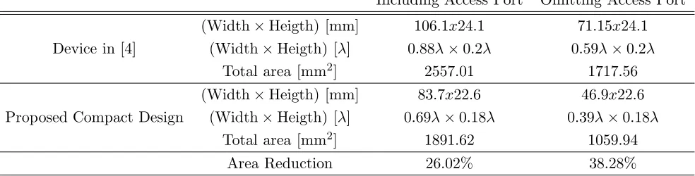
Table 3. Size reduction comparison with the 4-sections device in [4].
Including Access Port Omitting Access Port
(Width×Heigth) [mm] 106.1x24.1 71.15x24.1 Device in [4] (Width×Heigth) [λ] 0.88λ×0.2λ 0.59λ×0.2λ
Total area [mm2] 2557.01 1717.56 (Width×Heigth) [mm] 83.7x22.6 46.9x22.6 Proposed Compact Design (Width×Heigth) [λ] 0.69λ×0.18λ 0.39λ×0.18λ
Total area [mm2] 1891.62 1059.94
presents a wide-band performance in terms of magnitude and phase balance in the crossover state. In this case, as shown in Fig. 5, the obtained relative bandwidth for a difference below ±0.05 dB is
F BW = 63.5% (Top), while for a phase balance below 2◦ it isF BW = 55.1% (Bottom). Table 3 shows the comparison, from the size point of view, between the 4-section branch-line design developed in [4] and the compact structure developed in this work. It must be highlighted that the access lines in [4] are not designed at Zc = 50 Ω; therefore, the direct comparison is not appropriate. However, with the
aim of having a clearer idea, the comparison is shown if these access lines are considered, or if they are omitted. The obtained size reduction is 26.02% in the case of considering such lines, or 38.28% if they are omitted.
4. CONCLUSIONS
A compact microstrip crossover based on the cascade of N branch-line sections is proposed. In order to get a size reduction, the transmission lines of the structure are replaced by their equivalent Artificial Transmission Line (ATL), achieving a size reduction of 30% with respect the conventional structure. To do this, the theoretical development is shown, as well as the required design equations. The electrical performance of the proposed device presents a F BW = 34.5% in terms of isolation and 51.5% in the crossover state. The observed performance in terms of magnitude and phase balance must also be highlighted. In the first case, F W B = 58% for the magnitude balance, and F BW = 31.2% for the phase balance.
ACKNOWLEDGMENT
This work was supported in part by the Spanish Ministerio de Econom´ıa y Competitividad under grant TEC2015-69229-R.
REFERENCES
1. Horng, T. S., “A rigorous study of microstrip crossovers and their possible improvements,” IEEE Transactions on Microwave Theory and Techniques, Vol. 42, 1802–1806, 1994.
2. Liu, W., Z. Zhang, Z. Feng, and M. F. Iskander, “A compact wideband microstrip crossover,”IEEE Microwave and Wireless Components Letters, Vol. 22, 254–256, 2012.
3. Lin, F., Q. X. Chu, and W. Wong, “Dual-band planar crossover with two section branch-line structure,” IEEE Transactions on Microwave Theory and Techniques, Vol. 42, 2309–2316, 2013. 4. Yao, J., C. Lee, and S. P. Yeo, “Microstrip branch-line couplers for crossover application,” IEEE
Transactions on Microwave Theory and Techniques, Vol. 59, 87–92, 2011.