ABSTRACT
HANGEKAR, ROHAN CHANDRAMOHAN. A Multi-Channel Power Controller for Actuation and Control of Shape Memory Alloy Actuators. (Under the direction of Dr. Stefan Seelecke).
The use of „multifunctional‟ Shape Memory Alloy wires as embedded actuators and sensors has been proposed for numerous novel applications. The SMA wires are actuated as a result of the Joule heating induced by passing electric current through it. The resistance of the SMA wire can simultaneously be measured during its actuation enabling it to be used as sensor that relates to the strain and temperature of the wire. In order to control actuation stroke from the SMA wire, the Joule heating (electric power supplied to the SMA wire) of the wire needs to be controlled. Therefore, a multi-channel power controller system has been developed that simultaneously controls the power supplied to six different SMA wires and measures the resistance of these wires during excitation.
The multi channel power controller system comprises of a host computer with LabVIEW software, a National Instruments Field Programmable Gate Array (FPGA) card, a custom built electronic device and a DC power source. The control algorithm adapts to the non linear and hysteretic behavior of the SMA actuator and adjusts the pulse width modulated voltage across it to maintain the desired value of power in the actuator. The controller also gives the resistance of SMA actuator as a feedback. It is therefore envisioned that feedback position control of these actuators can be implemented without the necessity of additional sensor. The system has a software interface in LabVIEW which enables a user to control various parameters in the functioning of this system and to monitor the results.
A Multi-Channel Power Controller for Actuation and Control of Shape Memory Alloy Actuators
by
Rohan Chandramohan Hangekar
A thesis submitted to the Graduate Faculty of North Carolina State University
in partial fulfillment of the requirements for the degree of
Master of Science
Mechanical Engineering
Raleigh, North Carolina 2010
APPROVED BY:
_______________________________ ______________________________
Dr. Paul Ro Dr. Gregory Buckner
________________________________ Dr. Stefan Seelecke
ii
DEDICATION
iii
BIOGRAPHY
iv
ACKNOWLEDGEMENTS
First and the foremost, I would like to express my gratitude to my advisor, Dr. Stefan Seelecke for his motivation, guidance, patience and support through the thick and the thin. It has been an excellent learning experience while working with him.
I would also like to thank Dr. Paul Ro and Dr. Gregory Buckner for the great courses they taught me during my graduate study and for being on my committee.
Special thanks to Dr. Alexander York for teaching me several things during the last year and half, for making my life easier while working in LabVIEW and for correcting my papers and poster. I would also like to thank Stephen Furst for his regular help and for motivating me to work efficiently. I am also thankful to all the other members of Adaptive Structures Lab - Gheorghe Bunget, Micah Hodgins, Nicole Lewis, Aseem Deodhar and Matthew Pausley, for making our lab the best place to study and work!
My special thanks to all my friends here in Raleigh for making my stay at NC State enjoyable and memorable.
v
TABLE OF CONTENTS
LIST OF TABLES ... viii
LIST OF FIGURES ... ix
Chapter 1 Introduction ... 1
1.1. Motivation and Background ... 1
1.2. Review of Control Strategies used for Shape Memory Alloy Actuators ... 3
1.3. Scope of Research ... 4
1.4. Thesis Outline ... 5
Chapter 2 Shape Memory Alloys ... 6
2.1. Background ... 6
2.2. Phase Transformations in the SMA Material ... 6
2.2.1. Shape Memory Effect ... 9
2.2.2. Superelasticity ... 10
2.3. Actuation using SMA ... 11
2.4. Advantages and Limitations of SMA ... 11
2.5. Voltage Control, Current Control and Power Control ... 12
2.5.1. Voltage Control ... 12
2.5.2. Current Control ... 13
2.5.3. Power Control ... 15
2.5.4. Power Control using a Voltage Source ... 16
2.5.5. Power Control using a Current Source ... 18
2.5.6. Selection of Power Control Scheme ... 19
Chapter 3 Basic Concept of Power Controller ... 20
3.1. Functional Requirements of the System ... 20
3.2. Modular Decomposition ... 21
3.3. Selection of the Modular Components ... 22
3.3.1. Control and Data Acquisition Module ... 22
vi
3.3.3. Software ... 24
3.4. Concepts behind controlling power ... 26
3.5. Algorithm of power control ... 27
3.6. Complete Overview of the System ... 28
Chapter 4 Implementation ... 31
4.1. Controller Module Implementation ... 31
4.1.1. Hardware ... 31
4.1.2. I/O Resource Allocation ... 32
4.1.3. FPGA Programming ... 33
4.1.4. Current Calibration Program on FPGA ... 34
4.1.5. Power Control Program on FPGA ... 35
4.1.6. Calculated Examples ... 41
4.1.7. Limiting Values of Active Number of Points ... 42
4.2. Hardware Module Implementation ... 43
4.2.1. Operational Amplifier ... 47
4.2.2. MOSFET as a Switch ... 49
4.2.3. Current Source ... 50
4.2.4. PhotoMOS Relay ... 52
4.2.5. Output Operational Amplifier ... 53
4.3. Software Implementation ... 55
4.4. Prototype PCB ... 56
Chapter 5 Testing, Validation and Performance of the Power Controller ... 58
5.1. Testing Scheme ... 58
5.2. Testing Each Channel with Fixed Resistors ... 59
5.2.1. Test Setup and Test Conditions ... 59
5.2.2. Results and Discussion ... 59
5.3. Testing Multiple Channels with Fixed Resistors ... 70
5.4. Testing with a Shape Memory Alloy Wire Actuator ... 72
vii
5.4.2. Results and Discussion ... 73
5.5. Testing with Multiple SMA Wire Actuators ... 80
5.5.1. Experimental Setup ... 80
5.5.2. Testing Scheme ... 81
5.5.3. Results and Discussion ... 82
Chapter 6 Specifications of the System ... 87
6.1. Operational Specifications ... 87
6.1.1. Number of Channels ... 87
6.1.2. Output Current Values ... 87
6.1.3. Saturation Power Values ... 88
6.1.4. Resolution of Power Control ... 88
6.1.5. Accuracy of Power Control ... 89
6.1.6. Maximum Load Resistance ... 90
6.1.7. Accuracy of Resistance Measurement ... 90
6.2. Absolute Maximum Ratings ... 91
6.3. Standard Operational Procedures ... 91
6.3.1. Obtaining the gains of operational amplifiers ... 91
6.3.2. Calibration procedure for the Hardware Module ... 92
6.3.3. Tuning of the Supply Voltage to negate temperature effects ... 93
Chapter 7 Applications ... 94
7.1. BAT Micro-Aerial Vehicle (BATMAV) ... 94
7.2. Smart Inhaler System ... 96
CONCLUSIONS ... 99
REFERENCES ... 100
APPENDICES ... 103
Appendix A – Performance Charts ... 104
Appendix B – PCB Layout ... 116
viii
LIST OF TABLES
Table 1 Overview of the Multi-Channel Power Controller ... 29
Table 2 I/O Resource Allocation ... 32
Table 3 Summary of Hardware Components ... 54
Table 4 Power Tracking Perfrmance of Channel 2 using 20 ohm Resistor ... 68
Table 5 Resistance Measurement Performance of Channel 2 using 20 ohm Resistor ... 69
Table 6 Output Current Values (in Ampere) ... 87
Table 7 Saturation Power for the Specified Output Current Values using Nominal 10 ohm Resistor ... 88
Table 8 Power Control Resolution for the Specified Output Current Values using Nominal 10 ohm Resistance ... 89
Table 9 Maximum Safe Load Resistance Values ... 90
Table 10 Absolute Maximum Ratings ... 91
Table 11 Operational Amplifier Gains ... 92
Table 12 Channel 1 - Power Tracking Performance (using 20 ohm resistor) ... 104
Table 13 Channel 1 - Resistance Measurement Performance (using 20 ohm resistor) ... 105
Table 14 Channel 2 - Power Tracking Performance (using 20 ohm resistor) ... 106
Table 15 Channel 2 - Resistance Measurement Performance (using 20 ohm resistor) ... 107
Table 16 Channel 3 - Power Tracking Performance (using 20 ohm resistor) ... 108
Table 17 Channel 3 - Resistance Measurement Performance (using 20 ohm resistor) ... 109
Table 18 Channel 4 - Power Tracking Performance (using 20 ohm resistor) ... 110
Table 19 Channel 4 - Resistance Measurement Performance (using 20 ohm resistor) ... 111
Table 20 Channel 5 - Power Tracking Performance (using 20 ohm resistor) ... 112
Table 21 Channel 5 - Resistance Measurement Performance (using 20 ohm resistor) ... 113
Table 22 Channel 6 - Power Tracking Performance (using 20 ohm resistor) ... 114
Table 23 Channel 6 - Resistance Measurement Performance (using 20 ohm resistor) ... 115
Table 24 List of hardware components on PCB ... 117
ix
LIST OF FIGURES
Figure 1 Phase Transformation Hysteresis ... 7
Figure 2 Geometric Changes to the Crystal Lattice Structure during Phase Transformation [20] . 8 Figure 3 Phase Transformations in SMA [21] ... 9
Figure 4 Hysteretic Stress Strain Behavior at Low Temperature (L) and at High Temperature (R) – Blue: M+, Red: A, Green: M- [20] ... 10
Figure 5 Voltage Control ... 12
Figure 6 Current Control ... 14
Figure 7 Change in Resistance of SMA with Temperature ... 15
Figure 8 Basics of Pulse Width Modulation ... 16
Figure 9 Power Control using a Constant Voltage Source ... 17
Figure 10 Power Control using a Constant Current Source ... 18
Figure 11 Functional Blocks of Hardware Module ... 24
Figure 12 Complete System Schematic ... 25
Figure 13 Block Diagram of NI PCI-7833R [23] ... 32
Figure 14 Current Calibration Program - Flowchart ... 34
Figure 15 Power Control Program - Flowchart ... 37
Figure 16 PWM Signal - Point by Point Generation ... 38
Figure 17 PWM Generation - LabVIEW block diagram ... 39
Figure 18 Circuit Diagram of Hardware Module ... 45
Figure 19 Schematic of Signal Flow through a channel on the Hardware Module... 46
Figure 20 Probe Readouts at 5 Points on one of the channels of the Hardware Module ... 47
Figure 21 Operational Amplifier - OPA445 [24] ... 48
Figure 22 OPA445 op amp in non-inverting configuration ... 49
Figure 23 MOSFET - MTP10N10EL [25] ... 50
Figure 24 LM117K - as a Current Source ... 51
Figure 25 LM117K with Output Current Settings ... 52
x
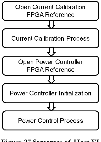
Figure 27 Structure of Host VI ... 55
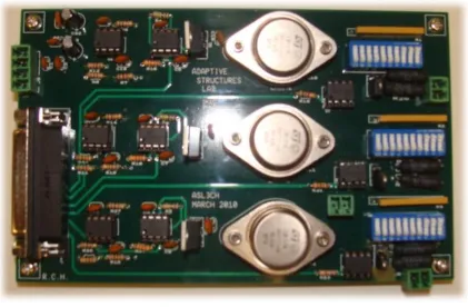
Figure 28 Electronic Hardwaee Module - PCB ... 57
Figure 29 Measurements for 0.055A Current and 0.02W Peak Power ... 60
Figure 30 Measurements for 0.055A Current and 0.05W Peak Power ... 60
Figure 31 Measurements for 0.111A Current and 0.07W Peak Power ... 61
Figure 32 Measurements for 0.111A Current and 0.2W Peak Power ... 61
Figure 33 Measurements for 0.326A Current and 0.6W Peak Power ... 62
Figure 34 Measurements for 0.326A Current and 1.6W Peak Power ... 62
Figure 35 Measurements for 0.48A Current and 1.3W Peak Power ... 63
Figure 36 Measurements for 0.48A Current and 3.5W Peak Power ... 63
Figure 37 Resistance Measurement at 0.055A ... 66
Figure 38 Resistance Measurement at 0.111A ... 66
Figure 39 Resistance Measurement at 0.326A ... 67
Figure 40 Resistance Measurement at 0.48A ... 67
Figure 41 Simultaneous Measurements from Channels 1, 2, 3 ... 70
Figure 42 Comparison of Resistance Measurements from Channels 1, 2, 3 ... 71
Figure 43 Experimental Setup for Testing an SMA Wire ... 72
Figure 44 Actuation of an SMA Wire at ~0.1W Power Amplitude ... 73
Figure 45 Actuation of an SMA Wire at ~0.2W Power Amplitude ... 74
Figure 46 Actuation of an SMA Wire at ~0.3W Power Amplitude ... 74
Figure 47 Actuation of an SMA Wire at ~0.4W Power Amplitude ... 75
Figure 48 Actuation of an SMA Wire at 0.1 Hz ... 77
Figure 49 Actuation of an SMA Wire at 0.5 Hz ... 77
Figure 50 Actuation of an SMA Wire at 1 Hz ... 78
Figure 51 Actuation of an SMA Wire at 2 Hz ... 78
Figure 52 Plot of Resistance vs Position Change, 0.4W Power Amplitude at 0.1Hz ... 79
Figure 53 Experimental Setup for Testing 6 SMA Wire Actuators ... 80
Figure 54 Actual Experimental Setup ... 81
xi
Figure 56 Plot of Resistance agains Position Change – Channels 1, 2, 3 ... 83
Figure 57 Simultaneous Actuation and Sensing of the SMA Wires - Channels 4, 5, 6 ... 84
Figure 58 Plot of Resistance against Position Change - Channels 4, 5, 6 ... 84
Figure 59 Offset Actuation and Sensing of the SMA Wires - Channels 1, 2, 3 ... 85
Figure 60 Plot of Resistance against Position Change – Channels 1, 2, 3 ... 85
Figure 61 Offset Actuation and Sensing of the SMA Wires - Channels 4,5,6 ... 86
Figure 62 Plot of Resistance against Position - Channels 4, 5, 6 ... 86
Figure 63 BATMAV – Desktop Prototype with 2 Degrees of Freedom ... 94
Figure 64 Simultaneous Actuation and Resistance Measurement from Pectoral (Blue) and Biceps (Red) muscle wires – 0.5 Hz ... 95
Figure 65 Simultaneous Actuation and Resistance Measurement from Pectoral (Blue) and Biceps (Red) Muscle Wires – 4 Hz ... 96
Figure 66 A Solid Model of Smart Inhaler System (L), A Typical Joint on the Nozzle (R) ... 97
Figure 67 Actuation of the Adaptive Nozzle Joint Actuator Wires ... 98
Figure 68 Position Tracked by the Nozzle Tip ... 98
Figure 69 Printed Circuit Board Layout ... 118
Figure 70 Important Connectors on the PCB ... 119
Figure 71 PC running LabVIEW with NI RIO device ... 120
Figure 72 Hardware Module PCB ... 121
Figure 73 DB25M Cable ... 121
Figure 74 Structure of VIs in LabVIEW ... 123
Figure 75 Current Calibration FPGA VI ... 124
Figure 76 Power Control FPGA VI ... 125
Figure 77 Power Controller Host VI – Settings Tab ... 125
Figure 78 Power Controller Host VI – Channel 1 to 3 Parameters ... 126
Figure 79 Power Controller Host VI – Channels 4 to 6 Parameters ... 127
1
Chapter 1
Introduction
1.1.
Motivation and Background
2
3
continues from the single channel prototype system developed earlier. [5] The single channel power controller used an Atmel microcontroller chip with the auxiliary electronic circuitry. The purpose of that system was to characterize electro-thermo-mechanical behavior of the SMA actuator wire.
1.2.
Review of Control Strategies used for Shape Memory Alloy Actuators
Use of SMA wires for simultaneous actuation and sensing is not a particularly new topic. Several references in the literature can be quoted that demonstrate electro-thermo-mechanical measurements from SMA wires and ad-hoc controllers to control certain mechanisms. However, a systematic account of the implementation of a power controller for SMA wires and the resistance measurement data collected in controlled conditions is hard to find. In this section, several pieces of literature have been quoted as a review of the previously completed work in this area.
Ma et. al. [10] implemented open loop control of the SMA wire actuator using pulse width modulation. Ma et. al. [11] also implemented a position control scheme with the electrical resistance of SMA using neural networks. The methodology of the actuation and sensing of the SMA actuator and its characterization is dependent on applied voltage and measured electric current through it. The authors use an HP programmable power supply in the experimental testing of the controller.
Liu et. al. [12] implemented the tracking control of SMA actuators based on self sensing feedback and inverse hysteresis compensation. The setup for the actuation and sensing uses a data acquisition and Darlington driver circuit. The characterization of the SMA actuators is done with the input voltage. A PID controller is then implemented.
Featherstone et. al. [15] described a method for improving the speed of the SMA actuators by proposing the resistance measurement as an indicator of the temperature and then controlling the rate of heating to achieve faster response. The authors termed this as a two stage relay controller.
4
Ikuta et. al. [13] implemented the resistance feedback for application in active endoscopes. Raparelli et. al. [14] measured the resistance of the SMA material under constant load.
Han et. al. [17] achieved the end point position control of a single link arm with SMA actuators. The motion of the mechanism was characterized with respect to the electric current input. The resistance feedback was not used. A Sliding mode controller was used in the application.
Several efforts have been made to utilize the resistance measurement of the SMA actuators for position control. However, a detailed account of the methodology used for the same is hard to find in the literature. Also, the resistance data collected in a controlled environment is very sparsely available.
Most researchers tend to use the input voltage or input current to characterize the behavior of the SMA material. However, these entities are only indirectly responsible for the actuation of the SMA actuators. The heating of the actuator needs to be controlled for a controlled actuation. Therefore, characterization of the SMA actuators using controlled power dissipation in it is essential. It is very hard to find the pieces of literature that document the behavior of SMA actuators under controlled power inputs.
1.3.
Scope of Research
This research focuses on developing the methodology to control the electric power dissipation in an SMA wire actuator while measuring its dynamically changing resistance. The electronic hardware, control algorithms and the software required for the same needs to be developed. Further, the method is extended for a number of SMA wires working in tandem. We call this as „multi-channel‟ implementation of the power controller system.
The prototype system needs to be validated for its functionality. This can be done using known fixed resistors. The controlled power dissipation and the resistance measurements across these resistors can be used to estimate the accuracy of the system. Further, the system needs to be tested with Shape Memory Alloy wires. FlexinolTM actuator wires produced by Dynalloy Inc.
5
1.4.
Thesis Outline
The chapter 2 of this thesis document presents an introduction to Shape Memory Alloys. The stress and temperature dependent phase transformations in these materials are explained. The chapter explains how the shape memory effect can be used for actuation purposes.
The chapter 3 presents the basics of the power control and resistance measurement methodology for an SMA wire. The functional requirements are outlined and the modular decomposition of the system to accomplish those requirements is explained. The algorithms used in this system are detailed.
The chapter 4 discusses detailed implementation of this system. The selection of each component, its functionality, operational specifications, details of software programs, flow of signals through the system is explored in depth.
The chapter 5 presents some of the results of the tests and measurements taken on this power controller system. The first part of this chapter presents results taken with known fixed resistors. In the second part, the results taken with SMA wires are presented. These results are used to validate the functionality of this system. The chapter also discusses the accuracy of measurements.
The chapter 6 discusses the specifications of this system. The safe operational ratings, absolute maximum ratings and some of the standard operation procedures are discussed.
6
Chapter 2
Shape Memory Alloys
2.1.
Background
When some metallic materials are plastically deformed, they return to their original configuration upon heating to a certain temperature. This effect is called thermal shape memory effect. In another temperature range, the same materials also exhibit a property of returning to their original configuration even after subjecting it to a strain of ~10%. This property is called as superelasticity. The two effects described above are a result of the solid to solid phase transformations that exist in these materials. These phase transformations are highly dependent on stresses and temperatures. Such materials are called as „Shape Memory Alloys‟ (SMA) or „Smart Materials‟. The thermal shape memory effect can be used to generate motion and force while the superelastic effect allows storage of energy.
Shape memory effect was first observed back in 1930‟s in Gold Cadmium alloys. [18] However, this effect received most of its attention after it was rediscovered in Nickel Titanium alloys at US Naval Ordnance Laboratory in 1960‟s. [19] Most of the research works and technical applications of SMAs are seen post 1961. The material has been known by the name Nitinol since then. (Ni-Ti for Nickel Titanium and NOL for Naval Ordnance Laboratory) Nitinol remains the mostly widely used shape memory alloy material for practical applications today.
2.2.
Phase Transformations in the SMA Material
7
When the Ni-Ti SMA material in martensite phase is heated, it starts to transform in to austenite phase. Figure 1 shows the nomenclature of various temperature values at which the transformations occur. The phase transformation from martensite to austenite starts at Austenite Start temperature (As). The transformation completes at Austenite Finish temperature (Af).
When the material is cooled, it returns back to martensite phase. However, the transformation from austenite to martensite does not occur at the same temperatures. The material starts to transform back into martensite at Martensite Start temperature (Ms). The transformation completes at Martensite Finish temperature (Mf). The temperatures at which these
transformations occur are dependent on the metallurgical properties of the material such as the composition in which Nickel and Titanium are mixed and the physical treatment that the material is subjected to.
Figure 1 Phase Transformation Hysteresis
8
austenite phase, there is a unique cubical crystal lattice structure. The austenite is also called the parent phase.
Figure 2 Geometric Changes to the Crystal Lattice Structure during Phase Transformation [20]
9
Figure 3 Phase Transformations in SMA [21]
2.2.1. Shape Memory Effect
10
is called quasiplastic behavior of SMA material. This phenomenon is shown graphically in Figure 3.
2.2.2. Superelasticity
Superelasticity is the second important phenomenon seen in the SMA materials. It is the ability of the material to return to its original shape upon unloading after a substantial deformation (~10%). The superelasticity is fundamentally seen due to the formation of stress induced martensite phase in the material. The composition of the superelastic SMA material is slightly different from the pseudoelastic material. The application of an outer stress causes martensite to form at temperatures higher than Ms. Macroscopic deformation is accommodated by the
formation of martensite. When the stress is released, the martensite transforms back into austenite and the specimen returns back to its original shape. Super-elastic SMA material can be strained several times more than ordinary metal alloys without being plastically deformed, which reflects its rubber-like behavior. It is, however, only observed over a specific temperature area. Above a particular temperature Md, the SMA can no longer form stress induced martensite. And
therefore SMA starts to deform like ordinary metals above this temperature. Also, below the temperature As, the material is martensitic and thus does not recover to austenite phase.
Therefore, the superelastic effect is only seen in a temperature range from Af to Md.
11
2.3.
Actuation using SMA
The shape memory alloys can be used to generate motion and/or force. If an SMA wire is fixed at one end, stretching it at room temperature generates an elongation after unloading. This wire remains in the stretched condition until it is transformed into austenite by heating it above the transformation temperature. The wire then shrinks to its original length. This is called free recovery of the SMA wire under no load. After cooling the wire will transform back to martensite without any macroscopic change in the shape. [22]
For actuation purposes, the constrained recovery of the SMA wire is more valuable. After stretching the wire at room temperature, the wire can be constrained by an opposing force. This force opposes the recovery of the SMA wire with heating. If this opposing force is overcome by the SMA, then it generates motion against an opposing force and hence produces work. For example, a wire suspended from a fixed support can lift a load upon heating. Upon cooling, the opposing force stretches the SMA wire back to original configuration at room temperature. Such opposing force acts as a reset force. Cyclic actuation can be effectively implemented using this phenomenon.
2.4.
Advantages and Limitations of SMA
Advantages:
There are several advantages to using SMAs for actuation purposes.
1. These actuators are small in size and have high force densities compared to conventional actuators.
2. SMAs can be used as linear actuators directly by passing electric current through them. 3. SMAs are ideal for miniaturization of systems.
4. The actuation using SMAs is silent.
Limitations:
Along with the advantages, the SMAs have their limitations.
12
2. The wide hysteresis loop and the control problems have been reported several times in the literature.
3. The actuation frequency using SMA material is limited in ambient conditions. The frequency of actuation not only depends on the heating rates but also on the cooling rates.
4. There can be fatigue effects in the material after several cycles of actuation.
2.5.
Voltage Control, Current Control and Power Control
The actuation in an SMA actuator can be brought about by heating it above a certain temperature. In order that the heating of the SMA element is uniform, a controlled heat source is needed. Heating induced by an electric current is the most convenient way. An electric current can be sent into an SMA element by applying a potential difference across it or by sending a constant current through it.
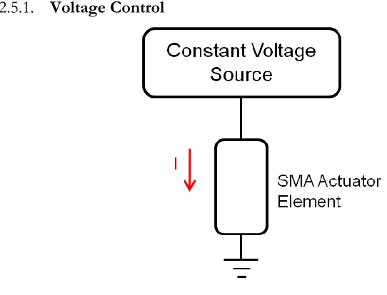
2.5.1. Voltage Control
Figure 5 Voltage Control
13
(1)
Further, as the current passes through the SMA element, it induces heat in it. This is also called „joule‟ heating. The heat energy induced in the SMA element is related to the electric power dissipated across it. The power dissipation across the SMA element is given by
(2)
The heat induced in the SMA element increases its temperature above the transformation temperature. The phase transformation takes place and the actuation stroke is obtained. However, as the phase transformation takes place and the material is strained, the resistance of the material changes significantly. [5] The change in resistance means that the flow of electric current in the wire does not remain constant as the time evolves. It also means that the power dissipated across the SMA element does not remain constant as the time evolves. As a result, the heat is not uniformly induced in the SMA element.
Further, if the strain obtained by heating the SMA element is to be controlled, then the induced heat needs to be controlled. But with a constant voltage applied across the SMA resistance, there is no way to control what the induced heat should be. In order to have some control over the heating of SMA element, the voltage delivered by the voltage source has to be controlled. This is not the most convenient way to implement the SMA actuation. Most voltage sources commercially available in the market deliver a constant voltage output or have simplistic settings for the user to pre set the output voltage value.
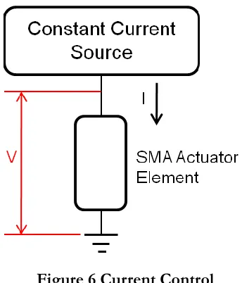
2.5.2. Current Control
Figure 6 shows an SMA actuator element connected across a source of current. When the switch is closed, the pre set current flows through the SMA element. The voltage across the SMA element is given by the Ohm‟s Law as
(3)
The current flowing through the resistive SMA element dissipates the power across it which is given by
14
Figure 6 Current Control
The heat induced in the SMA element in this case also is dependent on the electric power dissipation. The induced heat causes the temperature increase and subsequent phase transformation. The resulting actuation stroke strains the SMA element causing a change in resistance. In this case, the current source supplies a constant value of current. With the change in the resistance, the voltage across the SMA element varies. However, the power dissipation across the SMA element changes with the change in resistance. Therefore, as in the previous case, the heat induced in the SMA element varies with time.
15
Figure 7 Change in Resistance of SMA with Temperature
2.5.3. Power Control
The requirement is to achieve controlled power dissipation across the SMA element. Since this power dissipation results in a change in the resistance of SMA element, it necessitates the resistance feedback from it. It is also necessary that this power dissipation be achieved with a standard voltage or current source. This can be done using a technique called pulse width modulation. In this, the supply voltage or supply current signal is chopped into a high or on
16
Figure 8 Basics of Pulse Width Modulation
As this average power is dissipated across the SMA element, it is heated and subsequent phase transformation induces strain in it. This results, again, in a change in resistance. This resistance can be measured. The measured resistance can then be used to calculate the duty cycle of the pulse width modulated current/voltage signal so that its average value yields in the same value of power dissipated across the SMA element. So, in order to implement the PWM technique for power control, following mechanisms are necessary –
1. A voltage source or current source
2. A timing, triggering and synchronization device for generating a repetitive pulse width modulated signal
3. A switch that can be controlled by the generated pulse width modulated signal for switching the source voltage/current on or off depending on the PWM signal
4. A technique to measure the resistance
5. A computer to calculate the duty cycle based on the measured resistance and to communicate with the timing triggering and synchronization device.
The PWM technique for power control can be implemented using a constant voltage source or a constant current source.
2.5.4. Power Control using a Voltage Source
17
source and the SMA in series. There are two voltage measurements taken in this system. The first one is the voltage at the start of shunt resistor and the second one is the voltage at the start of the SMA element. The two voltages are fed to the controller. By continuously monitoring the two voltages, the current flowing through the SMA element and the duty cycle of the PWM can be computed.
Figure 9 Power Control using a Constant Voltage Source
This scheme requires a known resistor in series with the SMA element for knowing the value of the current being delivered to the SMA. The two voltage measurements are taken on either side of this resistor. The difference between the two measurements gives the voltage drop across the known value of the resistor. By Ohm‟s law, the current flowing through the series resistor can be calculated. Since the SMA element is connected in series with the shunt resistor, the current flowing through it is the same. So, the voltage measurement across the SMA
18
1. The current flowing through the SMA element does not remain constant.
2. It is necessary to monitor the instantaneous current in order to control the power. 3. The necessity of a known resistor in series with SMA causes an additional voltage drop
and loss of power
2.5.5. Power Control using a Current Source
Figure 10 Power Control using a Constant Current Source
Figure 10 shows the schematic diagram for implementing the power control using a constant current source. The constant current source ensures that the current flowing through the resistive SMA element remains constant under the specified conditions. This current can be chopped using the pulse width modulation technique. A switch is used to turn the input voltage supplied to the constant current source on or off. This switch is controlled by a PWM signal generated by the controller. The voltage measurement is taken across the SMA element and it is fed back to the controller. Since the value of the current remains constant, the voltage measurement is directly proportional to the resistance of the SMA element. The voltage measurement can then be used to calculate the duty cycle of the PWM.
19
1. If the constant current source reliably delivers a known value of current, power control is possible by simply adjusting the duty cycle.
2. Additional calculations for determining the value of current are not necessary.
3. The voltage measurement across the SMA element is directly representative of its resistance, scaled by the inverse of the constant current.
2.5.6. Selection of Power Control Scheme
20
Chapter 3
Basic Concept of Power Controller
This chapter starts with the functional requirements of the power controller system. The system is decomposed into modules and finally, an overview of the system is presented.
3.1.
Functional Requirements of the System
The power controller system is proposed to have following functional requirements -
1. Controlled power dissipation across multiple SMA wires – The first functional requirement of the power controller system is to implement a mechanism that will achieve a controlled dissipation of electric power across at least six resistive shape memory alloy wires simultaneously.
2. Resistance measurement of the SMA wires – Secondly, the system needs to have the capability to measure the resistance of the SMA wires simultaneously and continuously along with the controlled power dissipation.
3. A range of output current values – In order to actuate a variety of lengths and diameters of the SMA wires under numerous environmental conditions, a wide range of power dissipation values need to be achievable. Each value of the output current can only dissipate a certain maximum value of power in a given SMA wire, which is determined by the resistance of the wire. Therefore, a number of output current values should be achievable.
21
5. A graphical user interface for real time communication – The purpose of this system is to actuate the SMA wires implemented in novel devices to study their structural motions under controlled actuation. Therefore, it is essential for the user to communicate with the system to provide the input command power values/waveforms and to monitor the resistances of the SMA wires.
6. Modular System – It is desirable that this entire power controller system be modular. This is to easily expand the system to more number of channels if the applications demand so. It is therefore necessary that each functional block of this system be modular. A number of modules working together could then make the expansion of the power controller system possible.
3.2.
Modular Decomposition
From the list of functional requirements of the power controller system, several modules can be identified based on the functionality. These are as follows –
1. Processor – This is the module responsible for calculating the duty cycle of the pulse width modulated signal
2. PWM Generator – This module is responsible for generating the pulse width modulated signal with the same duty cycle as calculated by the processor
3. Signal Conditioning and Power Circuitry – This module uses the PWM signal to achieve a constant current signal in PWM form with the same duty cycle.
4. Calibration Circuitry – This module facilitates the automatic calibration process by changing the direction of the output PWM from SMA wire to the calibration resistors. 5. Data Acquisition System – This module measures the voltage across the SMA wire and
converts it into digital form for the processor to read it.
6. Software – The software communicates with the processor and provides it with input command power value/waveform as desired by the user and reads from it the measured voltage across the SMA wire to monitor the resistance.
22
data acquisition system can all be put together into a standard microcontroller or an FPGA based reconfigurable input output (RIO) system. The signal conditioning, power and calibration circuitry can be put together into an electronic hardware module. The software installed on a generic computer system can be the third module.
3.3.
Selection of the Modular Components
With the basic understanding of the functional requirements and the modules required to achieve those requirements, the several components can be selected.
3.3.1. Control and Data Acquisition Module
The options that need to be evaluated for this module are the several commercially available microcontrollers or the field programmable gate array (FPGA) chips along with the data acquisition systems.
The standard microcontrollers are equipped with a core microprocessor for calculations, one or more clocks, digital inputs and outputs, analog inputs and outputs, analog to digital converter (ADC), digital to analog converter (DAC), timing and triggering facilities, etc. Several digital outputs and analog inputs available on the microcontroller can be implemented for a multi channel power controller. Most microcontrollers feature only one analog to digital converter (ADC) for analog to digital conversion. Therefore, when more than one analog inputs need to be multiplexed sequentially to the ADC, the conversion from analog to digital form then takes place sequentially. In addition, all the commands are processed sequentially by the microcontroller. Therefore, the simultaneous execution of power control for several channels is not truly simultaneous. Further, there are several features provided in the microcontroller that are not useful for the application at hand.
23 3.3.2. Electronic Hardware Module
The electronic hardware module has to achieve following objectives –
1. Convert the pulse width modulated signal sent by a microcontroller or an FPGA device into a pulse width modulated constant current signal, whose constant output current value can be set by the user.
2. Create a provision for calibration mode, in which the constant output current can be calibrated as a start up procedure.
3. Send a voltage measurement across the SMA wire back to the microcontroller or FPGA for algorithmic calculations and resistance feedback.
This necessitates a constant current source that can deliver a preset value of output current. This output current then needs to be switched on or off depending upon the PWM signal generated by the controller. This can be achieved by turning the input voltage to the current source on or off. The input voltage to the current source must be from an external power supply that can source the current for all the channels of the system. So, the larger goal of power control can be achieved by turning the input voltage to the current source on or off in accordance with the pulse width modulated signal generated by the controller. A PWM controlled switch can be ideally implemented in this case which when closed connects the voltage from the external power supply to the current source. This switch can typically be a MOSFET. However, depending on the saturation voltage of the MOSFET, the PWM signal generated by the controller needs to be amplified. An operational amplifier can be used for this task.
24
A set of two switches controlled by a digital line is an ideal solution for this type of application. A PhotoMOS relay can be used.
The voltage measurement across SMA can be directly fed back to the controller using the communication cable. However, most data acquisition systems can handle only a certain maximum rated voltage. If the voltage across SMA increases beyond that limit, then the hardware gets damaged. Therefore, another operational amplifier is preferred to scale down the voltage across SMA.
The functional block diagram of the hardware module is as shown in the Figure 11.
Figure 11 Functional Blocks of Hardware Module
3.3.3. Software
25
system. The LabVIEW software needs to communicate with the controller module and the hardware module of the power controller system.
If a microcontroller is selected in the controller module, then the LabVIEW software needs a data acquisition system to communicate with it. The analog output on the data acquisition system can be used to send out the command power value / waveform. Similarly analog input can be used to monitor the voltage across SMA wire and calculate the resistance.
Instead, National Instruments have a range of Reconfigurable IO (RIO) products that feature an FPGA chip together with the data acquisition system in a single package. The FPGA chip can be programmed in the LabVIEW software itself. This saves the user from the additional programming efforts in the hardware level languages such as VHDL. The FPGA module in the LabVIEW software compiles the programs created by the user into hardware languages for the FPGA chip. Additionally, LabVIEW software on a computer can directly communicate with the FPGA chip via PCI communication bus or by USB communication.
26
At an overall system level, the National Instruments Reconfigurable IO system with integrated FPGA and data acquisition is a better option when compared to the off the shelf microcontrollers as it simplifies the overall system communication flow, gives a faster performance, delivers truly simultaneous processing for all the channels and saves the user from hardware level programming efforts.
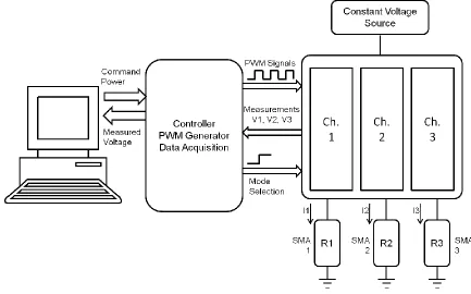
Figure 12 shows an overall schematic diagram of the multi channel power controller device.
3.4.
Concepts behind controlling power
The device delivers a pulse width modulated constant current signal to the SMA actuator wire. The value of constant current is pre-set by the user. So, the average value of current seen by the SMA actuator is given by
(5)
Where, is the duty cycle of the PWM. This electric current is responsible for joule heating of the SMA wire. Due to the constant current Iset, there is a voltage drop Vpeak across the SMA wire. This voltage varies as the resistance varies. The average power seen by the SMA wire from time
to is given by
(6) Where, is the pulsing voltage in the SMA wire. The joule heating of the SMA actuator brings about the phase transformation and an actuation stroke is obtained. Due to this phase transformation and resulting change in strain, the resistance of the SMA actuator varies significantly. The change in the resistance is captured by the peak voltage measurement across the SMA wire. The peak voltage measurement is the scaled resistance measurement in this case because the value of the set current is constant. The average power seen by the SMA wire can be further derived as follows –
27
(8)
The average power seen by the SMA can therefore be controlled if the peak voltage can be measured and the duty cycle is adjusted after a certain time interval.
3.5.
Algorithm of power control
The algorithm of power control for operation of any one channel can be summarized as follows.
At time =
1. Measure the voltage across the SMA wire.
2. This voltage is in PWM form. Therefore, what we measure is peak voltage of PWM, .
3. Read the set point power value for time from host VI, . 4. The constant current value is already stored as .
5. Using these values, the duty cycle for PWM cycle at time is given by
(9)
At time =
6. Update the duty cycle for next PWM cycle. 7. Repeat this sequence.
28
. The duty cycle for next PWM iteration is then calculated using equation (6). It should be noted that the duty cycle calculation uses peak voltage measurement of previous iteration. However, since the PWM is updated at a rate of 1 KHz, this delay of a single iteration does not significantly affect the performance of the power controller.
In addition, the host VI constantly monitors the values of the peak voltage and the duty cycle . Therefore, the instantaneous resistance of the SMA wire can be obtained as
(10)
Also, the actual tracked power in the wire can be obtained as
(11)
This value of actual power can be compared to the set point power to see the tracking effectiveness of the power controller.
3.6.
Complete Overview of the System
29
Table 1 Overview of the Multi-Channel Power Controller
Operating Principle
- Pulsed Electric Current - SMA „sees‟ average current - Controlling duty cycle controls the average power. - Section 3.4 and 3.5
Electronic Hardware Module
- Electronic Circuit that converts input PWM to PWM current signal
- Section 4.2
System Integration
- The integration of electronics with FPGA controller and LabVIEW software
30
Table 1 Continued
Algorithm
- The algorithm that runs on the FPGA controller
- Calculates the duty cycle based on voltage measurement across SMA
- Section 3.5 and 4.1.5
Standard Operational Procedures
- System Fine Tuning
- For accurate measurements and power control
31
Chapter 4
Implementation
This chapter discusses the details of the implementation of all the modules of power controller system.
4.1.
Controller Module Implementation
The National Instruments PCI-7833R card acts as the controller module of this system. This card consists of an intelligent data acquisition system with multiple digital and analog I/O lines that can be custom configured for an application specific operation with an onboard FPGA chip. The FPGA chip is user programmable using the simplistic LabVIEW block diagrams in the LabVIEW FPGA module. The program created in LabVIEW executes on the hardware which ensures direct control over all I/O signals, controlled synchronization and timing of signals, customized onboard programmed decision making with speed, reliability and parallel execution on FPGA.
4.1.1. Hardware
32
memory and it is loaded into FPGA at power on. The bus interface is used by the software to communicate with the card. The FPGA program can also be loaded from the software via bus interface.
Figure 13 Block Diagram of NI PCI-7833R [23]
4.1.2. I/O Resource Allocation
Table 2 I/O Resource Allocation
Channel PWM Out Mode Selection Signal Voltage Measurement
1 DIO1 DIO11 AI1
2 DIO2 DIO12 AI2
3 DIO3 DIO13 AI3
4 DIO4 DIO14 AI4
5 DIO5 DIO15 AI5
33
For each channel of the power controller, two digital output lines and one analog input line is necessary. For the purpose of this work, we develop a six channel power controller system. The Table 2 summarizes the allocation of the digital and analog I/O lines for the respective channels.
4.1.3. FPGA Programming
On the FPGA chip, the current calibration and the power control algorithm needs to be executed. These algorithms are discussed in section 3.5. Either of these two algorithms is selectively loaded on to the FPGA chip and executed. Both algorithms are programmed in the LabVIEW software using block diagrams. The FPGA module in the LabVIEW software is used for this purpose. The block diagram in the LabVIEW is compiled into the Hardware Device Language (HDL) and a „bitfile‟ is created. This bitfile is then transferred to the FPGA.
One of the important considerations in the FPGA programming is that it can only be programmed with integers in the LabVIEW 8.5 software. Therefore, all the logic, calculations and the decision making needs to be converted into integer format. In addition, the user also needs to make sure that the input variables sent to the FPGA chip are in integer format. Similarly, the variables monitored during the operation are also in integer format. These need to be scaled by a suitable factor to be comprehended as relevant measurements.
It is clear that in order to use the FPGA device effectively in a lab setup, another software program is necessary for higher level monitoring and control. This program is also implemented in the LabVIEW software and it is called as „host VI‟. The host VI performs several top level control tasks such as - loads the relevant program on to the FPGA chip, triggers the start of the program, sends the values of input variables in integer format, reads the output variables and converts them into the desired scale, plots the data in real time, etc. The user can therefore have complete control over the custom configured FPGA device.
34
4.1.4. Current Calibration Program on FPGA
The current calibration program is implemented as shown in the flowchart in Figure 14. The purpose of this program is to pass the current through the calibration resistor for a short period of time and measure the voltage across it. The measured voltages is then stored in a variable. This exercise is repeated for all the channels. The measured voltages are then read by the host VI. It converts these voltages to suitable scale and divides them by the known values of calibration resistors to find the current delivered by the channel.
35
Once this program loads into the FPGA, it waits for a start signal from the user controller software on the host computer. As soon as the host software sends a start signal, the program turns off the PWM generation digital outputs for all the channels (DIO 1-6). This is to make sure that initially no channel is delivering the output current signal. Then, all the mode selection digital outputs are turned on (DIO 11-16). This implies that all the channels are switched to the calibration mode. Therefore, the output current signal generated by the current source is directed to the calibration resistors. Then the program turns on the digital outputs used for the PWM generation, one channel at a time. It is to be noted that in this program, the digital outputs so not actually generate PWM. These outputs only send a high signal to their respective channel. This causes the circuitry in the hardware module to deliver a constant current signal to the calibration resistor. The FPGA then measures the voltage across this calibration resistor through the respective analog input. Since the analog inputs and the A to D conversion in the data acquisition system has an error associated with it, therefore the voltage across the calibration resistor is measured 20 times at an interval of 5µs. The ADC associated with the particular analog input converts the voltage from 10 to 10V scale to a 16 bit number between -32768 to -32768. The 20 measurements are then averaged and the average is stored in a variable on the FPGA device. When this calibration procedure is repeated for all the six channels, six values of the measured voltage across the known calibration resistors are available. The host VI then reads these variables and calculates the current delivered by each channel.
4.1.5. Power Control Program on FPGA
The power control program is executed as shown in the flowchart in Figure 15. The primary purpose of this program is to calculate the duty cycle of the PWM signal for each channel in such a way that the measured power across the SMA wire is equal to the command power set by the user. This program requires several inputs from the host VI created for the user. These are as follows –
1. Values of constant output current for all the six channels calculated using current calibration program (discussed earlier).
36
3. Value of the command power for each channel. Depending upon the form of the command power desired in the SMA wire, this value can be constant or changing with time.
Along with these inputs, the host VI also monitors the voltage measurements taken by the FPGA. The voltage measurement is used to calculate the actual measured power and the resistance of the SMA wire connected to each channel.
Once the power control program loads into the FPGA chip, it turns off all the digital outputs used for the PWM generation. This is only to make sure that no current flows through the SMA wires connected to the six channels of the system. Also, the program initializes the variables to their default values. Once the initialization is complete, the program waits until it receives a „start controller‟ command from the host VI. While the program on the FPGA is waiting for the „start controller‟ command from the host VI, it is possible for the host VI to alter the values of several variables on the FPGA chip. The host VI updates the values of channel enablers and constant output current for all the channels. After these values are updated, the host VI sends the „start controller‟ command to the FPGA.
The FPGA program then enters a loop. In this loop, the power control program repeatedly performs following tasks –
1. Generates up to six different PWM signals using six digital outputs on the data acquisition system.
2. Measures the voltages (in PWM form) across the six SMA wires connected to six channels.
a. Measures the peak voltages of the six PWM measurements from six SMA wires. b. Measures the average voltages of the six PWM measurements from six SMA
wires.
3. Uses the peak voltage measurements to calculate the duty cycles of the six PWM signals. 4. Checks if the host VI has sent a „stop controller command‟.
37
Figure 15 Power Control Program - Flowchart
38
The generation of PWM signal takes place „point by point‟ method. This means that a timed loop executes at a fixed time interval for a fixed number of iterations and sets the digital output „high‟ or „low‟ in each iteration. One point on the PWM signal gets defined as either „high‟ or „low‟ after each iteration of the loop. The time interval between the iterations and the number of iterations define the frequency of the PWM signal whereas the number of iterations in which the digital output is set to „high‟ is the duty cycle of the PWM signal. In the NI PCI-7833R card, all the digital inputs can switch between „high‟ and „low‟ as fast as 40 MHz. However, the analog inputs can only sample the voltage measurements at 200 kHz. Since the power controller application requires that the generation of PWM signal and the measurement of voltage across SMA wire be simultaneously done, the sampling rate of the analog inputs limit the PWM generation rate to 200 kHz. Since the desired frequency of the PWM signal is 1 kHz, the PWM generation loop can run 200 times at an interval of 5µs. Note that the time interval of 5µs is defined by the limiting sampling frequency 200 kHz. Sampling at a maximum of 200 kHz means that one voltage measurement can be taken at an interval no less than 5µs. Since each voltage measurement is to be coordinated with the PWM point generation, therefore each point on the PWM is generated every 5µs. Further, to achieve the desired frequency of 1 kHz, the point generation is repeated 200 times at an interval of 5 µs, making the period of the PWM signal 1ms. Figure 17 shows the LabVIEW FPGA block diagram to generate the PWM for one of the channels.
39
The code uses DIO1 for generating the PWM signal for channel 1. Throughout the PWM generation process, DIO1 is always set „true‟ by performing a logical AND operation with the channel enabler 1 variable. By performing this operation, it is made sure that the PWM is generated only if the channel is enabled by the user. It is seen that, the code generates the first point of the PWM cycle. Then there is a delay of 5µs and then a „for‟ loop executes 199 times at an interval of 5µs. This separation of the first point of the PWM from the remaining 199 points is intentionally done because the generated PWM signal is sent to the hardware module where the signal triggers the constant current through the SMA wire. The voltage across the SMA wire is then simultaneously measured in the same loop. It is seen that the measured voltage signal has a certain rise time and an overshoot before it settles down to a stable plateau. The time required for the same is experimentally observed to be ~4µs. Therefore, the first point on the PWM signal is generated outside the „for‟ loop. Inside the „for‟ loop, the generation of each point on the PWM is associated with a voltage measurement.
Figure 17 PWM Generation - LabVIEW block diagram
40
After one cycle of the PWM signal is generated and the two values of measured voltage are available, the program calculates the duty cycle for the next cycle of the PWM signal. It uses the command power value updated by the host VI, constant output current value set at the start of the program and the latest value of the measured peak voltage to calculate the duty cycle. The duty cycle is usually expressed as a percentage. However, since each PWM cycle consists of 200 points; the calculation of duty cycle in this program should yield a number between 0 and 200. This number is called „Active Points‟ in the program. Further, the voltage measurement across the SMA wire is converted by the 16 bit ADC to a number between -32768 to 32768. The FPGA program has to be written in such a way that all the calculations are performed on integers. In order to accomplish the integer math and end up with the number of active points between 0 and 199, following mathematical manipulations are made.
1. The actual voltage measurement is expressed as an integer between 32768 to 32768. -32768 and -32768 represent the full scale voltage of -10V and 10V respectively. So the ADC scales the actual measured voltage by a factor of 32768/10.
2. In the host VI, the constant output current value is multiplied by 1000 and then communicated to the FPGA. Due to this, the floating point value of the current is converted to an integer. (for example, 0.1 A becomes 100) If this scaling is not done then FPGA will round up all the current values between 0 A and 1 A to 0 A.
3. The duty cycle of the PWM is theoretically calculated using the formula
(12)
This formula yields a floating point number between 0 and 1.
4. Since the values of current and the peak voltage in the equation (12) are scaled by 1000 and 32768/10 respectively, the command power also needs to be scaled by the same factor. The host VI therefore pre-multiplies the command power value by 3276800 and then communicates it to the FPGA.
41 (13) The program calculates the number of active points for all the channels. The main power control loop then repeats. For each enabled channel, the PWM cycle is again generated using the updated value of active points.
4.1.6. Calculated Examples
This example demonstrates the calculation of the number of active points of a PWM cycle for power control application. Consider the output current of 0.1 A being passed through a resistive load of 50 ohm. The peak voltage measurement is 5 V. If the user desires to dissipate 0.4W of electric power through this resistive load, then the number of active points can be calculated by using the equation (13)
(14) Therefore, if the active or „high‟ portion of the PWM signal is 160 points or 80%, then the 0.4W of average power will be seen in the resistive load.
Now, if the user desires to dissipate 1 W of electric power through this resistive load, then the number of active points can be calculated as
(15) The number of active points to achieve 1 W power comes out to 400. However, each cycle of the PWM can only generate 200 points. Therefore, the maximum number of active points that can be achieved in the PWM signal is 200, at which the signal does not pulse anymore. It becomes a DC voltage signal. The value of number of active points therefore needs to be capped at 200 points. When the calculated number of active points exceeds 200, the PWM signal is said to be „saturated‟.
42
(16) Zero number of active points means that there will be absolutely no current signal passing through the resistive load and therefore, there will not be any power dissipated across it. However, it also means that there cannot be any voltage measurement taken across the load.
4.1.7. Limiting Values of Active Number of Points
While calculating the number of active points, it is seen that there can be two extreme situations that are undesirable for the operation of power controller system. These are –
1. The number of active points exceeds 200 2. The number of active points is 0.
In the first case, the calculation exceeds 200 when the combination of the selected output current and the resistive load reaches its maximum limit of power dissipation. If the user commands a power that is greater than the maximum limit, the number of active points exceeds 200. The maximum power dissipation limit for a selected output current and resistance is called the „saturation power‟. For all the values of command power greater than saturation power, actual measured power is the saturation power.
In the second case, when the commanded power is zero, the active number of points is also zero. This is undesirable because of there are no active points on the PWM cycle, no voltage measurement is available across the load. This results in the erroneous calculation of duty cycle and the loss of resistance measurement.
43
minimum power dissipation associate with the minimum number of active points. The value of the minimum power dissipation increases with increase in the values of minimum active points, output current and the resistance of the load. The minimum number of active points also determines the quality of mean peak voltage value. For example, if the number of minimum active points is set to 5, then, for zero command power, the value of peak voltage across the load is obtained by taking a mean of 5 measurements. For a non-zero higher command power, the number of active points can be much more than 5. Therefore, the peak voltage value is obtained by taking a mean of larger number of measurements. The difference in averaging these two values of peak voltages is reflected in the resistance measurements. It is observed that the resistance measurement is noisier when a particular channel delivers minimum number of active points in the PWM cycle as compared to the resistance measurement when the same channel is delivering a larger number of active points in the PWM cycle. This is further explained in depth in Chapter 5.
4.2.
Hardware Module Implementation
44
45
46
47
Figure 20 Probe Readouts at 5 Points on one of the channels of the Hardware Module
4.2.1. Operational Amplifier
48
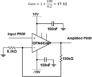
much as possible. The op amp is setup in non inverting configuration with a gain of ~15. Due to this gain, the op amp amplifies the voltage to the saturation limits.
The selection of the op amp for amplifying the PWM signal has only one main criterion. The op amp should be capable of handling supply voltages up to ±40V. Texas Instruments OPA445 is a high voltage FET-input operational amplifier that is capable of operation from power supply voltages of up to ±45V. In addition, it features high slew rate and wide power bandwidth response that is often required for high-voltage applications. TI specifies this component for typical applications in test equipment, high voltage regulators, power amplifiers, data acquisition, signal conditioning, etc. [24] The OPA445 comes in several standard packages such as TO-99, DIP-8 and SO-8. For the power controller prototype, the DIP-8 package is selected. Figure 21 shows the component block diagram and pin-outs of OPA445.
Figure 21 Operational Amplifier - OPA445 [24]
49
(17)
Figure 22 OPA445 op amp in non-inverting configuration
4.2.2. MOSFET as a Switch
The PWM signal generated by the FPGA and the amplified PWM signal by the op amp are both low current signals. These signals cannot power the SMA wire directly. These can only be used as control signals to switch a power source on or off. Therefore a switch is necessary which has a positive supply voltage at its input and the remaining circuitry at its output.
![Figure 2 Geometric Changes to the Crystal Lattice Structure during Phase Transformation [20]](https://thumb-us.123doks.com/thumbv2/123dok_us/1593330.1196532/20.612.160.459.111.312/figure-geometric-changes-crystal-lattice-structure-phase-transformation.webp)
![Figure 3 Phase Transformations in SMA [21]](https://thumb-us.123doks.com/thumbv2/123dok_us/1593330.1196532/21.612.94.527.77.286/figure-phase-transformations-in-sma.webp)