Design and Simulation of Solid State Power
Amplifier using GaN Devices
Madhumita M Dhara, Dr. S.K. Chhotaray
ME Student, Dept. of E&C, Sardar Vallabhbhai Patel Institute of Technology, Vasad, Gujarat, India Asst. Professor, Dept. of E&C, Sardar Vallabhbhai Patel Institute of Technology, Vasad, Gujarat, India
ABSTRACT: This paper proposes the design of Solid State Power Amplifier (SSPA) using ADS (Advanced Design System). Here GaN device is used for the design of high power amplifier as the recent era is for achieving the high RF power. GaN devices proves better gain and power than GaAs devices. The various steps involved for the present design are Direct current (DC) simulation for getting the proper quiescient operating point. Also, Stability simulations is to be carried to check the unconditional stablility of the amplifier. Load Pull technique is then carried out to match the load impedances, and finally Harmonic Balance (HB) simulation to verify the harmonic levels of signal other than designed frequency of operation.
KEYWORDS: Solid State Power Amplifier (SSPA), Power Amplifier (PA), Advanced Design System (ADS), Gallium Nitride (GaN), Direct Current (DC), Harmonic Balance (HB), Load-Pull technique, Power Added Efficiency (PAE
).
I. INTRODUCTION
A power amplifier in a communication transponder along with transmitter antenna decides the Effective Isotropic Radiated Power (EIRP) of the satellite. Now-a-days a higher EIRP is asked for due to the increasing requirement of higher channel capacity and better coverage. Gain of the transmit antenna is proportional to its size and so larger antennas cannot be accommodated on the payload. Therefore, in meeting the EIRP requirement of satellite power amplifier plays an important role.
This paper presents the work done on simulation and optimization of a 45 Watt, 1.5 GHz power stage based on GaN device. The non-linear model of the device is used in ADS to design the power stage, including bias network design, stability analysis, load-pull technique. With 73% efficiency, 47.7dBm output power and 11dB gain is achieved through load-pull technique. This paper describes the process of designing a single stage class-AB PA for the operation in 1.5 GHz frequency amplifiers and high power amplifiers. Due to the advantages of SSPA over TWTA here we are going to design a Solid State Power Amplifier.
Important considerations for RF and microwave power amplifiers are efficiency, gain, linearity (intermodulation products) and thermal effects [2], [3]. Linearity and efficiency are the contradictory requirements
This paper is organized as follows. Section II contains existed system III classification of Solid State Power Amplifier, section IV explains class AB power amplifier, section V explains load-pull technique, section VI describes the design process and simulation. Finally, the conclusion is specified in section VII.
II. RELATED WORK
voltages [1]. For lower power applications SSPAs are preferred than TWTAs because of their simplicity and smaller size [1]. Also, the mean time between the failures is low in TWTAs.
SSPAs consists of small signal amplifiers, medium poweramplifiers and high power amplifiers. Due to the advantages of SSPA over TWTA here we are going to design a Solid State Power Amplifier. Important considerations for RF and microwave power amplifiers are efficiency, gain, linearity (intermodulation products) and thermal effects [2], [3]. Linearity and efficiency are the contradictory requirements.
III.CLASSIFICATION OF SOLID STATE POWER AMPLIFIER
SSPA is an amplifier that uses transistors (BJT or FET) to provide useful amplification at different frequency levels (MHz or GHz range).
The Solid State Power Amplifier is classified into different classes of operation depending on the operating frequency or bias point of the circuit. The main categories of power amplifier are: linear and non-linear amplifiers. Linear amplifiers preserve the waveform shape of the input signal at the output while the Non-Linear amplifiers has the inevitable distortion in the signals and are suitable for constant envelope signals. Amplifier classes have unique bias level for their objectives and has their own trade-offs [4]. The most common linear amplifier classes are A, B, AB; while class A being the most linear of all amplifier types. The main Non-Linear amplifier classes are C, D, E, F, G, H and S [5]. Based on where the device is biased and if the device is operated as switch, there are broadband linear amplifiers such as class A, AB, B.
In this paper we are going to design a class AB amplifier which has a higher efficiency than class A and it reduces the crossover distortion, present in class B. Here the main parameter for the design of an amplifier is higher efficiency and high output power so class AB is more preferred. There is a compromise between the linearity and efficiency.
IV.CLASS ABPOWER AMPLIFIER
Class AB is a linear amplifier and is a compromise between Class A and Class B regarding to efficiency and linearity parameters. It operates between the two edges of class B and class A amplifiers. In the ideal case, an operating class ABmode is biased to a quiescient point, which stands in a region between the cut-off point and bias point of class A. The efficiency is less than 78.5% which is improved than class A PA. The conduction angle in this class is between 180˚ and 360˚. Class AB utilize wider dynamic range than the two linear PA discussed.
The Non- Linear effects refer to the distortion of the signal waveform. Power amplifiers are operated at or beyond 1 dB compression point, cut-off and the clipping behavior of the transistor become stronger, hence the transistor become more non-linear. Two types of matching techniques are: Conjugate matched and Power matched. Power match technique extracts maximum power from the device.
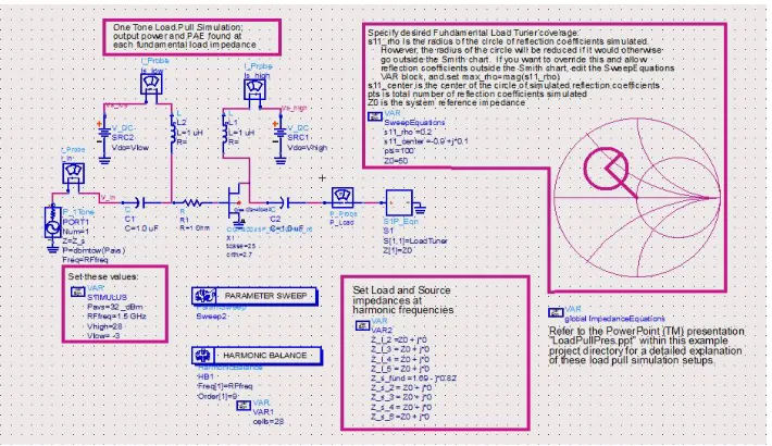
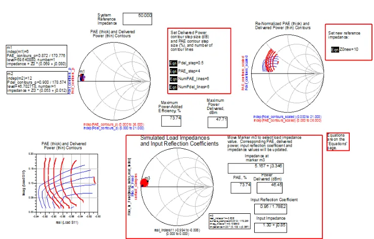
Load- Pull technique does the job of finding a suitable power match for the device [2], [6], [7]. The input is fixed and the load is varied so to find an optimum termination. The parameters of interest are delivered power, power added efficiency (PAE) and IMD figure. As load termination is varied the measure of these parameters is tabulated. Contours of delivered power, PAE and IMD are then plotted on Smith Chart.
VI.PROPOSED METHODOLOGY
The transistor used in this design is CGH40045 with the design frequency of 1.5 GHz. Design process will be followed in the below mentioned steps:
A. DC and Loadline Analysis B. Stability Analysis
C. Load-Pull Analysis
D. Harmonic Balance Analysis
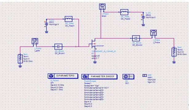
A. Direct Current (DC) and Loadline Analysis:
The device has to be biased such that it gives maximum output power without clipping the input signal. The range of the output or current signal should not be limited by the device if it has to perform in the linear region [2], [4]. Drain current vs Drain voltage is plotted in ADS for different value of gate voltage Fig. 5
`
Fig. 2. Bias supply schematic in ADS
B. Stability Analysis
It is necessary to check the stability of the device even beyond the operating frequency range to check the undesired potential
Fig. 3. Amplifier schematic with stability network
C. Load-Pull Analysis
Load Pull technique is used to find the power match for the device. ADS provides an built-in load-pull simulatorcircuit. It provides an equation based S-parameter block which can provide different values of reflection coefficient.This S-parameter block is used as load tuner. An optimum load which can provide desired output power and poweradded efficiency is then found out. These values can then be used to draw the contours using in built function in ADS[7]. The schematic of load pull technique for single tone is shown in fig. 4. The simulated load reflection coefficient,
output power and PAE is shown in fig. 7.
D. Harmonic Balance Simulation
Harmonic balance simulation calculates the response of large signal circuits driven by single or multiple sources and it tries to find a stationary solution for the non-linear system in the frequency domain. As two signals are mixed different intermodulation terms are generated. To check the IMD performance load pull technique for two tone signalis done. As the device is operated in more non-linear region IMD gets poorer. Fig.8 shows the 3rd order IMD products in harmonic balance two tone test.
VII.SIMULATION AND RESULTS
Fig. 5. Drain current vs Drain voltage Fig. 6. Mu1 and stability factor for stable networ
Fig. 7. Resulting PAE and delivered power contours drawn in Smith chart
10 20 30 40 50
0 60
0 5 10 15
-5 20
VGS=-3.000 VGS=-2.500 VGS=-2.000 VGS=-1.500 VGS=-1.000 VGS=-0.500 VGS=0.000
VDS
ID
S
.i
,
Fig.8. Harmonic Balance Two-Tone Test
VIII.CONCLUSION AND FUTURE WORK
This paper proposes the design of Solid State Power Amplifier for satellite applications using ADS software. Here bias point and stability is initially checked and the desired output power and PAE is achieved using load-pull technique. In future this design can be extended for achieving higher efficiency using class F operation.
REFERENCES
1. K. S. Parikh. “Communication Transponders" in IITP ASIM-Applications Area Module, Ahmedabad: Space Applications Area, ISRO, 2010, pp. 37-52s
2. Steve C. Cripps, RF Power Amplifiers for Wireless Communications, Boston: Artech House, pp. 1-24,2006
3. D. M. Pozar, Microwave Engineering, New Delhi: Wiley India, pp. 522-555,540-555,570-573, 2007
4. Cotter W. Sayre, Complete Wireless Design. McGraw-Hill, inc., 2001
5. Peter B. Keningto, High-Linearity RF Amplifier Design. Artech House, inc., 2000
6. John Olah and Sanjeev Gupta, Power Amplifier Design Using Measured Load Pull Data, Microwave Engineering Europe, pp. 23-30, 2003
7. Andy Howard, Making Power Amplifier Design Easier with Custom Templates, Internet: www.home.agilent.com
8. Adel S. Sedra and Kenneth C. Smith, Microelectronic Circuits, New York: Oxford University Press, pp. 236-242, 415-418, 2004
9. Using Advanced Design System to Design an MMIC Amplifier, Agilent EEs of EDA Application Note Number 1462
10. Jan M. Weekley and Bill J. Mangus, “TWTA Versus SSPA: A Comparison of On-Orbit Reliability Data”, Vacuum Electronics Conference, 2004. IVEC 2004.
Fifth IEEE International, pp. : 650-652, 2005
11. Masaaki Kuzuhara, “GaN-based electronics”, The Ninth International Conference on Advanced Semiconductor Devices and Microsystems, IEEE, pp.: 1-6, 2012.
12. Karim Boutros, Rongming Chu, Brian Hughes, “Recent Advances in GaN Power Electronics”, Custom Integrated Circuits Conference (CICC) IEEE, pp.:1-4,
2013
BIOGRAPHY
Madhumita M. Dharais anM.E. student in the Electronics & Communication Department, SardarVallabhbhai Patel Institute of Technology, Vasad, Gujarat, India. She received degree of B.E.inElectronics & Communication in 2013 fromB.H. Gardi College of Engg. & Tech., Rajkot, Gujarat, India. Her areas of interest are microwave engineering wireless communication system, digital electronics.