Effect of InGaN thickness on assisted trap recombination
and behaviour of InGaN/AlGaN double heterostructure LED
Shanise Rashid1,*, M.Halim A. Wahid1, N. Azura M. Ahmad Hambali1, N.Syafira Abdul Halim1, and Mukhzeer M.Shahimin21Semiconductor Photonics & Integrated Lightwave Systems (SPILS), School of Microelectronic Engineering, Universiti Malaysia Perlis, Pauh Putra Campus, 02600 Malaysia.
2Department of Electrical and Electronic Engineering, Faculty of Engineering, National Defence University of Malaysia (UPNM), Kem Sungai Besi, 57000 Kuala Lumpur.
Abstract. This work is dedicated to the study of InGaN based LED on the thickness variation effect. The operating voltage, total emission rate, efficiency droop and spontaneous recombination rate was improved by increasing the thickness of InGaN layer of InGaN/AlGaN electron blocking layer (EBL). Based on optical and electrical results, the thicker InGaN layer could have lower operating voltage and higher total emission rate. LED with 5nm thick InGaN layer also could prevent electron leakage into p-region and improve hole injection efficiency. As a result it decreases 60% of efficiency droops and reduces the trap assisted recombination in InGaN/AlGaN active light emitting region. This indicates that InGaN layer may decrease the non-radiative recombination.
1 Introduction
Nitrides semiconductors, especially the gallium nitride (GaN) based light emitting diode (LED) with an InGaN/AlGaN double heterostructure, are among the most promising optoelectronic devices to be developed in recent years [1-3]. With wide bandgap of GaN, thus will emit light from close to the UV range to blue, it can be used in various lighting devices with colour converting material [4]. Recent works based on microsphere array [5,6] and photonic crystal [7] showing great potential to enhance the light extraction efficiency (LEE) in GaN based LEDs. Although the output power of current LEDs is already high, the output efficiency of these LEDs is still required further improvement to achieve feasible solid state lighting (SSL). Besides that, the carrier injection efficiency has the key functions in the light emission efficiency of GaN based LEDs. Meeyard et al. [8, 9] reported asymmetry during carrier transport because of the much lower concentration and mobility of holes in p-GaN and p-AlGaN compared with electrons. The asymmetry in carrier transport reduces the light emission efficiency of LEDs and enlarges the efficiency droop.
Recently, it has been suggested to redesign the electron blocking layer (EBL) because it can lead to weak electron confinement and can act as a potential barrier for holes injection [10]. Yu et al. [3]
experimentally and theoretically showed that EBL with thick InGaN layer have improved hole injection efficiency and increasing emission properties.
In this study, we investigate the thickness effect of InGaN layer on optical and electrical properties of the active light emitting region of InGaN/AlGaN LEDs.
2
Methodology
The active double heterojunction region, from which the desired emitted light, is modelled stand on the very basis of the GaN based blue LED structure that once has been fabricated by Nakamura et al. [11]. This device consists of p-GaN layer, an active region of 0.15µm thickness of Al0.15Ga0.85N layer and 2nm thickness of In0.06Ga0.94N
layer. Note that only the active light emitting region of GaN based blue LED is modelled. The lower AlGaN layer is n-doped while the upper AlGaN layer is p-doped. The InGaN layer is undoped, thus creates PIN diode structure with the light emitting InGaN layer in the central intrinsic region. The device geometry has lateral dimension of 200x200 µm which is a standard size of LED device. The structure of the LED device is shown in Figure 1.
factor for electrons and holes = 1.7x10⁻³⁰ cm6s-1) and
carrier lifetimes for trap assisted recombination (electron and hole lifetime = 1x10⁸ s) have been included in the
materials [12-13]. All the parameters are based on GaN properties from semiconductor module material library but values of electron affinity and bandgap energy have been altered to reflect In and Al alloy composition. Quantum confinement effect is not included within the thin InGaN material in this model. This is because quantum dots take many geometries, thus Schrodinger equation has to be solved which is not the interest of the study at the moment, hence it will take longer computation time.
In order to apply voltage and current bias to the device, metal contact boundary conditions are applied to the bounds of geometry as illustrated in Figure 1(a). This is to enable toggling between thermionic emission heterojunction continuity model and continuous quasi-Fermi levels.
(a)(b)
Fig. 1. Geometry of LED device. (a) Structure of modelled layers. The focused section is highlighted in red line. (b) Double heterostructure region of full device in 1D model.
The AlGaN thickness and Al% in InGaN/AlGaN EBL is fixed at 0.15µm and 15%, respectively. The InGaN In% in InGaN/AlGaN is fixed at 6%. The InGaN thickness in InGaN/AlGaN EBL for 2nm is set as reference LED (ref-LED) and others are variably set at
reduction of trap assisted recombination in the active region. Only the thicknesses have been varied while other parameters that can affect the simulation such as bandgap and value of electron affinity of InGaN and AlGaN are fixed as summarized in Table 1.
Table 1. Material properties. Property Unit, V Bandgap of AlGaN 3.7 Bandgap of InGaN 2.8 Electron affinity of AlGaN 4.1 Electron affinity of InGaN 4.6
Three investigations are performed in this work which are preliminary mode, voltage biased and current biased studies. Preliminary study is used to connect the doping and transition level from the continuous quasi-Fermi level heterojunction continuity model to suitable level of thermionic emission model. Then, voltage sweep is used to apply bias voltage ranges from 0V to 3.3V across the device. Current injection study is adopted to converge initial solution from voltage driven and to sweep several orders of magnitude of 1µA to 700 µA through the device.
3
Results and discussion
Figure 2 shows the forward current-voltage (I-V) characteristic curves of all fabricated LEDs with different thicknesses of InGaN layer. Forward voltage (Vf) of ref-LED is 3.19V while LEDs I to III are 3.186V, 3.183V and 3.182V respectively. The Vf of LEDs I, II and III are lower than ref-LED is recorded. This reduction might be due to the decrement of effective potential barrier on the hole carrier between p-GaN and p-AlGaN/InGaN active double heterojunction region.
Fig. 2. I-V characteristics of all LEDs.
n-AlGaN p-AlGaN
emission rate from InGaN layer as a function of applied current. The visible effect is known as LED droop. This LED droop caused by a non-radiative carrier loss mechanism that has little effect at low currents, but become dominant at high currents. In general, carrier losses can occur either inside or outside the active region. The results show that the total emission rate of InGaN layer increases with thickness. At 100mA, LED III shows the highest total emission rate, 1.2x10¹⁷ (s-1) follows by LED II and LED I, 1.12x10¹⁷ (s-1) and 1.03x10¹⁷ (s-1) respectively. Ref-LED demonstrates the lowest total emission rate of 1x10¹⁷ (s-1).
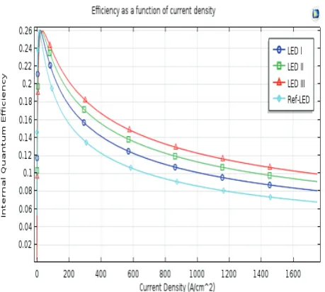
The efficiency droop is even more apparent in Figure 4 which portrays the internal quantum efficiency (IQE) as a function of current density. Not all electron hole recombination is radiative. IQE is the proportion of all electron-hole recombination in the active region that are radiative, producing photons. There is a peak in the IQE at current density around 30 (A/cm-2) with applied current in the 10-30mA range and there is rapid drop off for densities in access 100 (A/cm-2). The IQEs for all LEDs are almost the same at low current density. However, when the current increases to 1600 (A/cm2), the efficiency droop appears and the difference is clearly visible. It is also observed that the IQE of ref-LED decreases almost 73% when the current increases to 1600 (A/cm2), while IQE for LED I decreases by 63%, follows by LED II 64% and LED III decreases only 60%. This demonstrates that the structure with thicker InGaN layer can improve the efficiency droop significantly, which suggests that the proposed thickness of InGaN layer can mitigate the problem of injection current efficiently.
Fig. 3. Total emission rate as a function of current of all LEDs. The sublinear curve is a characteristic of LED droop.
Fig. 4. Efficiency as a function of current density of all LEDs.
Based on droop efficiency that increases with thickness of InGaN layer, this indicates that InGaN layer may decrease the non-radiative recombination. Non-radiative recombination consists of Shockley Read Hall (SRH) or called as trap-assisted recombination process and Auger recombination process. Auger recombination is smaller than SRH recombination which is constant
with Kuo’s result that the Auger recombination can be
ignored under the case that the carrier density is below 1x1020 cm-3 [14]. Semiconductor diode would deviate from ideal behaviour when generated-recombination processes took place in the depletion region as described by Shockley [15]. It is confirmed that SRH generated- recombination in the depletion region could control the feature of semiconductor diodes. The performance of LED is further explored to support those theories.
(b) 3nm thickness of InGaN layer
(c) 4nm thickness of InGaN layer
(d) 5nm thickness of InGaN LED
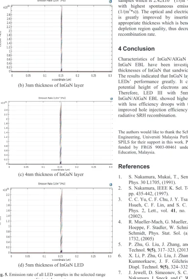
Fig. 5. Emission rate of all LED samples in the selected range of injected currents.
Figure 5 depicts the emission rate in the active region of LEDs with different InGaN thicknesses. The emission from InGaN layer in all samples is significantly larger than in the cladding material due to InGaN layer is the only region of the device which has a high concentration of both holes and electrons. The results
samples which is 2.42x1033 (1/(m3*s)) compared to 2nm with highest spontaneous emission rate, 4.01x1033 (1/(m3*s)). The optical and electrical behaviour of LED is greatly improved by inserting InGaN layer of appropriate thickness which is beneficial to improve the depletion region quality, thus decreases the spontaneous recombination rate.
4
Conclusion
Characteristics of InGaN/AlGaN LED with undoped InGaN EBL have been investigated with different thicknesses of InGaN that sandwiched between AlGaN. The results indicated that InGaN layer thickness affected
LEDs’ performance greatly. It changes the effective potential height of electrons and holes respectively. Therefore, LED III with 5nm InGaN layer of InGaN/AlGaN EBL showed highest total emission rate with less efficiency droops with the injection current, improved hole injection efficiency and reduce the non-radiative SRH recombination.
The authors would like to thank the School of Microelectronics Engineering, Universiti Malaysia Perlis (UniMAP) especially SPILS for their support in this work. Partial of this research is funded by FRGS 9003-00461 under Ministry of Higher Education, Malaysia.
References
1. S. Nakamura, Mukai, T., Senoh, M., Jpn. J. Appl. Phys. 30 L1705, (1991).
2. S. Nakamura, IEEE K. Sel. Topics ., vol. 3, no. 2, pp. 435-442, (1997).
3. C. C. Yu, C. F. Chu, J. Y. Tsai, H. W. Huang, T. H. Hsueh, C. F. Lin, and S. C. Wang, Jpn. J. Appl. Phys. 2, Lett., vol. 41, no. 8B, pp. L910–L912, (2002).
4. R. Mueller-Mach, G. Mueller, M. R. Krames, H. A. Hoeppe, F. Stadler, W. Schnick, T. Juestel, and P. Schmidt, Phys. Stat. Sol. (a) 202, No. 9, 1727-1732, (2005)
5. P. Zhu, G. Liu, J. Zhang, and N. Tansu, J. Displ. Technol. 9(5), 317–323, (2013).
6. X. Li, P. Zhu, G. Liu, J. Zhang, R. Song, Y. Ee, P. Kumnorkaew, J. F. Gilchrist, and N. Tansu, J. Displ. Technol. 9(5), 324–332 (2013).
7. J. Jewell, D. Simeonov, S. C. Huang, Y. L. Hu, S. Nakamura, J. Speck, and C. Weisbuch, Appl. Phys. Lett. 100(17), 171105, (2012).
8. D. S. Meyaard, G.-B. Lin, Q. Shan, J. H. Cho, E. F. Schubert, H. Shim, M. H. Kim, and C. Sone, Appl. Phys. Lett. 99(25), 251115, (2011).
11. S. Nakamura,T. Mukia, and M. Senoh, Appl. Phys. Lett. 64, 1687, (1994).
12. Y.C. Shen, G. O. Mueller, S. Watanabe, N. F. Gardner, A. Munkholm, and M. R. Krames, Appl. Phys. Lett. 91, 141101 (2007).
13. Q. Dai et al., Appl. Phys. Lett. 94, 111109, (2009). 14. S. H. Yen, M. C. Tsai, M. L. Tsai, Y. J. Shen, T. C.
Hsu, and Y. K. Kuo, Appl. Phys., A Mater. Sci. Process. 97(3), 705–708 (2009).