© 2015, IRJET ISO 9001:2008 Certified Journal Page 2024
Closed loop control of an Improved Dual switch Converter With
Passive Lossless Clamping For High Step-Up Voltage Gain
Sonima Gabrial C.G
1, Roshima T V
21 PG Scholar, Dept. of EEE, Jyothi Engineering College, Thrissur, India
2Assistant Professor , Dept. of EEE, Calicut University, Jyothi Engineering College, Thrissur, India
---***---Abstract—The conventional dc-dc boost converters
are unable to provide high step up voltage gain. The transformer less dc-dc converters are used to achieve high step up voltage gain without an extremely large duty ratio. The improved dual switch converter can achieve high voltage gain with a condition that the parameters are inconsistent. It has advantages of low voltage and current stress on the switches compared to the transformer less dc-dc converters. The proposed converter also provides the solution to balance the voltage on the switches and to suppress the resonance. This is possible due to the presence of passive lossless clamping. With the passive lossless clamping circuits, low voltage switches with small Rds (on) can be utilized, and hence the efficiency of the converter can be increased. The simulation of the circuit with 30 V input, 100V/1A output is done using MATLAB.
Keywords—highstep-upvoltagegain, passivelossless clamping, parameters are inconsistent,resonance.
Introduction
The voltage conversion ratio of a traditional boost converter is limited. various technologies have been developed to provide a high step-up voltage gain. The traditional boost converter is hard to provide a large voltage conversion ratio. A large duty cycle is introduced that brings high conduction loss, and the peak current may impact the capacitors. The isolated converters will boost the voltage by increasing the turns ratio of the high frequency transformers. By using the multistage dc to ac to dc power conversion, the cost is increased because many isolated sensors and feedback controllers are required. But the main limitation of the leakage inductance should be handled carefully or it may cause high voltage spikes. The coupled inductors can serve as a transformer that is used to enlarge the voltage gain in transformer less dc/dc converters. By increasing the turns ratio, high voltage gain can be easily achieved but the leakage inductance of the coupled inductors is inevitable. It may also cause high voltage spike, which will increase the voltage stress. The switched inductor boost converter can provide a high
voltage conversion ratio, but the voltage stress on the power switches is relatively high. The switched capacitor boost converter can provide a high voltage conversion ratio, whereas multiple diode-capacitor units are utilized with low power density. The cascade boost converter can provide a high step-up voltage, whereas this topology is complicated and the efficiency may deteriorate with a multistage structure. The transformer less dual-switch converter has inherent high step-up characteristic with low voltage and current stress on the power switches. This converter is composed of two inductors and two switches sharing the same operation signals. This topology is very simple,and the voltage and current stress on the power switches is low compared with that on the boost converter. One of the main peculiarity of the transformer less dual-switch converter with passive lossless clamping is that its consistency. Else, the inductors and parasitic capacitors will constitute resonance circuit, which induces increased voltage stress and reduced efficiency. Passive lossless clamping is adopted to balance the voltage across the switches and to suppress the resonance. With the passive lossless clamping circuits, low voltage switches can be utilized, and the efficiency of the converter can be improved. Compared with the two stage boost converter, it has the same amount of power switches and passive components. However the converter has the advantages of the voltage stress across power devices is relatively low compared to the secondary stage of the two-stage boost converter and the system stability of the cascade structure is another issue which can be avoided. The voltage conversion ratio remains high, thus making the converter more suitable for step up dc-dc power conversion. The converter is simulated using MATLAB. Output levels are obtained as per the design values for both converter operations. Simulation results conveys the operability of the dual switch converter with passive lossless clamping structure.
LITERATURE SURVEY
© 2015, IRJET ISO 9001:2008 Certified Journal Page 2025 intensity-discharge lamp ballasts for automobile
headlamps. Theoretically, a dc–dc boost converter can achieve a high step up voltage gain with an extremely high duty ratio [1]–[3].However, in practice, the step-up voltage gain is limited due to the effect of power switches, rectifier diodes, and the equivalent series resistance (ESR) of inductors and capacitors.
The conventional boost converter is used to provide a voltage conversion ratio with low voltage gain. It is hard to provide a large voltage conversion ratio, due to a large duty cycle that brings high conduction loss, and the large peak current may impact the capacitors seriously. Various topologies have been developed to provide a high step up voltage gain without an large duty ratio [4]. The isolated converters will boost the voltage by increasing the turns ratio of the high frequency transformer [5]-[6]. However, it may cause increased weight, volume, high switching losses, high electromagnetic interference. And also the leakage inductance should be carefully handled [7]-[9]. Otherwise, there will be a voltage spike across the power switches. The transformer less dc/dc converters are used instead of the isolated converters. The coupled inductors are used to achieve high voltage gain in the transformer less dc/dc converters. By increasing the turn’s ratio, high voltage can be easily achieved [10]-[13]. Unfortunately, the leakage inductance of the coupled inductors is also inevitable. And also it may cause high voltage spike, that will increase the voltage stress [14],[15].
The non coupled inductor type transformer less converters are used such as the switched-capacitor-inductor converters. A small resonant switched-capacitor-inductor is used in these converters to limit the current peak caused by the switched capacitors. Here the voltage stress on the switch is smaller than the voltage stress on the switch in conventional boost converter [16]-[18]. The switched inductor multilevel boost converter [19]-[21] is having a single stage dc-dc boost converter topology with very large voltage conversion ratio based on the pwm technique. A high switching frequency is employed to decrease the
size of these components. But the voltage stress on power switches are relatively high. The switched capacitor boost converter [22]-[24] can provide a high voltage conversion ratio, where as the multiple diode-capacitor units are utilized with low power density. The cascade boost converter can provide a high step-up voltage, where as this topology is complicated and the efficiency may deteriorate with a multistage structure.
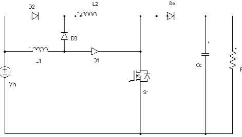
[image:2.595.310.546.420.554.2]Many topologies have been presented to provide a high step-up voltage gain without an extremely high duty ratio [25]-[26]. A dc-dc fly back converter is a very simple structure with a high step-up voltage gain and an electrical isolation, but the active switch of this converter will suffer a high voltage stress due to the leakage inductance of the transformer. Transformer less dc-dc converters, which include the cascade boost type [27] which are complex and having a higher cost. The modified boost type with switched inductor technique is shown in Fig.1 [28]
Fig. 1. Modified boost type with switched inductor technique
© 2015, IRJET ISO 9001:2008 Certified Journal Page 2026 power device exists in the current-flow path during
the switch off period. 2) The voltage stresses on the active switches are less than the output voltage; and 3) under the same operating conditions, including input voltage, output voltage, and output power, the current stress on the active switch during the switch-on period is equal to half of the current stress switch-on the active switch of the converter in [28]. The transformer less dual switch converter has an inherent high step-up characteristic with low voltage and current stress on the power switches [29]. However, the converter has very strict requirement of the device parameters consistency. Otherwise, the inductors and capacitors will constitute the resonance circuit, which induces increased voltage stress and reduced efficiency.
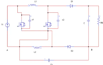
[image:3.595.320.539.275.413.2]The improved dual switch converter with passive lossless clamping for high step-up voltage gain is works on the principle of device inconsistency. In the practical conditions the two inductors, the two parasitic capacitors and the switching speed of the two power switches are not exactly equal. Passive lossless clamping is adopted to balance the voltage across the switches and to suppress the resonance.
Fig.2 A transformer less dc-dc high step up converter
Fig. 3. Shows the Circuit configuration of the improved dual switch converter with passive lossless clamping for high step-up voltage gain. Switches S1 and S2 share the same operation signals; when the switches are turned on simultaneously, inductors L1 and L2 are parallel connected; and when S1 and S2 are turned off, L1 and L2 are series connected. The figure shows the solutions to suppress the resonance by dividing the original output diode D into two diodes D1 and D2, and a capacitor Cc is added to clamp the switches.
Fig. 3: Circuit configuration of the improved dual switch converter with passive lossless clamping for high step-up
voltage gain
The voltage conversion ratio of the conventional boost converter is D/1-D whereas the voltage conversion ratio of the improved dual switch converter with high step-up voltage gain is 1+D/1-D. And also the voltage stress across the switches are half as compared to the transformer less dual switch converter. In order to simplify the design procedure, all the parameters are designed in the ideal conditions, and the switching transition time is too short and can be omitted.
SIMULATION RESULTS
[image:3.595.59.259.507.646.2]© 2015, IRJET ISO 9001:2008 Certified Journal Page 2027
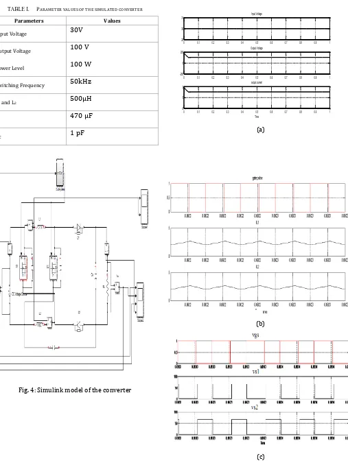
TABLE I. PARAMETER VALUES OF THE SIMULATED CONVERTER
Parameters Values
Input Voltage 30V
Output Voltage 100 V
Power Level 100 W
Switching Frequency 50kHz
L1 and L2 500µH
C 470 µF
[image:4.595.40.268.112.638.2]Cc 1 pF
Fig. 4: Simulink model of the converter
0 0.1 0.2 0.3 0.4 0.5 0.6 0.7 0.8 0.9 1
29 30 31
Input Voltage
0 0.1 0.2 0.3 0.4 0.5 0.6 0.7 0.8 0.9 1
-200 0 200
Output Voltage
0 0.1 0.2 0.3 0.4 0.5 0.6 0.7 0.8 0.9 1
-2 0 2
Time output current
(a)
(b)
© 2015, IRJET ISO 9001:2008 Certified Journal Page 2028
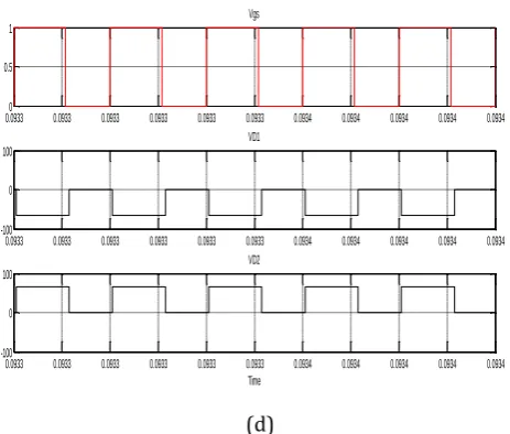
0.09330 0.0933 0.0933 0.0933 0.0933 0.0933 0.0934 0.0934 0.0934 0.0934 0.0934 0.5
1
Vgs
0.0933 0.0933 0.0933 0.0933 0.0933 0.0933 0.0934 0.0934 0.0934 0.0934 0.0934 -100
0 100
VD1
[image:5.595.44.276.106.303.2]0.0933 0.0933 0.0933 0.0933 0.0933 0.0933 0.0934 0.0934 0.0934 0.0934 0.0934 -100 0 100 Time VD2 (d)
Fig. 5: Simulated key waveforms of the converter
0 0.1 0.2 0.3 0.4 0.5 0.6 0.7 0.8 0.9 1
29 29.5 30 30.5 31 i n p u t v o l t a g e
0 0.1 0.2 0.3 0.4 0.5 0.6 0.7 0.8 0.9 1
-50 0 50 100 150 Time o u t p u t v o l t a g e , o u t p u t c u r r e n t
Fig. 6: Load regulation of the converter
0 0.1 0.2 0.3 0.4 0.5 0.6 0.7 0.8 0.9 1 29 30 31 in p u t v o lt a g e
0 0.1 0.2 0.3 0.4 0.5 0.6 0.7 0.8 0.9 1 -100 0 100 200 o u t p u t v o lt a g e
0 0.1 0.2 0.3 0.4 0.5 0.6 0.7 0.8 0.9 1 -1 0 1 2 Time o u y p u t c u r r e n t (a)
0 0.1 0.2 0.3 0.4 0.5 0.6 0.7 0.8 0.9 1
39 40 41 in p u t v o lt a g e
0 0.1 0.2 0.3 0.4 0.5 0.6 0.7 0.8 0.9 1
-100 0 100 200 o u t p u t v o lt a g e
0 0.1 0.2 0.3 0.4 0.5 0.6 0.7 0.8 0.9 1
[image:5.595.309.557.110.295.2]-1 0 1 2 Time o u t p u t c u r r e n t (b)
Fig . 7: Line regulation of the converter at (a)Vin = 30 V (b) Vin = 40V
Fig. 5(a). shows the input voltage (30 V), output voltage and output current waveforms. It is clear from Fig. 5(a) that the output current is continuous. It can be noted that the output voltage current is highly increased. The gate pulses applied to the two switches and the inductor current ripples of L1, L2 can be seen in Fig. 5(b). Fig. 5(c) shows the voltage stress of the switches and Fig. 5(d) shows the voltage stress of the diodes. The voltage stress of the diodes and the switches are approximately 50 V, i.e., approximately half the output voltage whereas in the conventional transformerless dual switch converter, the voltage stress of the semi-conductor devices are equal to the output voltage. The no load regulation can be seen in Fig. 6. The line regulation at Vin = 30 V and Vin = 40 V are given if Fig 7(a) and Fig. 7(b) respectively.
CONCLUSION
[image:5.595.39.284.339.532.2]© 2015, IRJET ISO 9001:2008 Certified Journal Page 2029
REFERENCES
[1] B.Bryant and M. K. Kazimierczuk, “Voltage- loop power-stage transfer functions with MOSFET delay for boost PWM converter operating in CCM,” IEEE Trans. Ind. Electron., vol. 54, no. 1, pp. 347– 353, Feb. 2007.
[2] X. Wu, J. Zhang, X. Ye, and Z. Qian, “Analysis and derivations for a family ZVS converter based on a new active clamp ZVS cell,” IEEE
Trans. Ind. Electron., vol. 55, no. 2, pp. 773–781, Feb. 2008.
[3] D.C.Lu, K. W. Cheng, and Y. S. Lee, “A single-switch continuous conduction- mode boost converter with reduced reverse-recovery
and switching losses,” IEEE Trans. Ind. Electron., vol. 50, no. 4, pp. 767–776, Aug. 2003.
[4] K. C. Tseng and C. C. Huang, “High step-up high-efficiency interleaved converter with voltage multiplier module for renewable energy system,” IEEE Trans. Ind. Electron., vol. 61, no. 3, pp. 1311–1319, Mar. 2014.
[5] Y. Zhou, D. E. Macpherson, W. Blewitt, and D. Jovcic, “Comparison of DC–DC converter topologies for offshore wind-farm application,” in
Proc. 6th IET Int. Conf. PEMD, 2012, pp. 1–6.
[6] S. K. Ki and D. D. Lu, “A high step-down transformerless single-stage single-switch AC/DC converter,” IEEE Trans. Power Electron., vol. 28, no. 1, pp. 36–45, Jan. 2013.
[7] S. R. Jang, H. J. Ryoo, S. H. Ahn, J. Kim, and G. H. Rim, “Development and optimization of high-voltage power supply system for industrial magnetron,” IEEE Trans. Ind. Electron., vol. 59, no. 3, pp. 1453–1461, Mar. 2012.
[8] Z. W. Ouyang, O. C. Thomsen, and M. A. E. Andersen, “Optimal design and tradeoff analysis of planar transformer in high-power DC–DC converters,” IEEE Trans. Ind. Electron., vol. 59, no. 7, pp. 2800–2810, Jul. 2012.
[9] D. Chatterjee, “A simple leakage inductance identification technique for three-phase induction machines under variable flux condition,”
IEEETrans. Ind. Electron., vol. 59, no. 11, pp. 4041–4048, Nov. 2012.
[10] T. Soong and P. Lehn, “A transformerless high boost DC–DC converter for use in medium/high voltage applications,” in Proc.
IEEE IECON, 2012, pp. 174–179.
[11] Y. P. Hsieh, J. F. Chen, T. J. Liang, and L. S. Yang, “Novel high step-up DC–DC converter with coupled-inductor and switched-capacitor techniques,” IEEE Trans. Ind. Electron, vol. 59, no. 2, pp. 998–1007, Feb. 2012.
[12] R. J. Wai, C. Y. Lin, R. Y. Duan, and Y. R. Chang, “High-efficiency DC–DC converter with high voltage gain and reduced switch stress,” IEEE
Trans. Ind. Electron, vol. 54, no. 1, pp. 354–364, Feb. 2007.
[13] Y. Deng et al., “Single-switch high step-up converters with built-in transformer voltage multiplier cell,” IEEE Trans. Power Electron, vol. 27, no. 8, pp. 3557–3567, Aug. 2012.
[14] A. K. Rathore, A. K. S. Bhat, and R. Oruganti, “Analysis, design and experimental results of wide range ZVS active-clamped L-L type currentfed DC/DC converter for fuel cells to utility interface,” IEEE
Trans. Ind.Electron., vol. 59, no. 1, pp. 473–485, Jan. 2012
[15] U. R. Prasanna and A. K. Rathore, “Small signal analysis and control design of current-fed full-bridge isolated dc/dc converter with activeclamp,” in Proc. IEEE ISIE, 2012, pp. 509–514.
[16] B. R. Lin and J. J. Chen, “Analysis and implementation of a soft switching Converter with high-voltage conversion ratio,” Proc.
IET-Power Electron, vol. 1, no. 3, pp. 386–394, Sep. 2008.
[17] R. Caro, J. M. Ramirez, and P. M. Garcia-Vite, “Novel DC–DC multilevel boost converter,” in Proc. IEEE PESC, 2008, pp. 2146–2151.
[18] Y. M. Ye and K. W. E. Cheng, “A family of single-stage switchedcapacitor–inductor PWM converters,” IEEE Trans. Power
Electron, vol. 28, no. 11, pp. 5196–5205, Nov. 2013.
[19] M. Mousa, M. Ahmed, and M. Orabi, “A switched inductor multilevel boost converter,” in Proc. IEEE PECon, 2010, pp. 819–823.
[20] M. S. B. Ranjana, N. SreeramulaReddy, and R. K. P. Kumar, “A novel non-isolated switched inductor floating output DC–DC multilevel boost converter for fuel cell applications,” in Proc. IEEE SCEECS, 2014, pp. 1–5.
[21] O. A. Rahim, M. Orabi, E. Abdelkarim, M. Ahmed, and M. Z. Youssef, “Switched inductor boost converter for PV applications,” in Proc.
IEEE APEC, 2012, pp. 2100–2106
[22] M. N. Gitau and C. L. K. Konga, “Multilevel switched-capacitor DC–DC converter with reduced capacitor bank,” in Proc. IEEE IECON, 2010 pp. 576–581.
[23] D. H. Kim, S. Moon, C. I. Kim, and J. H. Park, “Series-connected isolated-switched-capacitor boost converter,” in Proc. IEEE IPEMC, 2012, pp. 1343–1346.
[24] Y. Hinago and H. Koizumi, “A switched-capacitor inverter using series/ parallel conversion with inductive load,” IEEE Trans. Ind.
Electron., vol. 59, no. 2, pp. 878–887, Feb. 2012.
[25] N. P. Papanikolaou and E. C. Tatakis, “Active voltage clamp in flyback converters operating in CCM mode under wide load variation,” IEEE
Trans. Ind. Electron., vol. 51, no. 3, pp. 632–640, Jun. 2004.
[26] B. R. Lin and F. Y. Hsieh, “Soft-switching zeta–flyback converter with a buck–boost type of active clamp,” IEEE Trans. Ind. Electron., vol. 54, no. 5, pp. 2813–2822, Oct. 2007.
[27] L. Huber and M. M. Jovanovic, “A design approach for server power supplies for networking applications,” in Proc. IEEE APEC, 2000, pp. 1163–1169.
[28] B. Axelrod, Y. Berkovich, and A. Ioinovici, “Switched-capacitor/ switched-inductor structures for getting transformerless hybrid DC– DC PWM converters,” IEEE Trans. Circuits Syst. I, Reg. Papers, vol. n2, pp. 687–696, Mar. 2008.
[29] L. S. Yang, T. J. Liang, and J. F. Chen, “Transformerless DC–DC converters with high step-up voltage gain,” IEEE Trans. Ind.
Electron., vol. 56, no. 8, pp. 3144–3152, Aug. 2009.