Reference Manual
CSM-0500-000
Cray Research Proprietary
--- --- -- - ---~~~
-Any shipment to a country outside of the United States requires a Jetter of assurance from Cray Research, Inc.
This document is the property of Cray Research, Inc. The use of this document is subject to specific license rights extended by Cray Research, Inc. to the owner or lessee of a Cray Research, Inc. computer system or other licensed party according to the terms and conditions of the license and for no other purpose.
Cray Research, Inc. Unpublished Proprietary Information - All Rights Reserved.
Autotasking, CRAY, Cray Ada, CRAY Y-MP, CRAY-l, HSX, MPGS, SSD, UniChem, UNICOS, and X-MP EA are federally registered trademarks and CCI, CF77, CFT, CFT2, CFT77, COS, CRAYS-MP, CRAY X-MP, CRAY XMS, CRAY-2, Cray C++, Cray/REELlibrarian, CRInform, CRI/TurboKiva, CSIM, CVT, Delivering the power. _ ., Docview, lOS, OLNET, RQS, SEGLDR, SMARTE, SUPERCLUSTER, SUPERLINK, and Trusted UNICOS are trademarks of
Cray Research, Inc.
Requests for copies of Cray Research, Inc. publications should be directed to:
CRAY RESEARCH, INC. Logistics
6251 South Prairie View Road Chippewa Falls, WI 54729
Comments about this publication should be directed to:
CRAY RESEARCH, INC.
Hardware Publications and Training 770 Industrial Blvd.
version, and the new version is assigned an alphabetic level which is indicated in the publication number on each page of the manual.
Changes to part of a page are indicated by a change bar in the margin directly opposite the change. A change bar in the footer indicates that most, if not all, of the page is new. If the manual is rewritten, the revision level changes but the manual does not contain change bars.
REVISION DESCRIPTION
The CRAY Y -MP C90 System Programmer Reference Manual describes the hardware architecture and functions of the CRAY Y -MP C90
computer system manufactured by Cray Research, Inc. (CRI). This manual is written primarily for system analysts and system programmers. The primary goal of this manual is to explain and define the special hardware features of the system in enough detail to help programmers write and optimize program code.
This manual is divided into the following tabbed sections.
Section 1, "Computer System Overview," introduces and describes the CRAY Y-MP C90 system components and support equipment.
Section 2, "CPU Shared Resources," describes the hardware shared by all central processing units (CPUs). Its primary emphasis is to define the functions, organization, and special hardware features of central memory, the I/O section, the interprocessor communication section, and the real-time clock. It also explains the shared paths access priority. Section 3, "CPU Control," describes the basic CPU operations. The section explains the exchange mechanism in detail and defines and explains the deadstart, instruction fetch, and instruction issue sequences. The operations of the programmable clock, the status registers, and the performance monitor are also described.
Section 4, "CPU Computation Section," describes the CPU registers, functional units, and functional unit operations. Logical operations and integer and floating-point arithmetic are defined and explained in detail. Section 5, "Parallel Processing Features," describes the parallel
processing features most closely related to the hardware. This includes information and examples of pipelining and segmentaion, functional unit independence, and mUltiprocessing and multitasking.
Preface
vi
CRAY Y-MP C90 System Programmer Reference Manual
Section 7, "CPU Instructions," contains detailed descriptions of all instructions executed by the CRA Y Y -MP C90 CPU. The instructions are listed by octal code starting with instruction 000000 and ending with instruction 177ijk. Special cases, hold issue conditions, and execution times are explained for each instruction or group of instructions.
The following conventions are used throughout this manual.
Convention Lowercase italic x
n
(value)
Register bit designators
Number base
Description
Variable information. An unused value. A specified value.
The contents of the register or memory location designated by value.
Register bits are numbered from right to left as powers of 2. Bit 2° corresponds to the least significant bit of the register. One exception is the vector mask register. The vector mask register bits correspond to a word element in a vector register; bit 263 corresponds to element 0 and bit 2°
corresponds to element 63. Another exception is when the state of the 32 I-bit semaphore registers is loaded into an S register. SMO goes into S register bit position 263, SMI goes into S register bit position 262, and so on.
All numbers used in this manual are decimal, unless otherwise indicated. Octal numbers are indicated with an 8 subscript. Exceptions are register numbers, the instruction parcel in instruction buffers, and instruction forms, which are given in octal without the subscript.
The following list provides examples of the preceding conventions.
Example
Transmit (Ak) to Si
167ixk
Read n words from memory Bit 263
10008
Description
Transmit the contents of the A register specified by the k field to the S register specified by the i field. Machine instruction 167. The x indicates that the j field is not used.
Read a specified number of words from memory.
The value represents the most significant bit of an S register or element of a V register.
The number base is octal.
1 COMPUTER SYSTEM OVERVIEW
Mainframe ... . I/O Subsystem ... . SSD-E Solid-state Storage Device ... . Disk Storage Units ... . Network Interfaces ... . Operator and Maintenance Workstations
1-2 1-4 1-4
1-6
1-6
1-6
2 CPU SHARED RESOURCES
Central Memory 2-1
2 CPU SHARED RESOURCES
(continued)VHISP Channels 2-26
Channel Programming ... 2-27 I/O Interrupts ... 2-29 Interprocessor Communication Section ... 2-29 Clusters . . . 2-30 Shared Registers. . . 2-31 Semaphore Registers ... 2-32 Deadlock. . . 2-35 Interprocessor Interrupts ... 2-35 Real-time Clock. . . 2-36 Shared Paths Access Priority. . . 2-37 Shared Register and Real-time Clock Troubleshooting. . 2-39
3 CPU CONTROL
Exchange Mechanism ... . . . 3-1 Exchange Package ... 3-2 Program Address Register Field. . . 3-2 Instruction Base Address Register Field. . . 3-2 Instruction Limit Address Register Field ... 3-4 Data Base Address Register Field . . . 3-4 Data Limit Address Register Field ... 3-4 Interrupt Modes Field ... 3-5 Interrupt Flags Field ... 3-6 Status Field ... 3-9 Modes Field . . . 3-9 Processor Number Field ... 3-9 Cluster Number Field ... 3-10 Exchange Address Register Field . . . 3-10 Vector Length Register Field. . . 3-10 A Register Fields. . . 3-11 S Register Fields ... . . . 3-11 Exchange Sequence ... 3-11 Exchange Sequence Timing ... 3-11 Initiating an Exchange Sequence ... 3-12
Instruction Fetch Sequence. . . 3-15 Instruction Fetch Hardware ... 3-16 Instruction Buffers . . . 3-16 Program Address Register . . . 3-17 Instruction Fetch Operation ... 3-17 Instruction Fetch Timing. . . 3-19 Instruction Issue ... 3-19 Instruction Issue Hardware. . . 3-19 Instruction Buffers. . . 3-20 Program Address Register. . . 3-20 Next Instruction Parcel Register. . . 3-21 Current Instruction Parcel Register . . . 3-21 Lower Instruction Parcel and Lower Instruction
Parcell Registers ... 3-21 Instruction Issue Operation ... 3-21 Reservations and Hold Issue Conditions ... 3-29 Programmable Clock. . . 3-30 Interrupt Interval Register ... 3-31 Operation ... 3-31 Status Registers ... . . . 3-32 Performance Monitor ... 3-37 Selecting and Reading Performance Events. . . 3-38 Testing Performance Counters. . . 3-39
4 CPU COMPUTATION SECTION
4 CPU COMPUTATION SECTION
(continued)Scalar (S) Registers 4-14
S Register Functions ... . . . 4-14 Special S Register Values ... 4-15 S Register Instructions ... 4-16 Intermediate Scalar (T) Registers. . . . 4-22 Sand T Register Troubleshooting ... 4-23 Vector (V) Registers . . . 4-25 Vector Processing ... 4-25 Advantages of Vector Processing ... 4-27 V Register Functions. . . 4-27 Vector Instructions ... 4-28 Vector Chaining. . . 4-32 Vector Control Registers ... 4-33 Vector Length Register ... 4-33 Vector Mask Register ... 4-34 V Register Troubleshooting . . . 4-35 Functional Units ... 4-39 Address Functional Units. . . 4-40 Address Add Functional Unit. . . 4-40 Address Multiply Functional Unit ... 4-40 Scalar Functional Units ... 4-40 Scalar Add Functional Unit . . . 4-41 Scalar Shift Functional Unit ... 4-41 Scalar Logical Functional Unit . . . 4-41 Scalar Population/Parity !Leading Zero
Functional Unit ... 4-42 Vector Functional Units ... 4-42 Vector Add Functional Unit ... 4-43 Vector Shift Functional Unit . . . ... . . . 4-43 Full Vector Logical Functional Unit ... 4-43 Second Vector Logical Functional Unit ... 4-44 Vector Population/Parity !Leading Zero
Functional Unit ... 4-44 Floating-point Functional Units . . . 4-45 Floating-point Add Functional Unit ... 4-45 Floating-point Multiply Functional Unit . . . 4-46
Functional Unit Operations . . . 4-47 Logical Operations . . . 4-47 Integer Arithmetic ... 4-48 Floating-point Arithmetic. . . 4-51 Floating-point Data Format. . . 4-51 Exponent Ranges. . . 4-52 Normalized Floating-point Numbers ... 4-53 Floating-point Range Errors ... 4-54
5 PARALLEL PROCESSING FEATURES
Pipelining and Segmentation. . . 5-2 Functional Unit Independence ... 5-5 Multiprocessing and Multitasking. . . 5-5 Autotasking . . . 5-6
6 MAINTENANCE CHANNEL
Theory of Operation 6-1
Individual CPU Commands. . . .. . . 6-2 Broadcast Commands. . . 6-2 System Commands. .. ... ... . .. . . .. . . . .. . . .. . . . 6-2 Loopback ... 6-3 Write Hang. . . .. . . 6-3 Maintenance Channel Functions .. . . 6-3 Data Formats .. . . 6-8 MWS Write Data ... 6-8 Status Read Data ... 6-9 Diagnostic Monitor . . . 6-11
7 CPU INSTRUCTIONS
7 CPU INSTRUCTIONS
(continued)1-parcelInstruction Format with Discrete j and k
Fields 0 0 0 0 0 0 . 0 . 0 . 0 . 0 • • 0 • 0 • 0 0 • • ' 0 ' 0 0 . 0 . 0 0 . 0 0 • 0 • 7-2
1-parcel Instruction Format with Combined j and k
Fields ... 0 • • • 7-3
2-parcel Instruction Format with Combined
i, j, k, and m Fields ... 0 7-4
3-parcel Instruction Format with Combined
m and n Fields ... 7-4 Y-MP Mode and C90 Mode Instruction Differences ... 7-6 Special Register Values ... 0 • • • • • • • • • 7-9
Monitor Mode Instructions ... 7 -10 Special CAL Syntax Forms. . . 7-10 CPU Instruction Descriptions ... 7 -10 Functional Units Instruction Summary ... 7-12 Instruction 000000 ... 0 • • • • 0 • • • • • 0 7-13
Instructions 0010 through 0012 ... 0 • • • 7-14
Instruction 0013 ... 0 • • • • • • • • • • • • • • 7 -17
Instruction 0014 ... 0 • • • • • • • • • • • • • • • • • 7-19
Instruction 0015 ... 0 • • • • 7-22
Instruction 0016 ... 0 • • • • • • • • 7 -23
Instruction 0017 ... 7-24 Instruction 0020 ... 0 • • • • • • • • • 0 • 7-25
Instructions 0021 through 0026 . 0 • 0 • • 0 • • 0 • 0 • • • 0 • • 0 • 7 -27
Instruction 0027 .... 0 • 0 0 0 • 0 • • • • • • 0 • • • 0 0 0 • • • • 0 • 0 0 7-29
Instruction 0030 ... 0 • • 0 0 • • 0 • 0 0 • • • • 0 0 • • 0 • • • • • 0 • • • 7-31
Instructions 0034, 0036, and 0037 . 0 • • • 0 • 0 • • • • • • • • • • 7 -33
Instruction 0040 .... 0 • 0 • 0 • • • • • • • 0 • • • • 0 0 • • • • • • • • • 7-35
Instructions 0050 and 0051 ... 7-36 Instruction 006 ... 0 7-38
Instruction 007 ... 7 -40 Instructions 010 through 013 ... 7-42 Instructions 014 through 017 ... . . . 7-45 Instructions 020 through 022 ... 0 0 • • • • • • 7 -48
Instruction 023 ... 0 • • • 0 0 0 • • • • • 7 -50
Instruction 026 ... . Instruction 027 ... . Instructions 030 and 031 ... . Instruction 032 ... . Instruction 033 ... . . ... . Instructions 034 through 037 ... . Instructions 040 and 041
Instructions 042 and 043 ... . Instructions 044 through 051 ... . Instructions 052 through 055 ... . Instructions 056 and 057
Instructions 060 and 061
Instructions 062 and 063 ... . Instructions 064 through 067 ... . Instruction 070 ... . Instruction 071 ... . Instruction 072 . . . ... . Instruction 073 ... . Instructions 074 and 075 ... .
7-53 7-55 7-57 7-59 7-60 7-63 7-67 7-69 7-71 7-76 7-78 7-80 7-82 7-84 7-86 7-88 7-91 7-93 7-98 Instructions 076 and 077 ... 7-99 Instructions 10h through 13h . . . .. 7-101 Instructions 140 through 147 ... 7-104 Instructions 150 and 151 ... 7-109 Instructions 152 and 153 ... 7-111 Instructions 154 through 157 ... . . . .. 7-118 Instructions 160 through 167 .. . . .. 7-120 Instructions 170 through 173 ... 7 -123 Instruction 17.4ijO . . . .. 7 -126
Instructions 174ij1 through 174ij3 . . . .. 7-128
BIBLIOGRAPHY
INDEX
FIGURES
xiv
Bibliography ... Bib-1
Index ... Ind-1
Figure 1-l. Figure 1-2. Figure 1-3.
Figure 2-1. Figure 2-2. Figure 2-3. Figure 2-4. Figure 2-5. Figure 3-1. Figure 3-2. Figure 3-3. Figure 3-4. Figure 3-5. Figure 3-6. Figure 3-7. Figure 3-8.
Figure 3-9.
CRAY Y-MP C90 Computer System ... 1-2 CRAY Y-MP C90 CPU Block Diagram ... 1-3 Minimum CRAY Y -MP C90 Configuration with
Two I/O Clusters ... 1-5 Central Memory Architecture ... 2-5 Memory Addressing ... 2-12 Shared Registers ... 2-31 Relation between SM Registers and S Register Bits 2-33 Shared Registers Block Diagram . . . 2-41 CRAY Y-MP C90 Exchange Package.... . ... 3-3 Instruction Fetch Block Diagram. . . 3-16 P Register and IBAR Register Address Formats . . 3-17 Instruction Issue Block Diagram. . . 3-20 Instruction Flow through Issue Registers (CPn) .. 3-23 Instruction Flow through Issue Registers (CPn
+
1) 3-23 Instruction Flow through Issue Registers (CPn + 2) 3-24 1-parcel Instruction Holding 1 CP for Conflict(CPn
+
3) ... . . . 3-24 Instruction Flow through Issue Registers (CPn+
4) 3-25 Figure 3-10. 2-parcel Instruction Holding 1 CP for Conflict(CPn
+
5) ... 3-25 Figure 3-11. Instruction Flow through Issue Registers (CPn+
6) 3-26 Figure 3-12. Instruction Flow through Issue Registers (CPn+
7) 3-26 Figure 3-13. 3-parcel Instruction Holding 1 CP for Conflict(CPn
+
8) ... 3-27 Figure 3-14. Instruction Flow through Issue Registers (CPn+
9) 3-28 Figure 3-15. Status Registers ... 3-33Figure 4-2. Figure 4-3. Figure 4-4. Figure 4-5. Figure 4-6. Figure 4-7. Figure 4-8. Figure 4-9. Figure 4-10.
Figure 4-11.
Instruction Timing for a Bypass Operation ... . A and B Registers Troubleshooting Block Diagram .. .
Scalar Register Block Diagram ... . S and T Registers Troubleshooting Block Diagram .. .
V Register Block Diagram ... . Vector Chaining Example ... . Vector Registers Troubleshooting Block Diagram Integer Data Formats ... . 24-bit Integer Multiply Performed in a
Floating-point Multiply Functional Unit ... . 32-bit Integer Multiply Performed in a
Floating-point Multiply Functional Unit ... .
4-6 4-13 4-14 4-24 4-26 4-33 4-37 4-49
4-50
4-50 Figure 4-12. Floating-point Data Format. . . 4-51 Figure 4-13. Internal Representation of a Floating-point Number 4-52 Figure 4-14. Biased and Unbiased Exponent Ranges. . . 4-53 Figure 4-15. Floating-point Add and Floating-point Multiply
Range Errors ... 4-55 Figure 4-16. Exponent Matrix for a Floating-point Multiply
Functional Unit ... 4-56 Figure 4-17. Floating-point Reciprocal Approximation
Range Errors ... 4-58 Figure 4-18. Floating-point Multiply Partial-product Sums
Pyramid ... 4-60 Figure 4-19. Newton's Method for Approximating Roots. . . 4-62 Figure 5-1. Scalar Segmentation and Pipelining Example. . . . 5-2 Figure 5-2. Vector Segmentation and Pipe lining Example. . . . 5-4 Figure 6-1. MWS Write Data Format . . . 6-8 Figure 6-2. System Status Read Format (parcel 0) ... 6-9 Figure 6-3. System and Individual CPU Status Read Formats
FIGURES (continued)
TABLES
xvi
Figure 7-3. I-parcel Instruction Format with Discrete
j and k Fields ... 7-3 Figure 7-4. I-parcel Instruction Format with Combined
j and k Fields ... 7-4 Figure 7-5. 2-parcel Instruction Format with Combined
i, j, k, and m Fields. . . 7-4 Figure 7-6. 3-parcel Instruction Format with Combined
m and n Fields ... 7-5 Figure 7-7. Status Registers ... 7-97 Figure 7-8. Vector Left Double Shift, First Element,
(VL»1 . . . .. 7-113 Figure 7-9. Vector Left Double Shift, Second Element,
(VL»2 . . . .. 7-113 Figure 7-10. Vector Left Double Shift, Last Element. . . .. 7-114 Figure 7-11. Vector Right Double Shift, First Element ... 7-115 Figure 7-12. Vector Right Double Shift, Second Element,
(VL»1 . . . .. 7-115 Figure 7-13. Vector Right Double Shift, Last Operation ... 7-116 Figure 7-14. Vector Word Shift ... 7-117 Figure 7-15. Compressed Index Example for
Instruction 175ij4 . . . .. 7-133 Figure 7-16. Gather Instruction Example. . . .. 7-137 Figure 7-17. Scatter Instruction Example. . . .. 7-138
Table 2-1. Memory Instructions ... 2-2 Table 2-2. Allocation of Memory References to Ports
and Pipes ... 2-6 Table 2-3. CPU Priority Matrix. . . 2-10 Table 2-4. Memory Conflicts ... 2-11 Table 2-5. Check Bit Generation ... 2-16 Table 2-6. CPU I/O Channel Assignments ... , . . . 2-19 Table 2-7. LOSP Channel Instructions. . . 2-22 Table 2-8. LOSP Channel Error Flag Settings ... 2-25
Table 2-10. Table 2-11. Table 2-12. Table 2-13. Table 2-14. Table 3-1. Table 3-2. Table 3-3. Table 3-4. Table 3-5. Table 3-6. Table 3-7. Table 3-8. Table 3-9. Table 3-10. Table 3-11. Table 3-12. Table 4-1. Table 4-2. Table 4-3. Table 4-4. Table 4-5. Table 4-6. Table 4-7. Table 4-8. Table 6-1. Table 6-2. Table 6-3. Table 7-1. Table 7-2.
VHISP Channel Status Word ... . Shared Register Instructions ... . SM Register Instructions ... . Interprocessor Interrupt Instructions ... . RTC Instructions ... . CRAY Y-MP C90 Interrupt Modes ... . CRAY Y-MP C90 Interrupt Flags ... . CRAY Y -MP e90 Status Field Bit Assignments .. CRAY Y-MP C90 Operating Modes ... . Instruction Issue Sequence ... . Programmable Clock Instructions ... . SRO Data Fields ... . Read Mode Bits ... . Port Designator Bits ... . Memory Error Address Bits ... . Register Parity Error Bits . . . Performance Monitor ... . Special AO Register Values ... . A Register Instructions ... . B Register Instructions . . . Special SO Register Values ... . S Register Instructions ... . T Register Instructions ... . V Register Instructions ... . Vector Mask Instructions ... . Maintenance Channel Functions ... . Maintenance Channel Functions in Detail ... . Individual CPU Status Read Format (Parcel 0) ... CRAY Y-MP C90 and CRAY Y-MP Instruction Comparison ... . Special Register Values ... .
TABLES (continued)
xviii
Table 7-3. Table 7-4.
Channel Status Word. . . 7-61 Maintenance Modes Register Bits . . . 7 -96
The Cray Research, Inc. (CRI) CRAY Y-MP C90 computer system is a powerful, general-purpose supercomputer. The large memory, dual vector functional units, and fast clock speed of the CRAY Y-MP C90 computer system provide fast throughput, allowing for more effective use of computing power. The CRAY Y-MP C90 computer system is able to achieve extremely high multiprocessing rates by efficient use of the scalar and vector processing capabilities of the multiple central processing units (CPUs), and by use of the system's solid-state, random-access memory (RAM), and shared registers.
The CRAY Y-MP C90 computer system is carefully designed to deliver optimum overall performance. The unique architecture of the
CRAY Y-MP C90 computer system enhances the scalar and vector processing capabilities inherent in all CRI computer systems.
Scalar processing is a sequential operation in which one instruction produces one result. Vector processing, on the other hand, uses a single instruction to perform the same operation sequentially on a whole set of operands to produce a set of results. When two or more vector
operations are chained together, two or more different operations are performed simultaneously. Therefore, the computational rate for vector processing greatly exceeds that for conventional scalar processing. Scalar operations complement the vector capability by providing solutions to problems not readily adaptable to vector techniques.
The start-up time for vector operations on the CRAY Y-MP C90 computer system is short enough so that vector processing is more efficient than scalar processing for vectors containing as few as two elements. This feature allows for rapid long and short vector processing to be balanced with high-speed scalar processing while both vector and scalar processing are supported by powerful input/output capabilities.
The multiprocessor environment of the CRAY Y-MP C90 computer system allows the use of multiprocessing or multitasking techniques. Multiprocessing allows several programs to run concurrently on multiple CPUs of a single mainframe. Multitasking allows two or more parts of a single program to run in parallel and share a common memory space.
Cpmputer System Overview
Mainframe
1-2
CRAYY-MP C90 System Programmer Reference Manual
includes a heat exchanger unit (BEV) and a refrigeration condensing unit (RCU). Power distribution occurs inside the mainframe; 4OO-Hz power is supplied by the mainframe's motor-generator set (MGS). Support equipment for the IOS-E and SSD-E includes RCUs, a power distribution unit (PDU), and an MGS. Figure 1-1 shows a CRAY Y-MP C90
mainframe with an attached IOS-E/SSD-E and two HEUs (one for the mainframe and one for the combined IOS-E/SSD-E). For more
information on support equipment for your CRAY Y-MP C90 computer system, refer to the appropriate site planning reference manual.
A·10504
Figure 1-1. CRAY Y-MP C90 Computer System
Mass storage devices, such as disk drives, tape drives, and front-end interfaces (FEls) are configured with the system through the lOS-E. A typical configuration is described in the "I/O Subsystem" subsection in this section.
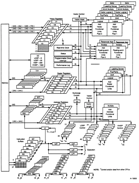
The CRAY Y-MP C90 mainframe contains the CPUs, an I/O section, an interprocessor communication section, a real-time clock, and central memory. Figure 1-2 is a block diagram of a CRAY Y-MP COO mainframe showing one CPU with the maximum I/O configuration. Each CPU has a computation section consisting of operating registers, functional units, and a control section.
The control section determines instruction issue and coordinates the three types of processing (vector, scalar, and address). The I/O section,
interprocessor communication section, real-time clock, and central memory are shared by the CPUs and are called shared resources.
( (AO) + (Ak) ) • ( (AO) + (Vk) )
( (AO) + (Ak) ) , ( (AO) + (Vk) )
( (AO) + (Ak» , ( (AO) + (Vk) )
TOO
( (Ah) + (nm) )
(AO)
( (Ah) + (nm) )
o
37
SI *Si
I/O
LDSP-6 LDSP-20 HISP-200 VHISP-1800
SI *SI
Vector Con1rol
Si
Exchange Control
Ai
Floating-point Functional
Units Pipe 0
Floating-point Functional
Units
Pipe 1
Add
Scalar Functional
Units
Ak
Ak
NOTE: *Con1rol and/or data from other CPUs.
[image:21.612.77.555.74.702.2]A-10505
Cpmputer System Overview
I/O Subsystem
CRAYY-MP C90 System Programmer Reference Manual
All CRAY Y-MP
coo
computer systems include an IOS-E; a second 10S-E is optional. The IOS-E is designed for rapid data transfer between the 10S-E's buffer memory and front-end computers, peripheral devices, and storage devices. The IOS-E also transfers data between its buffer memory and the mainframe's central memory.Each IOS-E contains up to eight I/O clusters depending on the site specifications. An I/O cluster comprises four I/O processors (EIOPs), each with four independent I/O buffers and four channel adapters. Each channel adapter is dedicated to a specific peripheral device. Each I/O cluster also includes a dedicated low-speed (LOSP) channel and two dedicated high-speed (HlSP) channels.
Each EIOP controls different portions of the system. Each EIOP has a memory section, a control section, a computation section, and an I/O section. I/O sections are independent and control some portion of the total I/O data stream for the lOS-E. 10S-E hardware allows
simultaneous data transfers between the EIOPs and the mainframe's central memory over HISP channels.
The 10S-E also provides connections to the High Performance Parallel Interface (HIPPI) channel. The HIPPI channel connects external peripheral equipment, such as high-speed graphic devices, to the mainframe. CRI does not provide external peripheral equipment but does provide the hardware connections and software drivers for the HIPPI channel.
Figure 1-3 shows the minimum configuration for a CRAY Y-MP C90 computer system with two I/O clusters. For more information on the 10S-E, refer to the lOS Model E System Programmer Reference Manual, publication number CSM-1010-000.
SSD-E Solid-state Storage Device
1-4
The SSD-E is an optional high-performance device used for temporary data storage. The SSD-E transfers data between the mainframe's central memory and the SSD-E through special very high-speed (VHISP) channels. The actual speed of these transfers depends on the SSD-E and CRAY Y-MP C90 system configuration. The SSD-E can also be
connected directly to an lOP through a HISP channel pair.
For more information on the SSD-E, refer to the SSD Solid-state Storage
Device System Programmer Reference Manual, publication number
CSM-1116-000.
o o I o o o
-II Ports
I I I I
I CPU
I 0
I
I ~
I I I I
N
f \
010OlCD
CRAY Y-MP C90 Ports Qa
~
'--./.
~~ "'3:3: CD
~3
0 0
a-<
---
CPU ~\ 1
\ \ \ \ \ ~ \ \ \
·
\ \·
\ \·
KEY"-LOSP - Low-speed channel (6 Mbytes,ls) HISP - High-speed channel (200 Mbytes,ls) VHISP - Very high-speed channel (1.800 Mbytes,ls)
G1il--~
I
JcB
Control Subsystem NetY.QrkIOPMUX
~ OWS
CCA-1
EIOP CCA-1
•
CRIFEI-1 (Front-end Computer)0 CCA-1 NSC N130 I (Front-end Computer) CCA-1
OCA-2 I
-EIOP DCA-2 I - - - 1 Each t - - 1 Each
:I: 00-60 00-60
en (§ 1 DCA-2 I - - - 16GB I - - 16GB
""0 OCA-2
OJ
0 ~ DCA-2 I
-0 EIOP 1 Each 1 Each
:::l CD DCA-2 I
-00-60 t - - 00-60 q (i1
Q. 2 OCA-2 I - - - 16GB t - - 16GB OCA-2 1 0 - ~
OCA-2 t
-EIOP DCA-2 I - - - 1 Each 00-60 10- 1 Each
3 DCA-2 I - - - 16GB Io- 00-60 16GB DCA-2 1 0
-
---
SSO-EI
Maintenance Channel(To MWS)
(Optional)
J
•
DCA-2 I-EIOP DCA-2 I - - - 8 Each I - - 8 Each
0 DCA-2 I - - - 00-60 16GB I - - 00-60 16GB
OCA-2 ~
DCA-2 t
-EIOP DCA-2 I - - - 8 Each 8 Each
00-61 I - - 00-61
:I:
(§ 1 DCA-2 I - - - 17GB I - - 17GB
en DCA-2 ~
""0 OJ
0
~ TCA-1 I
-0 EIOP TCA-1 I - - - IBM t - - IBM
~ CD
(i1 Controller Controller Q. 2 TCA-1 f - - t
-TCA-1 ~
HCA-3 r---t Input I
EIOP HCA-4 f---I Output I UltraNet
3 HCA-3 HCA-4
•
IOPMUX1 Each 00-60
t - - 16GB
~ ~
1 Each 00-60
t - - 16GB
~ ~
1 Each 00-60
t - - 16GB
-8 Each 00-60
t - - 16GB
~ ~
8 Each 00-61
I - - 17GB
~
IBM
~ Controller
-•
Input IOutput I
1 Each 00-60 16GB 1 Each 00-60 16GB 1 Each 00-60 16GB 8 Each 00-60 16GB SEach 00-61 17GB IBM Controller HIPPI
NSC EN641 J (Local Area Network) ... ~ ...
}
}
High-perf ormance Disks Economical Disk FannMagnetlcli apes 400ACS andiorSTK4
High Perfonnance Parallel ytes,ls Interface - 800 Mb
A-9696
Figure 1-3. Minimum CRA Y Y -MP C90 Configuration with Two I/O Clusters
-<
~ ""0o
<0 o en '< enr+ <D 3 ""0
a
(Q -, w 3 3 ~ :D~
-, <D ::J o CD ~ W ::J C Q!. o o 3 "'C C r+ <D -, (J)'< en
r+ <D 3 o < <D
<
<DOComputer System Overview
Disk Storage Units
Network Interfaces
CRAYY-MP C90 System Programmer Reference Manual
The CRAY Y-MP C90 computer system uses CRI disk storage units (DSUs) for mass data storage. A disk controller unit (DCU) serves as the interface between the DSUs and an EIOP. The EIOP and the DCU can transfer data between the EIOP and multiple DSUs without missing data or skipping revolutions. For more information on the DSUs, refer to the
60 Series Disk Systems Guide, CRI publication number COM-1124-000.
The CRAY Y-MP C90 mainframe is designed to communicate easily with front-end computer systems and computer networks.
Standard front-end interfaces (PEls) connect either the I/O channels of the CRAY Y-MP COO mainframe or the 10S-E to front-end computer channels. These connections provide input data to the system and receive output from the system for distribution to peripheral equipment. An PEl compensates for differences in channel widths, machine word size, electrical logic levels, and control signals.
Some PEls are housed in a stand-alone cabinet located near the host computer, and others are installed directly into the front-end computer system. Operation of the PEl is transparent to both the front-end computer and CRI system users.
As an option, a fiber-optic link (F0L-3) is available for some PEls to provide front-end connections of up to 6,560 ft (2,000 m) and complete electrical separation from the CRAY Y-MP C90 computer system. The CRAY Y-MP C90 mainframe can be connected to computer networks directly or through a front-end computer system.
Operator and Maintenance Workstations
1-6
The operator workstation (OWS-E) and the maintenance workstation (MWS-E) are based on a Sun 4/370 SPARCstation, 12-s10t chassis. The SPARCstation is a Sun version of the reduced instruction set computer (RISC) architecture. A VMEbus is provided in slots 4 through 12 of the workstations.
Both workstations run the SunOS 4.1.1 operating system and
Open Windows 2.0 software; the MWS-E also runs the ME maintenance diagnostic software release, and the OWS-E runs the OWS-E software release. The Sun operating system is an enhanced version of UNIX; it combines features of UNIX System Laboratories, Inc.'s System V UNIX and Berkeley Software Distribution's version 4.3 UNIX.
The OWS-E is part of the CRAY Y -MP C90 computer system. The MWS-E is owned by CRI and is supplied as part of the maintenance contract; it enables CRI engineers to perform system maintenance independent of any customer activity on the system.
The OWS-E and MWS-E communicate through the Control Subsystem Network, which is a dedicated, modified, Ethernet cable link used only for maintenance and control-related functions.
The OWS-E provides a dedicated workstation that Cray Research
analysts and customer operators use to operate, administrate, and monitor a Cray Research computer system. The OWS-E is also used for system boot, dump, and clear operations and for software and upgrade support.
The OWS-E communicates with the CRAY Y-MP C90 computer system through a LOSP channel from EIOP 0 in the lOS-E. The LOSP channel allows the mainframe to use the tape drives, disk drives, printer, and time-of-day clock. The OWS-E also provides an Ethernet interface to network workstations in a multiple-system site or for multiple-system operators.
The MWS-E provides multiple connections for hardware maintenance and monitoring of t1::: CRAY Y-MP C90 computer system. The MWS-E supports CRI diagnostics, enhanced diagnostic displays, code simulation, and maintenance and error channels. It monitors environmental
conditions and can shut down the system if severe variances occur. The MWS-E also serves as a platform for remote support, with customer approval. The MWS-E communicates with the CRAY Y-MP C90 computer system through a LOSP maintenance channel from the I~S-E.
Refer to the following publications for additional information on the OWS-E and MWS-E:
•
•
•
MWS-E User Guide, CRI publication number CDM-1123-0AO.
Operator Workstation (OWS) Guide, CRI publication number SN-3030.
2
CPu SHARED RESOURCES
Central Memory
Memory Instructions
CSM-0500-000
All central processing units (CPUs) in the CRAY Y-MP C90 mainframe share the following resources:
• Central memory • I/O section
• Interprocessor communication section • Real-time clock
Central memory consists of solid-state, random-access memory (RAM) that is shared by all the CPUs and the I/O section. Each memory word consists of 80 bits: 64 data bits and 16 error-correction bits (check bits). Storage for data and check bits is provided by 256 Kbyte
x
4 bit bipolar complementary metal oxide semiconductor (BiCMOS) chips with a 15-ns access time. In order to improve memory access speed, central memory is divided into multiple banks that can be active simultaneously. The banks have a 6-clock period (CP) cycle time; each bank can be accessed once every 6 CPs.In each CPU, the operating registers, instruction buffers, and exchange package have access to central memory through memory ports. Each CPU has four ports. Each of these ports is 2 words wide, allowing up to eight simultaneous memory references from each CPU. The I/O section shares one port in each CPU.
Table 2-1 shows all the CPU machine instructions that transfer data between CPU registers and central memory, or that affect memory operation. The contents of the data base address (DBA) register are added to instruction-generated memory addresses to form absolute memory addresses. Refer to "Absolute Memory Address Calculating" later in this section.
Table 2-1. Memory Instructions
Machine CAL Type of
Instruction Syntax Description Memory Reference
10hiOO nm Ai exp,Ah Read from ((Ah) + exp + (DBA» to Ai. Scalar 11hiOO nm exp,Ah Ai Write (AI) to ((Ah) + exp + (DBA).
12hiOO nm Si exp,Ah Read from ((Ah) + exp + (DBA» to Si. 13hiOO nm exp,AA Si Write (Sz) to ((All) + exp + (DBA).
034ijk Bjk,Ai ,AO Read (AI) words starting at address (AO) + Block Transfer (DBA) to B registers starting at register jk.
035ijk ,AO Bjk,Ai Write (AI) words from B registers starting at register jk to memory starting at (AO) + (DBA). 036ijk Tjk,Ai ,AO Read (AI) words starting at address (AO) +
(DBA) to T registers starting at register jk. 037ijk ,AO Tjk,Ai Write (AI) words from T registers starting at
register jk to memory starting at (AO) + (DBA).
176iOk Vi ,AO,Ak Read (VL) words to Vi starting at address Stride (AO) + (DBA), incrementing by (Ak).
1770jk ,AO,Ak Vj Write (VL) words from (VJ) to memory starting at address (AO) + (DBA), incrementing by (Ak).
176i1k Vi ,AO,Vk Read (VL) words to Vi using memory Gather addresses ((AO) + (Vk) + (DBA».
1771jk ,AO,Vk Vj Write (VL) words from (VJ) to memory using Scatter memory addresses ((AO) + (Vk) + (DBA».
002300 ERI Enable interrupt on operand range error. None
002301 EBP Enable interrupt on breakpoint.
002400 DRI Disable interrupt on operand range error.
002401 DBP Disable interrupt on breakpoint.
002500 DBM Disable bidirectional memory transfers.
002600 EBM Enable bidirectional memory transfers.
002700 CMR Complete memory references.
CRAY Y-MP C90 System Programmer Reference Manual CPU Shared Resources
Machine CAL
Instruction Syntax
002705 CPR
002706 CPW
CSM-0500-000
Table 2-1. Memory Instructions (continued)
Type of
Description Memory Reference
Complete port reads. None
Complete port writes.
Instructions 10h through 13h perform scalar references; each instruction causes only 1 word to be transferred to or from memory. Instructions
034ijk through 037ijk perform block transfers. Each instruction transfers
a block of from 1 to 127 words to or from consecutive locations in memory. Instructions 176iOk and 1770jk perform stride references. A block of from 1 to 128 words are transferred to or from memory
locations separated by a constant increment (stride). Instructions 176ilk and 1771jk perform gather and scatter references. These instructions transfer from 1 to 128 words to or from randomly programmable locations in memory.
Instructions 002300 through 002706 affect memory operation.
Instructions 002300 and 002400 set and clear the interrupt-on-operand range error (lOR) interrupt mode. When this interrupt mode is set and". enabled, it allows interrupts on operand range errors. Refer to "Address Range Checking" in this section for a more complete explanation. Instructions 002301 and 002401 set and clear the interrupt-on-breakpoint (IBP) interrupt mode. When this interrupt mode is set and enabled, it
allows interrupts on write references within the breakpoint range, which should be set previously by instruction 0017jk.
Instructions 002500 and 002600 disable and enable the bidirectional memory mode. When this mode is enabled, block read and write operations can operate concurrently. When this mode is disabled, only block read operations can operate concurrently.
Instruction 002700 ensures completion of all memory references within the particular CPU issuing the instruction. Instruction 002700 does not issue until all previous memory references can complete in a fixed number of CPs. For example, a CPU is assured of receiving updated data when it issues a memory read instruction after instruction 002700. Used in conjunction with semaphore instructions, this instruction synchronizes memory references between processors.
Instructions 002704 through 002706 can be used to ensure sequential memory referencing within a CPU. These instructions do not issue until all previous memory references are at a stage of execution such that they
Logical Organization
Memory Paths
can run to completion before any subsequent memory references. Instruction 002704 ensures that all read and write references are at this stage. Instruction 002705 ensures that all read references are at this stage, and instruction 002706 ensures that all write references are at this stage.
In addition to direct memory references generated by CPU machine instructions, there are three ways that memory references are generated indirectly. First, a no-coincidence condition in a CPU causes an
instruction fetch sequence to begin, during which 32 consecutive words are read from central memory to an instruction buffer. Second, an exchange sequence in a CPU causes 16 words to be read from and 16 words to be written into central memory. (For details on the fetch and exchange sequences, refer to "Exchange Mechanism" and "Instruction Fetch Sequence" in Section 3 of this manual.) The third type of indirect memory reference occurs when an I/O transfer to or from an external device causes a block of words to be read from or written to central memory. For details on I/O transfers, refer to "I/O Section" in this section.
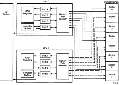
Figure 2-1 shows a CPU's memory ports and paths to central memory. Refer to this figure while reading the following paragraphs. Central memory is divided into 8 sections. Each section is divided into 8 subsections, and each subsection contains two 8-bank groups. This makes a total of 1,024 banks. This arrangement permits simultaneous memory references (two or more memory references that begin in the same CP) and overlapping memory references (one or more memory references that begin while another reference is in progress).
Each CPU has an independent path into each memory section. (The I/O section does not have its own paths, but shares the paths of each CPU.) Independent paths allow each CPU to make up to eight simultaneous memory references, one reference to each section. Each CPU can have overlapping references in different sections without restrictions or within a section as long as each reference uses a different subsection.
CRAY Y-MP C90 System Programmer Reference Manual CPU Shared Resources
1/0
Section
Memory Ports
CSM-0500-000
CPU 0 Central Memory
Section
H
PortAr--
r---'"
0CPU Registers
H
PortSr--
MemoryI
I
Path
I
r - - - ' " Section
Selection 1
H
PortC ~Ii
~
-Instruction
if=l
Port 0I--
~-llr--"
SectionSuffers 2
Iii
Section
Ill r - -..
III 3
III
I
I " I Section
I l l l r - "
CPU n III 4
I "
'I
+-t
PortA ~ IIIII SectionCPU
-
.. _____ ...J
!!
IIr'"
5Registers _ _ --1 I I I !
~ PortS
J.-
Memory Path--
_____ .J
IIISelection
______ .J
IISection
-H
Port C1---
...
...
r- -________ ...J
!
r'"
6~---~I
Instruction
if=l
Port 0I--
...
!---I
SectionSuffers
...
---
..
7
[image:30.613.90.549.76.403.2]A-9640
Figure 2-1. Central Memory Architecture
Simultaneous and overlapping memory references involving two or more CPU s have fewer restrictions than those involving a single CPU.
Simultaneous and overlapping memory references from different CPU s can occur within a section and a subsection; however, each reference must use a different bank.
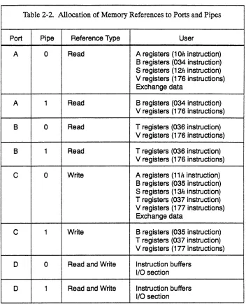
Each CPU has four memory ports through which the CPU accesses its paths to central memory. Each port contains two pipes, allowing up to eight simultaneous memory references per CPU. Table 2-2 lists the specific read and write references allocated to each of the ports and pipes.
Table 2-2. Allocation of Memory References to Ports and Pipes
Port Pipe Reference Type User
A 0 Read A registers (10h instruction)
B registers (034 instruction) S registers (12h instruction) V registers (176 instructions) Exchange data
A 1 Read B registers (034 instruction)
V registers (176 instructions)
B 0 Read T registers (036 instruction)
V registers (176 instructions)
B 1 Read T registers (036 instruction)
V registers (176 instructions)
C 0 Write A registers (11 h instruction)
B registers (035 instruction) S registers (13h instruction) T registers (037 instruction) V registers (177 instructions) Exchange data
C 1 Write B registers (035 instruction)
T registers (037 instruction) V registers (177 instructions)
D 0 Read and Write I nstruction buffers
I/O section
D 1 Read and Write Instruction buffers
I/O section
Ports A, B, and C are used by memory reference instructions and by the exchange sequence. Port D is used by the instruction buffers and the I/O section. With the exception of memory reads to vector (V) registers (instructions 176iOk and 176i1k), each type of memory reference uses one specific port. On a read to a V register, port B is used if available. If
port B is reserved, port A is used if available. If both ports are reserved, the instruction holds issue until one of the ports is available. If both ports become available at the same time, port B is used.
CRAY Y-MP C90 System Programmer Reference Manual CPU Shared Resources
Ports A, 8, and C
CSM-0500-000
and T register block transfers, the first word transferred always uses pipe 0, and the next word uses pipe 1; subsequent words alternate between the two pipes until the transfer is complete.
Ports A, B, and C operate differently for block and vector transfers than for scalar transfers. A memory reference instruction that transfers data to or from B, T, or V registers holds issue if the associated port is in use by another memory operation. When the port becomes available, the instruction issues and reserves the port. The port remains reserved until the instruction completes all its memory references. The port reservation is then cleared, making the port available for other memory operations. A block or vector transfer normally reads or writes 2 words of data each clock period (CP). However, if the instruction encounters a memory conflict during its execution, it temporarily suspends operation until the conflict is resolved. Therefore, the number of CPs the instruction runs and the number of CPs the port is reserved are unpredictable. Refer to "Conflict Resolution" in this section for additional information on port conflicts.
Block and vector transfer instructions that use different ports normally operate simultaneously. Under some circumstances, this mode of operation can cause memory references to occur in an unwanted sequence. For example, if instruction 035ijk (write to memory from a
block ofB registers) precedes instruction 176iOk (read from memory to a
V register) and both instructions reference one or more of the same memory addresses, data from some memory addresses may be read before the new data is written to them. Both of these instructions can operate simultaneously, and the read instruction may reference an address before the write instruction.
There are several ways to prevent out-of-sequence references.
Instruction 002700 (complete memory references), instruction 002704 (complete port reads and writes), or instruction 002706 (complete port writes) can be inserted between the write and read instructions. Although these instructions do not perform any operation, they prevent the read instruction from issuing until the write instruction completes all its memory references and clears the port C reservation. Usually,
instructions 002704 and 002706 are used to insure sequential memory referencing within a CPU, and instruction 002700 is used to synchronize memory references between CPUs.
Clearing the bidirectional memory (BDM) mode in the exchange package also prevents out-of-sequence memory references. In this case, instructions that use port A or B also require port C to be available, and instructions that use port C require ports A and B to be available. The memory read instruction holds issue until the write instruction completes all its memory references.
Port D
Conflict Resolution
Section Conflict
Before it can issue, a scalar transfer instruction requires that ports A, B, and C be available to ensure sequential operation between block transfers and scalar references within a CPU. A scalar reference conflict is
detected in CP 4 of execution. If a conflict occurs, up to two additional scalar references are still allowed to issue. A fourth scalar reference holds issue if the first reference still has a conflict. Scalar references always execute in the order they are issued within a CPU.
An instruction fetch sequence has priority over an I/O transfer in port D. That is, if a fetch request occurs while an I/O transfer is in progress, the I/O transfer is suspended and the fetch begins. When the fetch
completes, the I/O transfer continues.
A memory conflict occurs whenever a memory port tries to access a shared part of memory in use, or whenever two or more ports try to access a shared part of memory at the same time. Intra-CPU conflicts involve ports in the same CPU. Inter-CPU conflicts involve ports in different CPUs. In both cases, conflict resolution logic uses predefined priority schemes to sequence the conflicting memory references and to maximize overall machine throughput.
There are five types of memory conflicts: section, subsection,
simultaneous subsection access, bank busy, and write bank busy. The following paragraphs explain each type of conflict and how the conflict is resolved.
A section conflict occurs when two or more ports in the same CPU simultaneously attempt to access the same memory section. A section conflict occurs because there is only one path from each CPU to each memory section. The port with the highest priority level and no
subsection conflict is allowed to begin its reference. All other conflicting ports hold reference for 1 CPo The following rules determine priorities between conflicting ports:
CRAY Y-MP C90 System Programmer Reference Manual CPU Shared Resources
Subsection Conflict
CSM-0500-000
•
•
•
Port D normally has a lower priority than ports A, B, and C when it
is used for an I/O transfer. However, if a port D I/O memory reference is forced to hold for 32 CPs, port D is temporarily given top priority so that one memory reference can proceed. Port D returns to a low-priority status after the reference begins.
Among ports A, B, and C, any port that has an odd memory address increment has priority over ports that have an even increment. The following rules determine the type of increment (even or odd) for each port:
•
•
•
A port used by a block reference instruction has an address increment of 1, which is odd.
A port used by a stride reference instruction can have any constant increment (even or odd).
A port used by a gather or scatter instruction can have an increment that changes after each reference. For the purpose of conflict resolution, a gather or scatter instruction is always considered to have an odd increment.
Among ports A, B, and C with the same type of memory
increment, priority is determined by the relative time of instruction issue. The port used by the instruction first issued has the highest priority.
Subsection conflicts occur because each memory reference by a CPU makes an entire memory subsection unavailable to all ports in the same CPU for 7 CPs. A subsection conflict occurs if any port in the same CPU attempts to make a reference to the same subsection during this interval. The new reference holds for 1 to 6 CPs until the old reference no longer needs the subsection. Subsection conflicts usually involve two or more ports, but may involve two references from the same port.
If two or more references are holding issue because of the same
subsection conflict, a section conflict occurs immediately following the resolution of the subsection conflict. Another subsection conflict occurs 1 CP after the section conflict. For example, if port A is using a
subsection and ports Band C attempt to use the same subsection while it is busy, ports Band C hold issue because of the subsection conflict. When the reference from port A no longer needs the subsection, the subsection conflicts disappear. Ports B and C are involved in a section conflict, which is resolved according to the priority rules previously described. The port with the higher priority makes its reference, and the port with the lower priority encounters a subsection conflict.
Simultaneous Subsection Access Conflict
Priority Count
0
1
2
3
4
5
6
7
10
11
12
13
14
15
16
17
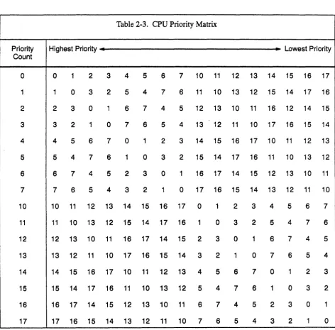
Simultaneous subsection access conflicts occur when two or more ports in different CPUs attempt to access the same memory bank group at the same time. The CPU with the highest priority is allowed to make its reference. All other CPUs attempting to access the same bank group hold their references for 1 CPo Relative priorities between CPUs are determined by the value stored in a priority counter. This value
[image:35.615.77.550.259.725.2]increments by 1 each CPo For a given value of the priority counter, each of the CPUs is assigned the priority shown in Table 2-3. For example, if the priority count is 5, then CPU 5 has the highest priority and CPU 12 has the lowest priority. Following a simultaneous subsection access conflict, each CPU port forced to hold a reference encounters a bank-busy conflict.
Table 2-3. CPU Priority Matrix
Highest Priority 4 • Lowest Priority
0 1 2 3 4 5 6 7 10 11 12 13 14 15 16 17
1 0 3 2 5 4 7 6 11 10 13 12 15 14 17 16
2 3 0 1 6 7 4 5 12 13 10 11 16 12 14 15
3 2 1 0 7 6 5 4 13 12 11 10 17 16 15 14
4 5 6 7 0 1 2 3 14 15 16 17 10 11 12 13
5 4 7 6 1 0 3 2 15 14 17 16 11 10 13 12
6 7 4 5 2 3 0 1 16 17 14 15 12 13 10 11
7 6 5 4 3 2 1 0 17 16 15 14 13 12 11 10
10 11 12 13 14 15 16 17 0 1 2 3 4 5 6 7
11 10 13 12 15 14 17 16 1 0 3 2 5 4 7 6
12 13 10 11 16 17 14 15 2 3 0 1 6 7 4 5
13 12 11 10 17 16 15 14 3 2 1 0 7 6 5 4
14 15 16 17 10 11 12 13 4 5 6 7 0 1 2 3
15 14 17 16 11 10 13 12 5 4 7 6 1 0 3 2
16 17 14 15 12 13 10 11 6 7 4 5 2 3 0 1
CRAYY-MP C90 System Programmer Reference Manual CPU Shared Resources
Bank-busy Conflict
Write Bank-busy Conflict
Conflict Type
Section
Intra-CPU
Subsection
Intra-CPU
Simultaneous
Inter-Subsection CPU
Access
Bank-busy
Inter-CPU
Write
Inter-Bank-busy CPU
CSM-0500-000
Bank-busy conflicts occur because each memory reference by a CPU makes the referenced memory bank unavailable to all ports in all other CPUs for 6 CPs. A bank-busy conflict occurs if any port in a different CPU attempts to make a reference to the same bank during this interval. The new reference holds from 1 to 5 CPs until the old reference no longer needs the bank. If two or more CPUs are holding because of the same bank-busy conflict, a simultaneous subsection access conflict occurs immediately following resolution of the bank-busy conflict.
Write bank-busy conflicts occur because within a subsection each write data path is shared between two memory banks. Banks 0 and 4, 1 and 5, 2 and 6, and 3 and 7 share write data paths. When a write reference is made by a CPU to a memory bank, both memory banks in the pair are unavailable to all ports in all other CPUs for 6 CPs. A write bank-busy conflict occurs if any port in a different CPU attempts to make a reference to either bank during this interval. The new reference holds from 1 to 5 CPs until the old write reference no longer needs the bank. ·'If two or more CPUs are holding because of the same write bank-busy conflict, a simultaneous subsection access conflict occurs immediately following resolution of the write bank-busy conflict. Table 2-4 summarizes the five types of memory conflicts.
Table 2-4. Memory Conflicts
Duration Resolution Comment
1 CP The highest-priority port with Followed by a subsection no subsection conflict makes conflict if references are made reference. Other ports hold to the same subsection. reference.
1 to 6 Memory references for the Followed by a section conflict CPs port hold until the reference in if two or more references are
progress is complete. forced to hold.
1CP The highest-priority CPU Followed by a bank-busy makes reference. Other conflict in each CPU that was
CPUs hold reference. forced to hold.
1 to 5 Memory references for the Followed by a simultaneous CPs port hold until the reference in subsection access conflict if progress is complete. two or more references are
forced to hold.
1 to 5 Memory references for the Followed by a simultaneous CPs port hold until the write subsection access conflict if reference in progress is two or more references are
complete. forced to hold.
Memory Addressing
Memory addresses are 29 bits long, allowing up to 512 Mwords of storage to be referenced. Figure 2-2 shows the function of each address bit. In each of the section, subsection, and bank-select fields, the highest-numbered bit is most significant. With this arrangement, if the memory address advances sequentially, all memory sections are stepped through in tum. Next, all subsections are stepped through, then each bank group, and finally all banks are stepped through.
Bank Group
228 227 226 225 224 223 222 ~1 220 219 2 18 217 216 2 15 214 213 212 211 210 209 208 207 206 205 204 203 202 201 200
Internal Chip Address
1
Internal Chip Address Bank1
Subsection SectionSelect Select Select
Chip Select
Figure 2-2. Memory Addressing
Group
Select A·9637
Address bits 26 through 23 collectively make up the bank group number. Thus, subsection 5 (1012) in group 1 has a bank group number of 15. The bank group numbers run from 00 through 178.
The chip select bit is used to select one of two physical groups of chips on the memory module. The internal chip address selects a group of four bits on a 256 Kbyte X 4 bit memory chip.
Absolute Memory Address Calculating
Memory reference instructions listed in Table 2-1 calculate absolute memory addresses by adding combinations of the following values.
•
•
•
•
A register contents V register contents DBA register contents
Three-parcel instruction nm field contents
CRAY Y-MP C90 System Programmer Reference Manual CPU Shared Resources
Address Range Checking
DBA Register
DLA Register
CSM-0500-000
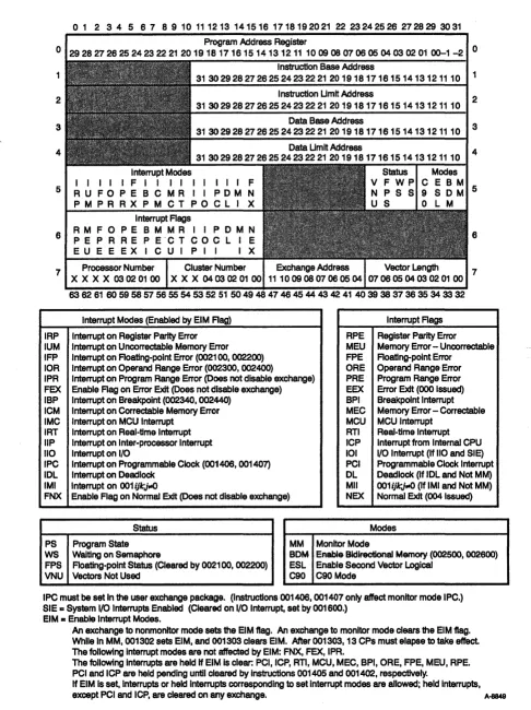
Four registers in the exchange package place program data and instruction areas in specific locations in memory and allocate specific amounts of memory to the areas. These registers allow all programs to be relocated. When a program is written, the programmer does not need to know where the instruction and data areas are located in memory. These registers also enable the programmer to restrict certain parts of memory from any program. A program can be halted if it tries to perform an instruction outside of its allowed instruction area or if it tries to read or write data outside of its allowed data area. When more than one program occupies memory at the same time, programs can be prevented from performing instructions or operating on data that belongs to other programs.
The data base address (DBA) register determines where the data area of a program begins in memory. Data addresses generated by memory reference instructions are relative to the DBA. The absolute address of any memory location is determined by adding the DBA to the address~.
generated by the memory reference instruction. Refer again to Table 2-1 for a list of memory reference instructions.
The data limit address (DLA) register determines the highest absolute memory address the program can use for reading or writing data. Each time an instruction makes a memory reference, the absolute memory address generated is compared to the values stored in the DBA and DLA registers. If the absolute memory address is between the DBA and DLA, the reference is allowed to proceed. Otherwise, an out-of-range
condition exists and the memory reference is aborted by disabling all chip selects and write enables in the referenced memory bank. For a memory write reference, no write operation is performed. For a memory read reference, all bits are set to O.
If the interrupt-on-operand range (lOR) interrupt mode is set in the exchange package, an out-of-range condition sets the operand range error (ORE) interrupt flag and causes an exchange sequence to begin. If the lOR interrupt mode is not set, the program continues to run.
IBA Register
ILA Register
The instruction base address (IBA) register functions similarly to the DBA register, except that it operates on the instruction area of a program. Each time an instruction fetch sequence takes place, absolute memory addresses are formed by adding the relative addresses generated by the fetch control logic to the contents of the IBA register.
The instruction limit address (ILA) register functions similarly to the DLA register, except that it operates on the instruction area of a program and does not provide for continuing program execution when an
out-of-range condition occurs. If an absolute memory address generated by an instruction fetch sequence is between the IBA and ILA, the fetch sequence is allowed to proceed. Otherwise, an out-of-range condition exists. An out-of-range condition sets the program range error (PRE) interrupt flag in the exchange package and causes an exchange sequence to begin.
The DBA, DLA, IBA, and ILA registers contain only address bits 210 and above. Bits 2° through 29 are always 0; therefore, the content of these registers is always a multiple of 20008 (1,02410). Adding the contents of the DBA or IBA register to a relative memory address does not change the section, subsection, or bank number. Therefore, memory conflicts can be determined from the relative addresses generated by instructions and the fetch control logic. It is not necessary to use absolute memory addresses to determine whether conflicts exist.
Address range checking is not performed during exchange sequences and I/O transfers. Memory addresses generated by these operations are absolute memory addresses.
Error Detection and Correction
Single-byte correctiOn/double-byte detection (SBCDBD) monitors central memory for data errors. Memory errors involving only one 4-bit byte in each data word ( single-byte errors) can be detected and corrected by the hardware. Double-byte errors can be detected but cannot be corrected. Errors involving more than 2 bytes cannot be reliably detected.
CRAY Y-MP C90 System Programmer Reference Manual CPU Shared Resources
CSM-0500-000
OR (XOR) operation. The resulting comparison is called a syndrome code. If all the bits in the syndrome code are 0, the 2 checkbytes are identical and no memory error occurred.
If there are one or more 1 bits in the syndrome code, some type of memory error occurred. The type of memory error (single-byte or double-byte) can be determined by interpreting the syndrome code. If a single-byte error occurs, the syndrome indicates the bit or bits within that byte that are in error. The SBCDBD logic toggles the incorrect bit or bits to the correct value. If a double-byte error occurs, the syndrome code indicates that there is an error, but it cannot pinpoint the incorrect bits. Errors involving more than 2 bytes produce unpredictable results. In some cases, errors produce unique syndrome codes that can be detected by the SBCDBD logic. In other cases, the syndrome code appears to be a no-error condition or a single- or double-byte error.
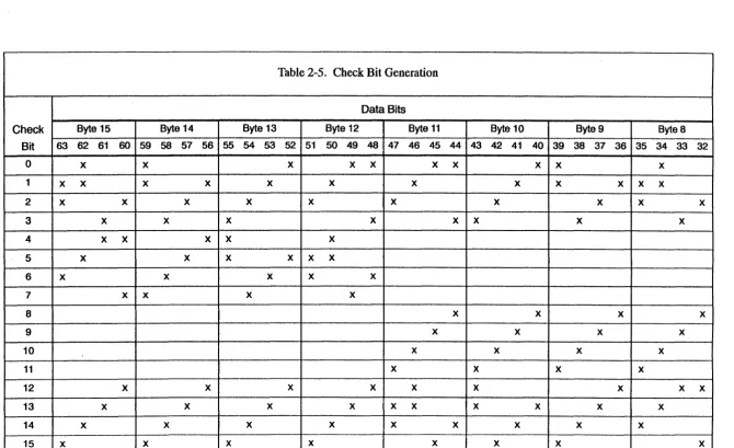
Table 2-5 shows the data bits used to generate each bit in the checkbyte. All data bits marked with an X in a row contribute to the corresponding check bit. The parity of all data bits marked with an X determines the state of the check bit. If the parity is even, the check bit is set to O. If it is odd, the check bit is set to 1. For example, the data bits used to
generate check bit 3 are bits 23, 27,211,215,233,238,243, 244, 248, 255, 208, and 261. If an even number of these bits is 1, check bit 3 is set to logic
b;
otherwise, it is set to logic 1.If a syndrome code other than all O's is generated, memory error information is sent to the error ch.annel to help pinpoint the hardware failure. A nonzero syndrome code may also initiate an exchange sequence, depending on the state of two of the interrupt modes in the exchange package. If the interrupt-on-correctable memory error (ICM) interrupt mode is set, a single-byte (correctable) memory error sets the memory error - correctable (ME C) interrupt flag in the exchange package and starts an exchange sequence. If the
interrupt-on-uncorrectable memory error (IUM) interrupt mode is set, a double-byte or detectable multiplebyte (uncorrectable) error sets the memory error -uncorrectable (MEU) interrupt flag and starts an exchange sequence. If either the ICM or the IUM interrupt mode is not set, the corresponding memory error does not start an exchange sequence and does not set an interrupt flag.
(')
en
3: • o 01 o o I o o oCheck Bit 63
0
1
x
2
x
3 4 5
6
x
7 8 9 10 11 12 13 14 15 x
Byte 15 Byte 14 62 61 60 59 58 57
X X
x
x
x
x
x
x
x x
x
x
x
X XX
x
x
X
x
[image:41.794.76.746.88.497.2]X
Table 2-5. Check Bit Generation
Data Bits
Byte 13 Byte 12 Byte 11
56 55 54 53 52 51 50 49 48 47 46 45
X X X X
x
x
x
x
x
x
x
x
x
x x
x
x
x x x
x
x
XX
x
x
x
x
X
x
x
x
x
x
x x
X
x
x
x x
x
Byte 10 Byte 9
44 43 42 41 40 39 38 37
X X X
x
x
x
x
x x
x
x
x
x
x
x
x
x
x
x
x
x
x
x
x
x
x
x
Byte 8 36 35 34 33