Available Online at www.ijpret.com 310
INTERNATIONAL JOURNAL OF PURE AND
APPLIED RESEARCH IN ENGINEERING AND
TECHNOLOGY
A PATH FOR HORIZING YOUR INNOVATIVE WORK
REVIEW OF 32 BIT ARITHMETIC ADDER USING REVERSIBLE LOGIC
SHUBHASHREE M. DAMLE, S.G.MUNGALEDepartment of Electronics Engineering, Priyadarshini College of Engineering Nagpur, India
Accepted Date: 15/03/2016; Published Date: 01/05/2016
\
Abstract: For mathematical representation or calculation of very large or small numbers, relatively large size is essential. These large range value can be represented by using IEEE 754 standard. This paper proposed the design of floating point arithmetic adder using reversible logic. Low Power dissipation and smaller area are most important factors while designing adder for digital circuits. Adders used in digital circuits generates large amount of heat whenever there is a transition of bits, reversible logic has emerged as a promising technology in reducing power dissipation. It has application in various fields such as low power VLSI, Quantum computing and Nanotechnology. This paper presents the design of reversible adder using reversible gates.
Keywords- Digital circuits, Full adder, Barrel Shifter, Garbage output, Reversible Logic, Reversible Gate, VHDL, Xilinx 9.2i.
Corresponding Author: MS. SHUBHASHREE M. DAMLE Access Online On:
www.ijpret.com
How to Cite This Article:
Available Online at www.ijpret.com 311 INTRODUCTION
In VLSI systems increase in number of transistors makes the system complex which further increase the power dissipation of the system. Also any Boolean function can be implemented by using logic of reversible logic gates as it has already been proved. When an input is applied to the reversible gate, a logical operation is performed and also there is loss of some information which is dissipated as heat. So we can conclude that power dissipation is the main concern for both producers and consumers. A reversible logic gate gives a unique output for each input. It has k-inputs and k-outputs, hence denoted by k*k. In a reversible circuit the input pattern can be reconstructed from the output pattern. The number of input and output are equal. In reversible logic there are more than one aspect to focus on number of gates used. There are many parameters which determine the complexity and performance of reversible circuits, they are as follows:
(A)Garbage Output:
Unwanted output of a reversible gate is known as garbage output, i.e., the outputs which are needed to maintain the reversibility.
(B)Delay:
The maximum number of gates in a path from any input signal line to any output line is the delay of a circuit.
(C)Quantum cost:
Quantum cost gives the cost of the circuit in terms of the cost of a basic gate. It is calculated from the number of basic reversible logic gates (1*1 or 2*2) required to realize the circuit.
For floating point calculations, IEEE standard 754 has been designed. In the proposed system binary 32 bit format (single precision) is used. This floating point number is divided in sign bit, exponent and mantissa.
Fig.1 Floating point Number Representation
1. BASIC REVERSIBLE GATES
Available Online at www.ijpret.com 312 each reversible gate is called quantum cost.1x1 reversible gates has zero quantum cost and quantum cost of 2x2 reversible gates is one. Any reversible gate can be realized by using 1x1 not gates and 2x2 reversible gates, such as V and V+ (V is square root of NOT gate and V+ is its hermitian). The V and V+ quantum gates have the following property:
V x V = NOT V x V+ = V+ x V = I V+ x V+ = NOT.
Hence quantum cost of a reversible gate can be calculated by counting the number V, V+ and CNOT.
2.1 Not Gate-
This is the only reversible gate among the conventional logic gates. This is a 1x1 gate with quantum cost of zero.
2.2 Peres Gate-
2.3Feynman Gate-
2.4Fredkin Gate-
2.5 Toffoli Gate-
Available Online at www.ijpret.com 313
2. PROPOSED PERES FULL ADDER
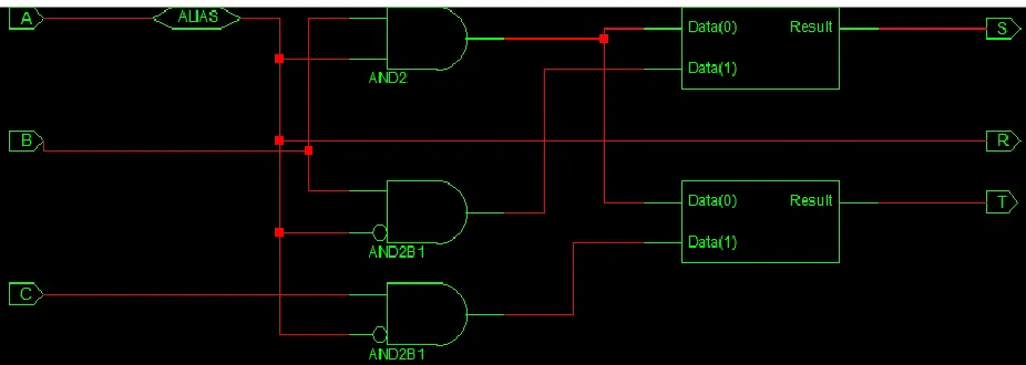
The peres gate is reversible 3*3 gate and quantum cost of peres gate is four having mapping input (P,Q,R) to output(X,Y,Z) is as shown in figure 1.
Fig.2 Peres Full Adder
4. REVERSIBLE ADDER
As shown in figure reversible floating point adder architecture, the 32 bit input is given to A& B. The 32 bit input is divided into sign bit, exponent and mantissa according to floating point standard IEEE 754. At first exponents are checked whether equal or not, if not smaller is incremented till it get matched with larger. For alignment of floating point
Fig.3 Proposed Reversible Adder Architecture
Available Online at www.ijpret.com 314 shift amount by which significant has been shifted. That necessary shift amount is provided to barrel shifter. The actual swapping will be done by using bank of fredkin gate which serve as a multiplexer. If exponent A< exponent B then only the number will swap positions otherwise it is passed to the next stage of architecture without swapping. The barrel shifter module can be designed by using combination of feynman gate and fredkin gate. It will perform six operations including right shift, left shift and rotate operation. The proposed conversion unit will work simultaneously as a sign magnitude to 2’s complement and 2’s complement to sign magnitude vice versa. By using combination of reversible half adder and single output fan-out feynman gate conversion is made. The value of conversion unit is forwarded to 28-bit ripple carry adder. This addition has been performed by combination of peres gate which work as a full adder. This sum is normalized and rounded to fit in 32- bit format. Conditional right shift, reversible leading zero counter and barrel shifter is used for normalization and rounding purpose.
5. RESULT
Fig. 4 and fig.5 shows the RTL schematic and simulation of Fredkin Gate.Fig.6 and fig.7 shows the RTL schematic and simulation of Feyman Gate.Fig.2 shows the block diagram of peres full adder. Proposed peres full adder is implemented and resulted by using VHDL and simulated in Xilinx 9.2 i. Fig.8 shows the RTL schematic diagram and fig.9 shows the simulated result.
Available Online at www.ijpret.com 315 Fig.5 Fredkin Gate Simulation
Fig.6 Feynman Gate Simulation
Available Online at www.ijpret.com 316 Fig.8 RTL Schematic of PERES Full Adder
Fig.9 Simulation Peres full Adder
6. CONCLUSION
Reversible gate are used to implement arithmetic circuit using full adder. This paper presents the design for 32 bit(single precision) reversible adder. The new reversible 4*4 peres gate full adder is proposed in this paper. Also the simulation of fredkin gate and feyman gate are shown which will be used for barrel shifter unit shown in fig.3. By using proposed peres full adder design of large reversible system is possible. Here the power consumption can be calculated and compare it with the irreversible adder. VHDL is used for implementing design of full adder and reversible gates and synthesis has been done using Xilinx 9.2i.
REFERNCES
Available Online at www.ijpret.com 317 2. IEEE standard for floating–point arithmetic. IEEE Standards Committee, Oct. 2006.
3. Martin S. Schmookler and Arnold Weinberger, “High Speed Decimal Addition IEEE
Transactions On Computers,” VOL. C-20, NO. 8, AUGUST 1971.
4. R. D. Kenney and M. J. Schulte, “High-speed multi operand decimal adders IEEE Trans. on Computers”, 54(8):953–963,Aug. 2005.
5. T. Nagababu, “A Low Power Adder Using Reversible Logic Gates” IJERT Volume 1 issue 3 Nov 2012.
6. Homework report, “Reversible Adder Implementation In VHDL”.
7. Mr Devendra goyal, “VHDL implementation of reversible logic gates”.
8. V. Kanalakannan, “Design Of Adder /Subtractor Circuits Based On Based On Reversible Logic Gate IJAREEIE”, vol 2 issue8 august 2013.”