www.adv-radio-sci.net/11/143/2013/ doi:10.5194/ars-11-143-2013
© Author(s) 2013. CC Attribution 3.0 License.
Radio Science
Design of RF MEMS based switch matrix for space applications
S. Di Nardo1, P. Farinelli2, T. Kim3, R. Marcelli4, B. Margesin5, E. Paola1, D. Pochesci6, L. Vietzorreck3, and F. Vitulli6 1ThalesAlenia Space, L’Aquila, Italy
2University of Perugia, Perugia, Italy
3Technische Universit¨at M¨unchen, Munich, Germany
4CNR – Institute for Microelectronics and Microsystems, Roma, Italy 5FONDAZIONE BRUNO KESSLER, Trento, Italy
6ThalesAlenia Space, Roma, Italy
Correspondence to: T. Kim ([email protected])
Abstract. RF MEMS based switch matrices have several ad-vantages compared to the mechanical or solid-state switch based ones for space applications. They are compact, light and less lossy with a high linearity up to high frequency. In this work, a 12×12 switch matrix with RF MEMS and LTCC technologies is presented based on the planar Benesˇ network. The simulated performance of the 12×12 switch matrix is below−12 dB IL (Insertion Loss) up to C band and −15 dB RL (Return Loss) up to Ku band. Moreover, it has a good isolation better than−50 dB. A 4×4 switch matrix with the same design process and technologies is fabricated and measured to verify the 12×12 switch matrix design pro-cess. The measured performance agrees very well to the sim-ulations.
1 Introduction
In a communication satellite, the received signals are simul-taneously to be delivered to the assigned transmission out-puts with high flexibility, which is normally achieved by high-order switch matrices. Microwave or millimeter-wave switch matrices provide a full and high connectivity to the satellite broadcasting system. The switch matrices which are used up to now are based on the mechanical switches. The mechanical switches are reliable, less lossy and can drive a high power with high linearity. However, they are slow, bulky, heavy and require motors for switching, which are normally unsuitable for the cost-effective high speed system. Switch matrices using solid state devices, such as PIN diodes, MESFETs (MEtal Semiconductor Field Effect Transistors) or HEMTs (High Electron Mobility Transistor), have been also discussed due to their high speed and compact size with
cheaper prices. However, they consume a DC power and may generate intermodulation spurious modes. Moreover, their applicable frequency bands are limited. Recently, Radio Fre-quency Micro Electro Mechanical System (RF-MEMS)s are referred to as a good candidate to get over the reported draw-backs of the mechanical or solid state based switches. They are small and virtually consume no power. RF MEMS can be operated up to high frequency with high linearity. Moreover, on maturing microfabrication technologies, the cost for RF MEMS fabrication is going down (De Angelis et al., 2012).
In the present paper, the design of the RF MEMS switch matrix is discussed. The aimed switch matrix has 12 inputs and 12 outputs. Starting from the network topology and the control algorithm, the design process for the 12×12 switch matrix is described including physical assembly with the control boards and the housing. Based on the results from full wave and circuit simulators, the RF performance is presented as well. A 4×4 switch matrix with same design process and technologies is fabricated and the measured performance is compared to simulations.
2 Discussion of network topology
144 S. Di Nardo et al.: Design of RF MEMS based switch matrix for space applications
construct a high order switch matrix using RF MEMS tech-nologies.
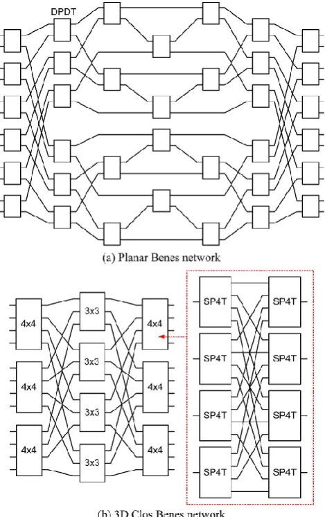
A Benesˇ network is a powerful rearrangeable network with simple control algorithms. Rearrangeable networks mean that any permutation can be statically assigned by re-arranging network paths if necessary. The Benesˇ network is one of the oldest and best-known rearrangeable networks in use for around 40 years. It finds widespread use in shared memory-multiprocessor systems, telecommunication networks, TDMA (Time Division Multiple Access) systems for satellite communications and newer applications such as switching fabrics in internet routers. To realize a RF MEMS switch matrix, the Benesˇ network can be implemented in a planar way. Figure 1a shows the network block diagram for the 12×12 planar Benesˇnetwork using DPDT (Double-Pole Double-Throw) switches. A DPDT switch has two inputs and two outputs. The 12×12 Benesˇnetwork is constructed based on the 16×16 Benesˇnetwork (Chang and Melhem, 1997).
A Clos network is also a subclass of the rearrangeable net-works. Such a network consists of two symmetric outside stages of rectangular switches with an inner stage of square switches. Those three-stage-arranged switch modules are in-terconnected with every module in the adjacent stage by a unique link (Yeh and Feng, 1992). More practical implemen-tation to the RF MEMS switch matrix is 3D Clos-Benesˇ net-work, which is to construct small sub-matrices using SPnT (Single-Pole n-Throw) or DPDT RF MEMS switches and as-semble them to the complicated Clos network as described in Fig. 1b. In the figure, it is depicted that 8 SP4T switches are used to construct a 4×4 switch sub-matrix. For an easy con-nection, the inner stage is 90◦rotated and assembled to the
outer stages in a three-dimensional way.
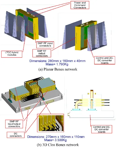
Physically, planar Benesˇand 3D Clos Benesˇnetworks can be realized as Fig. 2. The figure also shows the estimated sizes and weights. The planar Benesˇnetworks consist of sev-eral planar circuit boards. They are simple and easy to assem-ble. They are also robust with compact size. The drawback of the planar Benesˇnetwork is that the isolation can be poor because all circuits in the network are installed in one metal housing. However, the circuit coupling can be suppressed by inserting several metal vias and frames with covers. Com-pared to the planar Benesˇnetwork, 3D Clos Benesˇnetworks have better isolation. They are easier to be extended to the higher order networks. The design of a single sub-matrix is also simple. However, their assembly is mechanically com-plex. As described in the figure, the middle stage is rotated by 90◦and connected to the other stages by several coaxial
ca-bles, which requires high costs and a large footprint together with complex DC control input port connects. The 3D Clos Benesˇnetwork is expected to be bigger and heavier than the planar Benesˇ network’s. In this work, a planar Benesˇ net-work is decided to be fabricated due to its simplicity, smaller footprint and lower weight.
Fig. 1. 12×12 Planar Benesˇand 12×12 3-D Clos Benesˇnetwork.
3 12×12 Switching matrix
3.1 Switching matrix design
Fig. 2. Physical realization of planar Benesˇnetwork and 3-D Benesˇnetwork.
3.1.1 RF connection
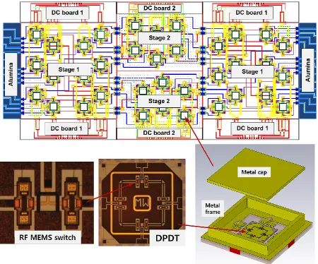
The present 12×12 switch matrix adopts LTCC technology to construct multi-level circuits which enable the RF lines to be crossed without interfering each other. Figure 3 shows the LTCC board layouts which are designed for the 12×12 pla-nar Benesˇ network. For the maximally feasible size of the LTCC board is 8.4cm by 8.4cm, the entire network cannot
146 S. Di Nardo et al.: Design of RF MEMS based switch matrix for space applications
Fig. 3. 12×12 planar Benesˇswitch matrix layout and DPDT switch mount.
Fig. 4. DPDT switch mount on LTCC cavity.
on the LTCC board and electrically isolated from the environ-ment. The DPDT switch is mounted in the deep LTCC cavity, where the switch circuit is located deep further to the level of
the 1st stripline (SL) level on LTCC. The top and bottom layers of the switching element are grounded and connected with several vias. Consequently, each DPDT switch is cap-sulated by grounds and via fences, which suppress coupling between DPDTs. In the RF line design, every horizontal and vertical transition is optimized to have minimum return loss (RL) and insertion loss (IL). Additionally, metal vias are serted between all SLs to suppress line couplings. On the in-put/output sections of the LTCC boards, the alumina boards are located. The reason of using alumina boards is to avoid physical collisions between LTCC boards and RF pin con-nectors on the housing during LTCC board installation.
3.1.2 DC connection
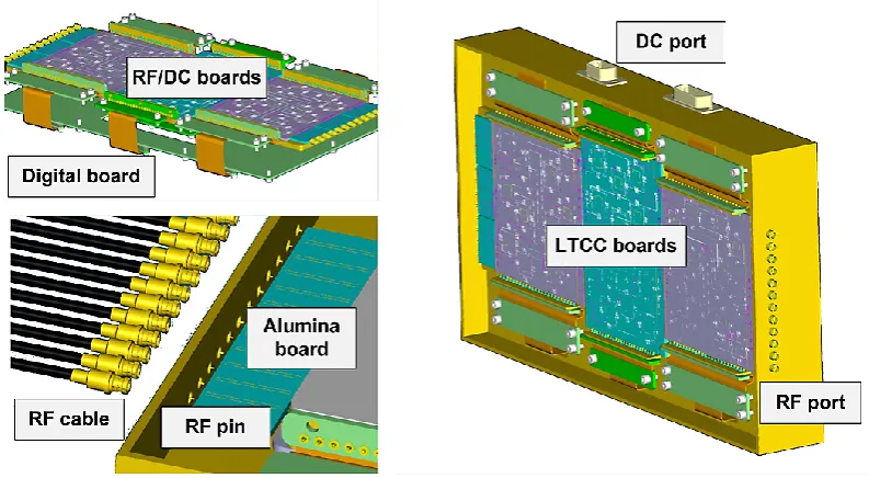
Fig. 5. Physical assembly of 12×12 network.
Fig. 6. Commercially available 12×12 Electromechanical RF Switching System (DowKey Microwave, 2012).
MEMS switches. And 36 DPDT switches are used for the entire network construction. This means, 144 DC contacts should be designed and simultaneously controlled. In this work, the number of DC contacts is decreased by binding DC contact pairs which are commonly activated during op-eration. This can also be done in the DPDT switch level. But the simpler approach is to bind common DC connects in the board level, which is done in the DC board. As a result, the number of DC contacts is reduced to 72.
3.2 Physical assembly
Figure 5 shows the entire physical assembly of the 12×12 switching matrix. RF and DC boards are installed on the metal housing. Under the RF and DC boards, a digital board to generate switch matrix control signals is assembled and connected to the DC ports. The circuits on the RF boards are connected to the RF cables through RF pins. The con-nection between RF board circuits and RF pins are achieved by bond ribbons for high shock and vibration immunity.
As described in Fig. 1, the present switch matrix assembly has a 28cm×12cm×2cm size and a 1.79 kg weight. Fig-ure 6 shows the commercially provided 12×12 mechani-cal switching system (DowKey Microwave, 2012). Its size is 48.3cm×63.5cm×17.8cm and the weight is 38.56 kg. Even after considering it has local control systems and a redun-dant power supply, it is much bigger and heavier than the proposed 12×12 RF MEMS switch matrix.
3.3 Network control
148 S. Di Nardo et al.: Design of RF MEMS based switch matrix for space applications
Fig. 7. Test line select.
Fig. 8. Simulated IL of 12×12 network.
the corresponding switch states are calculated and switch control inputs are generated to be delivered to the digital board in the switch matrix (see Fig. 5). The digital board re-ceives calculated DC inputs and controls high-voltage (typ. 60 V) drivers which practically activate RF MEMS switches.
3.4 RF signal transition performance
Unlike the 16×16 network, the 12×12 network is not sym-metric, which means the number of DPDT switches is dif-ferent according to the path assignment. To simulate the RF signal transition performance, two paths are selected as the best and worst cases in terms of the DPDT switching, layer-to-layer transition number and line lengths. Figure 7 shows the selected paths. Because the network is large and includes
Fig. 9. Simulated RL of 12×12 network.
several complicated transitions, it is difficult to simulate the whole structure by full wave simulators. Therefore the de-tailed transition parts are full wave simulated and their re-sults are combined with circuit simulators. The frequency band definitions are based on the commercial broadcasting satellite up/down link standards, which are L band (1.2-1.8 GHz), S band (2.025-2.3 GHz), C band (3.4-4.2 GHz) and Ku band (10.7-12.75 GHz).
3.4.1 Insertion loss (IL) and Return loss (RL)
Fig. 10. Path coupling cases in the network.
transparent in terms of the RF signal transition. This means ILs should be the same for all connections regardless of the input/output port assignment. In the work, those differences are balanced by inserting resistive materials to the path which has less switching stages compared to the other paths. The re-sistivity and the size are carefully selected not to make severe RL increases. Figure 8 shows that the ILs are well-balanced and below−12 dB up to C band. The main IL contributions are long transmission lines and the high number of switches, which cannot be easily decreased. However, the IL can be compensated by putting amplifiers in the output stage. Gen-erally, high order switch matrices have high linearity ampli-fiers to compensate system IL as the commercially available switch matrix presented in Fig. 6. Concerning RL, the present matrix has some temporal peaks, but in general RL is be-low−15 dB up to Ku band (see Fig. 9). This is better than the commercially available 12×12 mechanical switch
ma-trix which has about−7 dB RL at Ku band (DowKey Mi-crowave, 2012).
3.4.2 Isolation
150 S. Di Nardo et al.: Design of RF MEMS based switch matrix for space applications
Fig. 11. Simulated isolation of 12×12 network.
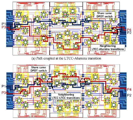
via fences are inserted between lines. A coupling also occurs at the board-to-board transitions, LTCC and LTCC-Alumina. In terms of the worst isolation, the couplings in the board-to-board transitions can be separated into two cases. One case is when the LTCC-Alumina transition ports are two times neighbored (see Fig. 10a). Another case is that LTCC-LTCC transition paths are neighbored and two times coupled (see Fig. 10b). Due to the nature of the Benesˇnetwork, those two cases can not happen at the same time. Figure 11 shows the isolation of the 12×12 network. For all frequency bands of interest, the isolation is better than−50 dB. The commer-cially available 12×12 mechanical switch matrix provided in DowKey Microwave (2012) has a −50 dB input/output isolation, which is comparable to the present matrix isola-tion.
3.4.3 4×4 switch matrix fabrication and measurement
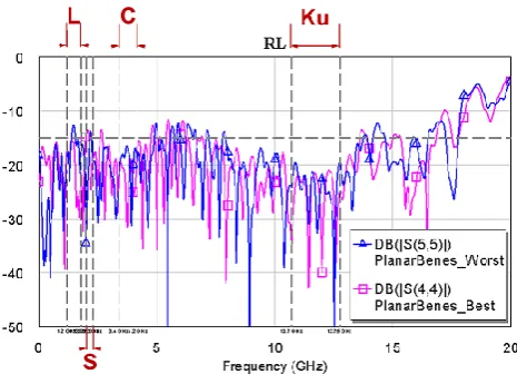
The 4×4 switch matrix in Fig. 12 is to test and verify the design process of the 12×12 switch matrix. The 4×4 ma-trix is the simplified form of the 12×12 matrix and fabri-cated by the same design process and technologies. There are some differences from the 12×12 matrix, which are mainly
Fig. 12. 4×4 switch matrix using RF MEMS switches.
Fig. 13. Measured performance of 4×4 matrix and comparison to the simulations.
4 Conclusions
In this work, a 12×12 switch matrix using RF MEMS and LTCC technologies is designed based on the planar Benesˇ network controlled by Looping algorithms. For the switch-ing components, RF MEMS DPDT switches are used and they are connected by multi-layer transmission lines fabri-cated by LTCC technology. The matrix shows−12 dB IL up to C band and below−15 dB RL up to Ku band. Isolation better than−50 dB is also expected at the frequency bands of interest. Compared to the 12×12 mechanical switch
152 S. Di Nardo et al.: Design of RF MEMS based switch matrix for space applications
Acknowledgements. The work has been carried out in the frame
of the ESA Project No AO/1-5136/06/NL/GLC. The authors will thank Francois Deborgies from ESA/ESTEC for his support and suggestions.
References
Chang, C. and Melhem, R.: Arbitrary Size Benes Networks, J. Par-allel Process. Lett., 7, 279–284, 1997.
Chao, H. J. and Liu, B.: High performance switches and routers, John Wiley & Sons, Inc., Hoboken, New Jersey, USA, 2007.
De Angelis, G., Lucibello, A., Proietti, E., Marcelli, R., Bar-tolucci, G., Casini, F., Farinelli, P., Mannocchi, G., Di Nardo, S., Pochesci, D., Margesin, B., Giacomozzi, F., Vendier, O., Kim, T., and Vietzorreck, L.: RF MEMS ohmic switches for ma-trix configurations, Int. J. Microw. Wirel. Technol., 4, 421–433, doi:10.1017/S1759078712000074, 2012.
Electromechanical – RF Switching System: http://www.dowkey. com, last access: 7 December 2012.
Imanaka, Y.: Multilayered Low Temperature Cofired Ceramics (LTCC) Technology, Springer Science + Business Media, Inc., Boston, USA, 2005.