© 2019, IRJET | Impact Factor value: 7.211 | ISO 9001:2008 Certified Journal
| Page 3741
Bridgeless Boost PFC Rectifier with High Efficiency
S. Venkatesh
1, D. Sarveswararao
2, G.S. Nikhitha
3, Sk. Mehanaz
41
Assistant Professor, KKR&KSR Institute of Technology & Sciences, Guntur
2,3,4Student Member KKR&KSR Institute of Technology & Sciences, Guntur
---***---Abstract
- For the conventional PFC rectifiers, the highefficiency cannot be achieved over a wide input range, and the efficiency will be greatly decreased at low input voltages. In order to overcome the efficiency bottleneck under low line input, a flexible mode bridgeless boost power factor correction (PFC) rectifier is proposed . According to the input voltage, the proposed rectifier can be flexibly adapted to the suitable operating mode to obtain the maximum efficiency. Meanwhile, the circuit components can be reused by different operating modes, so the extra cost is low. In the proposed rectifier, a back-to-back bridgeless boost PFC topology is adopted at high line conditions and a three-level bridgeless boost PFC topology is rebuilt to reduce the switching losses at low line conditions. Compared with the traditional bridgeless boost PFC rectifier, an extra low-voltage bidirectional switch (usually composed of two switches) is added, so the increased cost is low. In addition, the low common mode noise can be achieved at both high and low line conditions due to the direct connection between the input mains and the output electrolytic capacitor. The detailed principle analysis about the proposed rectifier is presented in this paper. Finally, an experimental prototype is built to verify the feasibility and the effectiveness of the proposed topology
Key Words: bridgeless PFC, flexible mode, high effi-ciency, low common mode noise.
1. INTRODUCTION
In order to meet the harmonic regulations and standards, such as the power supplies with active power factor correction (PFC) feature are required for various types of electronic equipment. Meanwhile, the increasing requirements of high efficiency have been forcing the designers to look for any potential opportunities to reduce the converter losses. The most common solution is the conventional PFC rectifier which is widely used for various kinds of computers, workstations, servers and so on. However, it suffers from high conduction losses since the input current always flows through two bridge diodes and a power switching device. Besides, the efficiency decrease caused by conduction losses is more obvious when the input line voltage is low, which usually leads to low power density since a large heat sink is needed. In order to overcome the shortcomings of the conventional PFC converter
1.1 Traditional full bridge PFC rectifier
[image:1.595.355.526.325.412.2]The key principle that drives the boost converter is the tendency of an inductor to resist changes in the current. When being charged it acts as a load and absorbs energy (somewhat like a resistor); when being discharged it acts as an energy source (somewhat like a battery). The voltage it produces during the discharge phase is related to the rate of change of current, and not to the original charging voltage, thus allowing different input and output voltages.The traditional full bridge rectifier is shown in fig1.1
Fig 1.1 Traditional full bridge PFC rectifier The Power factor correction using boost converter can be used to attain a decent power factor along with some advantages such as higher output voltage, light and less bulky as compared to capacitor banks used for PFC, the output voltage can be stepped down as per the requirement using chopper circuit preceding the PFC circuit.
1.2 Dual boost bridgeless PFC rectifier
In these boost bridgeless PFC rectifiers, the most practical and potential to-pologies are the dual-boost bridgeless PFC rectifier (DBBL PFC) shown in Fig.1.2 and the back-to-back bridgeless PFC rectifier (BTBBL PFC) shown in Fig. 1.3.
[image:1.595.337.537.608.744.2]
© 2019, IRJET | Impact Factor value: 7.211 | ISO 9001:2008 Certified Journal
| Page 3742
Since both of them have lower common mode (CM) noiseinterference and better reliability compared with the others. Nevertheless, it can be noted that the magnetic core utilization is low for the DBBL PFC rectifier. Although a multiple-winding, multicore inductor can be used to improve the utilization of the magnetic material , the efficiency of the rectifier is also reduced, which is not expected. For the above two rectifiers, the high efficiency can be achieved when the input voltage is high (rating value is 220~240 Vrms). If the input voltage decreases, the total conduction and switching losses although are reduced than the topology shown in Fig.1.1, however are still high with the in-crease of input current, the efficiency under low input voltages is still much lower than that under high input voltages.
It seems to be much difficult to further reduce the conduction losses for the bridgeless PFC rectifiers, so many bridge-less PFC rectifiers have been modified to improve the efficiency via soft switching techniques. According to the ways of realizing soft switching, these modified PFC rectifiers can be divided into several groups.
[image:2.595.312.555.216.336.2]1.3 Symmetrical back to back bridgeless boost pfc
rectifier
Fig.1.3 Symmetrical back to back bridgeless boost pfc rectifier
[image:2.595.327.515.385.506.2]The figure of symmetrical back to back bridgeless boost PFC rectifier is shown in fig.1.4. In order to overcome the shortcomings of the conventional PFC converter, many researchers have made great efforts to develop the bridgeless boost PFC rectifiers which can achieve higher efficiency by reducing the number of power components in the line current path.
Fig.1.4 Symmetrical back to back bridgeless boost PFC rectifier
In these boost bridgeless PFC rectifiers, the most practical and potential topologies are the dual-boost bridgeless PFC rectifier (DBBL PFC) shown in Fig.1.2 and the back-to-back bridgeless PFC rectifier (BTBBL PFC) shown in Fig 1.3 since both of them have lower common mode (CM) noise interference and better reliability compared with the others.
1.4 Improved three level boost pfc rectifier
Fig 1.5 Improved three level boost pfc rectifier
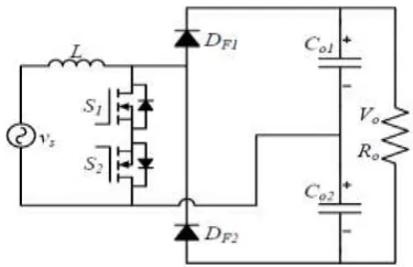
[image:2.595.50.275.395.528.2]1.5 Three level bridgeless boost pfc rectifier
Fig 1.6 Three-level bridgeless boost PFC rectifier The bridgeless configuration topology avoids the need for the rectifier input bridge yet maintains the classic boost topology. This is easily done by making use of the intrinsic body diode connected between drain and source of Power MOS switches. Fig.1.6 shows the topology of a three-level bridgeless boost PFC rectifier (TLBL PFC), whose structure is simple. First, there are fewer semiconductor components in the current path. When the bidirectional switch 𝑆1𝑆2 is turned off, there is only one fast diode to carry
the current in the TLBLPFC, while two diodes in the BTBBL PFC and DBBL PFC.
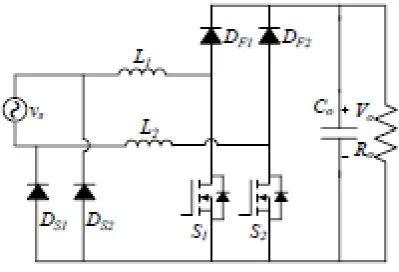
2. FLEXIBLE MODE BRIDGELESS BOOST PFC
RECTIFIER
The proposed figure of Flexible mode bridgeless boost PFC rectifier is shown above. An AC supply voltage Vs is given as input. An inductor L is connected to the input. It consists of two power MOSFET S1,S2 and two auxiliary
[image:2.595.48.277.628.751.2]© 2019, IRJET | Impact Factor value: 7.211 | ISO 9001:2008 Certified Journal
| Page 3743
slow diodes DS1,DS2.Two output capacitors Co1,Co2 arepresent followed by a resistive load at the end.
[image:3.595.305.566.55.277.2]There are usually two typical line voltages (100~120 Vrms and 220~240 Vrms) around the world.
Fig 2.1 Flexible mode bridgeless boost PFC rectifier
The proposed FMBL PFC can be simply treated as two independent boost PFC circuits according to the line voltage. If the line voltage is within the range of 100~120 Vrms, the bidirectional switch S3S4 is turned on, the FMBL
PFC is adapted to a TLBL PFC (referred as “TLBL mode”) which can promote the efficiency by reducing the switching losses. If the line voltage is within the range of 220~240 Vrms, the bidirectional switch S3S4 is always turned off.
Therefore, the proposed FMBL PFC is the same as the BTBBL PFC (referred as “BTBBL mode”)
When the bidirectional switch 𝑆1𝑆2 is turned off, the
inductor releases its stored energy to the output capacitors 𝐶𝑜1, 𝐶𝑜2 and the load resistor 𝑅𝑜 through the bridge diodes 𝐷𝐹1 and 𝐷𝑆1.
3 SIMULATION ANALYSIS
[image:3.595.50.281.147.294.2]3.1 AC-DC Converter without boost PFC
Fig. 3.1 AC-DC converter without boost PFC rectifier
Fig.3.2 Input voltage and current waveforms of AC-DC rectifier without boost rectifier
[image:3.595.308.562.425.588.2]Fig 3.2 shows the input voltage and current waveforms of AC-DC rectifier without boost pfc rectifier. After simulation, The output waveforms of AC-DC rectifier without C filter can observed below in Fig 3.3. An input of 230V AC supply is given as input an output of 228V is obtained. As this model is without boost PFC, Capacitor is not present. The output voltage and current waveforms are observed in Fig 3.3.
Fig 3.3 Output voltage and current waveforms of AC-DC rectifier without boost pfc
The Fig 3.3 shows the output voltage and current waveforms of AC-DC rectifier without boost pfc. The output voltage observed in the waveform is 228V. The output current observed is 22.8A.
3.2 AC-DC Converter with C filter & without PFC
[image:3.595.42.284.574.730.2]© 2019, IRJET | Impact Factor value: 7.211 | ISO 9001:2008 Certified Journal
| Page 3744
and distortions produced in the output are removed with the [image:4.595.47.302.143.279.2]help of the Filter.
Fig 3.4 AC-DC converter with C filter
Fig 3.5 Input current and voltage waveforms of AC-DC rectifier with C filter
[image:4.595.37.558.151.663.2]After simulation of the circuit (Fig 3.4),The obtained output current and voltage waveforms are shown in Fig 3.6.
Fig 3.6 Output current and voltage waveforms of AC-DC rectifier with C filter
3.3Three level bridgeless boost PFC rectifier
The simulink model of Three level bridgeless boost PFC rectifier is shown in Fig 3.7.The input and output waveforms obtained are shown in Fig 3.8,3.9.
Fig. 3.7 Three level bridgeless boost PFC rectifier.
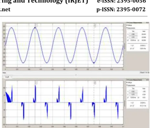
Fig 3.8 Input current and voltage waveforms for Three level bridgeless boost PFC rectifier
[image:4.595.40.557.524.709.2]© 2019, IRJET | Impact Factor value: 7.211 | ISO 9001:2008 Certified Journal
| Page 3745
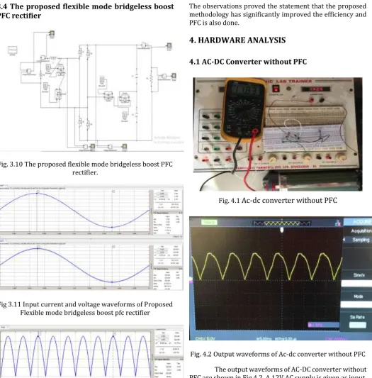
3.4 The proposed flexible mode bridgeless boost
[image:5.595.41.567.91.625.2]PFC rectifier
Fig. 3.10 The proposed flexible mode bridgeless boost PFC rectifier.
Fig 3.11 Input current and voltage waveforms of Proposed Flexible mode bridgeless boost pfc rectifier
Fig 3.12: Output current and voltage waveforms for proposed flexible mode bridgeless boost PFC rectifier.
The observations proved the statement that the proposed methodology has significantly improved the efficiency and PFC is also done.
4. HARDWARE ANALYSIS
4.1 AC-DC Converter without PFC
Fig. 4.1 Ac-dc converter without PFC
Fig. 4.2 Output waveforms of Ac-dc converter without PFC
The output waveforms of AC-DC converter without PFC are shown in Fig 4.2. A 12V AC supply is given as input.
4.2 Traditional boost pfc rectifier
© 2019, IRJET | Impact Factor value: 7.211 | ISO 9001:2008 Certified Journal
| Page 3746
Traditional full bridge boost PFC can do power factor correct [image:6.595.294.559.55.255.2]but cannot improve the efficiency effectively.
Fig. 4.3 Output voltage waveform of traditional full bridge boost PFC
4.3 Proposed flexible mode Bridgeless boost PFC
rectifier
[image:6.595.37.290.128.266.2]Fig.4.4 Proposed flexible mode Bridgeless boost PFC rectifier
[image:6.595.36.288.352.513.2]Fig.4.5 Input voltage waveforms of proposed bridgeless boost PFC rectifier
Fig. 4.6 Output voltage waveform of proposed bridgeless boost PFC rectifier
3. CONCLUSIONS
The output response of a Boost PFC converter for power factor correction and efficiency improvement has been simulated. The simulated result is studied and this work showed an increase in efficiency over a wide range of input voltage. The proposed topology reduces the extra cost and complexity of the circuit. The simulation shows this improves the power factor. The improvement in power factor and decrement in distortion are clearly observed.The simulation of proposed method is done in MATLAB and various waveforms are observed justifying that the power factor is corrected and efficiency of the rectifier is increased for a wide range of input voltage. The results are stated after comparing the previous and traditional methods.
The Hardware is done over a wide range of voltage with filter to reduce the harmonics produced and increase efficiency as a result. The Hardware results also justify the increase in the efficiency and improvement of power factor.
REFERENCES
[1] Limits-Limits for Harmonic Current Emissions
(Equipment Input Cur-rent ≤ 16 A per Phase), IEC 61000-3-2, 2010, EMC Part 3-2
[2] J. Sun, “Input impedance analysis of single-phase PFC
converters,”IEEE Trans. Power Electron., vol. 20, no. 2, pp. 308-314, Mar. 2005.
[3] R. Martinez and P. N. Enjeti, “A high-performance
single-phase rectifier with input power factor correction,” IEEE Trans. Power Electron., vol. 11, no.2, pp. 311–317, Mar. 1996
[4] J. W. Lim and B. H. Kwon, “A power-factor controller for
single phase PWM rectifiers,” IEEE Trans. Ind. Electron., vol. 46, no. 5, pp. 1035– 1037, Oct. 1999.
[5] B. Singh, B. N. Singh, A. Chandra, K. Al-Haddad, A.
[image:6.595.36.288.559.686.2]© 2019, IRJET | Impact Factor value: 7.211 | ISO 9001:2008 Certified Journal
| Page 3747
improved power quality AC-DC converters,” IEEE Trans.Ind. Electron., vol. 50, no. 5, pp. 962-981, Oct. 2003.
[6] W.-Y. Choi, J.-M. Kwon, E.-H. Kim, J.-J. Lee, and B.-H.
Kwon,“Bridgeless boost rectifier with low conduction losses and reduced di-ode reverse-recovery problems,” IEEE Trans. Ind. Electron., vol. 54, no. 2, pp. 769–780, Apr. 2007.
[7] L. Huber, Y. Jang, and M. M. Jovanovic, “Performance
evaluation of bridgeless PFC boost rectifiers,” IEEE Trans. Power Electron., vol. 23, no. 3, pp. 1381-1390, May. 2008.
[8] Y. Jang and M. M. Jovanovic, “A bridgeless PFC boost
rectifier with optimized magnetic utilization,” IEEE Trans. Power Electron., vol. 24, no. 1, pp. 85-93, Jan. 2009.
[9] J. Zhang, B. Su, and Z. Lu, “Single inductor three-level
bridgeless boost power factor correction rectifier with nature voltage clamp,” IET Power Electron., vol. 5, no. 3, pp. 358-365, Mar. 2012.
[10] Y.-S. Kim, W.-Y. Sung, and B.-K. Lee, “Comparative
performance analysis of high density and efficiency PFC topologies,” IEEE Trans.
BIOGRAPHIES
S. Venkatesh received M.tech (Power Electronics) From jntu, anantapur, A.P , India (2012 – 2014). He is currently working as Assistant Professor in the department of EEE at KITS Guntur Dist, A.P , India. His research areas include Power Electronics and Electric Drives.
D.Sarveswararao pursuing B.Tech (EEE) in KITS , Guntur. His research areas include Power Electronics and Electric Drives.
G.S.Nikhitha pursuing B.Tech (EEE) in KITS , Guntur. Her research areas include Power Electronics and Electric Drives.