Design and Comparison of Low Power High
Performance Online Testable Combinational
Circuits with Different Reversible Logic Gates
Ranjusha K
#1, Remya K P
*2, Salmanul Faris
#3#1M Tech VLSI Student, Dept Of Electronics & Communication, NCERC, Pambadi, Thrissur, Kerala, India. *2
Asst Professor. Dept Of Electronics & Communication, NCERC, Pambadi, Thrissur, Kerala, India
#3 Engineer KECL, Kuttipuram, Kerala, India.
Abstract —In current scenario, the reversible logic design attracting more interest due to its low power consumption. Reversible logic is very important in low-power VLSI design,quantum computing, nanotechnology and optical computing. In this paper, a new 4*4 reversible gate termed OTG (Online Testable Gate) and CTSG are proposed suitable for online testability in reversible logic circuits. OTG can also work singly as a reversible full adder with a bare minimum of two garbage outputs. OTG is shown better than the recently proposed R1 gate (introduced for providing online testability in reversible logic circuits), in terms of computation complexity. The proposed reversible gate is combined with the existing 4*4 Feynman gate to design online testable reversible adders such as ripple carry adder, carry skip adder and BCD adder and 4*1 Multiplexers and De Multiplexers. The important reversible gates used for reversible logic synthesis are Feynman Gate, Fredkin gate, toffoli gate, New Gate, DKG Gate and peres gate etc. The proposed system is the design of basic reversible gate and comparison of leakage power, dynamic power, total power. The testable reversible circuits proposed in this work are shown to be better than the recently proposed testable designs in terms of number of reversible gates, garbage outputs and unit delay.The reversible logic circuits are designed and implemented using VHDLcode. The synthesize and simulation results are obtained in Xilinx ISE version 10.1i and MODEL SIM 6.4a.
Keywords — Garbage outputs, Online Testable Gate(OTG), Power consumption, Reversible logic circuits, CTSG, Feynman Gate, Fredkin gate, Toffoli gate, DKG Gate, Peres Gate and Xilinx ISE version 10.1i and MODEL SIM 6.4a.
I. INTRODUCTION
Energy loss, is an important consideration in a binary arithmetic circuit. Part of the problem of energy dissipation is related to non-ideal of transistors and materials. Higher level of integration and the use of new fabrication processes have reduced the heat loss over the last decades. Another problem arises from Landauer‟s principles [1] state that, logic computations that are not reversible,
necessarily generate heat KTln2 for every bits of information that is lost, where K is the Boltzmann‟s constant and T is the temperature. Reversible are circuits (gates) in which there is a one-to-one mapping between vectors of inputs and outputs. The reversible designs do not lose any information.. Bennett showed that kTln2 energy dissipation would not occur, if a computation is carried out in a reversible way [2], since the amount of energy dissipated in a system bears a direct relationship to the number of bits erased during computation... These circuits can generate unique output vector from each input vector, and vice versa, that is, there is a one-to-one mapping between input and output vectors.
II. LITERATURESURVEY
Many of the authors have been discussed about reversible computing techniques. A wide range of online testable reversible techniques and methods have been used in the conventional times and even in the recent past years. Irreversibility and heat generation in the computing process[1]Landauer, R proposed that computing machines inevitably involve devices which perform logical functions that do not have a single-valued inverse. This logical irreversibility is associated with physical irreversibility and requires a minimal heat generation, per machine cycle, typically of the order of kT for each irreversible function. This dissipation serves the purpose of standardizing signals and making them independent of their exact logical history.
Testability[4] Dilip P. Vasudevan , Parag.K. Lala and J.Patrick. Parkerson proposed that Conventional digital circuits dissipate a significant amount of energy because bits of information are erased during the logic operations. Thus, if logic gates are designed such that the information bits are not destroyed, the power consumption can be reduced dramatically. The information bits are not lost in case of a reversible computation. This has led to the development of reversible gates. This paper proposes three new reversible logic gates; two of the proposed gates can be employed to design online testable reversible logic circuits.
III.BASIC DEFINITIONSOFREVERSIBLE GATESANDTHEIRPROPERTIES
In this section, we have represented the basic ideas and definitions some of the properties of reversible logic. Quantum realizations of those properties have been also illustrated in this section
.
A. Reversible Gate
It is an n input, n output circuit that produces a unique output pattern [6] for each possible input pattern (one-to-one correspondence relation). For an n×n reversible gate if the input vector be Iv and the output vector Ov then Iv = (I1, I2, I3…In) and Ov=(O1,O2,O3…On), respectively. The relationship between them is denoted as (Iv ↔Ov).
B. Online Testability
According to there are two type of testing which one of this is online (concurrent testing) and another is offline (non concurrent testing), or both can be combined. Online testing is working while the system is performing its normal operation, allowing faults to be detected in real time. Offline testing requires the system or a part of the system to be taken out of operation to perform testing, and generally involves the application of a set of test vectors that will detect all possible faults under a given fault model (a complete test set).
C. Quantum Cost
Quantum cost can be computed by substituting the reversible gates of a circuit by a cascade of elementary quantum gates. Elementary quantum gates realize quantum circuit that are inherently reversible and manipulate qubits.
D. GarbageOutput
Unwanted or unused outputs of a reversible gate which are not used as the input of other reversible gates, are known as garbage outputs. Garbage outputs are needed only to maintain reversibility. Heavy price paid off for each garbage output. The calculation of garbage output can be changed in case of using that gate in different digital circuits. The Feynman gate produces one garbage output.
E. Constant Input
Sometimes it is needed to apply constant input to any reversible gate for a specific logic operation. Constant input means either 0 or 1. In reversible circuit to minimize constant inputs because it may cause delay.
IV.BACKGROUND STUDY OF EXISTING
REVERSIBLE ONLINETESTABLEFULL ADDERS
In this project, the focus is on the proposal of a new 4*4 reversible gate termed ―OTG‖ (Online Testable Gate), and its use in designing efficient online testable reversible adder circuits. The OTG can work singly as a reversible full adder .The used OTG gate is combined with 4*4 FEYNMAN gate [5,6] to provide the online testability feature. The testable 1-bit reversible full adder designed using the used reversible OTG gate, is shown to be better than the recently used testable full adder used in terms of number of reversible gates, garbage outputs and unit delay. The used OTG gate is used to design online testable reversible adders such as ripple carry adder, carry skip adder and BCD adder. The testable reversible BCD adder is presented first time in literature. The online testable reversible circuits used and designed in this work will form the basis for a testable primitive reversible/quantum ALU.
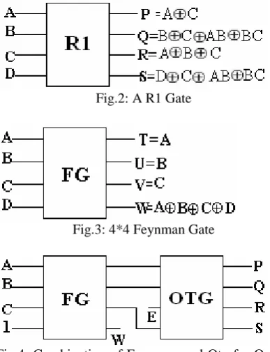
Figure 1 shows the used OTG gate. OTG can also implement all Boolean functions. The implementation of OTG gate for realizing NAND function. Since, NAND is a universal gate any Boolean function can be realized with OTG gate. The used OTG gate is more efficient in computation complexity, compared to recently used 4*4 ―R1‖gate [9] (R1 gate is shown in Fig.2. and was used for introducing online testability in reversible logic circuits). Figure 2.b shows the working of OTG as a reversible full adder with bare minimum of two garbage outputs (at least two garbage outputs will be required to realize a reversible full adder).
A. Used New Gate
In this project, we propose a novel 4*4 reversible gate termed ―OTG‖ (Online Testable gate) and CTSG which are suitable for providing online testability in reversible logic circuits.
Fig.2: A R1 Gate
Fig.3: 4*4 Feynman Gate
Fig.4: Combination of Feynman and Otg for Online Testability
Fig.5: Combination of Feynman and Otg termed ‗CTSG‘
Fig. 5 shows the realization of the used CTSG block as an online testable reversible full adder with the complementary R & W outputs (input E=0 in this case).
Fig. 6: Ctsg as a Reversible Full Adder with Online Testability
B. Design of Online Testable Reversible Adders
The used CTSG block (OTG and FEYNMAN gate) is used to design efficient online testable reversible arithmetic adders. The online testable reversible adders designed in this work are ripple carry adder, carry skip, and BCD adder and Multiplexer and De Multiplexers.
B.1 Reversible Design of Ripple Carry Adder using CTSG
The full adder is the basic building block in a ripple carry adder. The reversible online testable ripple carry adder can be designed by cascading the one bit testable reversible full adder designed from CTSG block as shown in Fig.7. Thus, we are able to achieve the improvement ratio of 8, 1.5 and 8 in terms of number of reversible gates, garbage outputs and unit delay, respectively.
Fig. 7: Online Testable Reversible Ripple Carry Adder
.
V. DESIGN OF ONLINE TESTABLE MULTIPLEXER
AND DE MULTIPLEXER
A. Design of a 4 in To 1 Multiplexer
A Multiplexer is a combinational circuit that is given a certain number (usually a power of two) data inputs, let us say 2n, and n address inputs used as a binary number to select one of the data inputs. The Multiplexer has a single output, which has the same value as the selected data input. In other words, the Multiplexer works like the input selector of a home music system. Only one input is selected at a time, and the selected input is transmitted to the single output. The truth table for a Multiplexer and the corresponding logic diagram were shown below.
TABLEI
TRUTHTABLEFORA4INTO1 MULTIPLEXER
INPUTS SELECT LINES OUTPUT
S0 S1 Z
A 0 0 A B 0 1 B C 1 0 C D 1 1 D
Fig.8: Logic Diagram For A 4 Into 1 Multiplexer. The design of a 4 in to 1 Multiplexer can be well defined also using the suggested online testable gate. Using the truth table of the CTSG gate and also the inputs and outputs of the CTSG gate, we can design a 4 * 1 mux very easily in a simple structural VHDL model. As we are going to use CTSG gate in the implementation of the mux, the online testable feature of the CTSG gate also imparts to the mux design. So finally a online testable Multiplexer is also designed.
B. Design of an Online Testable 1 To 4 Demultiplexer
The Demultiplexer is the inverse of the Multiplexer, in that it takes a single data input and n address inputs. It has 2n outputs.
TABLEIII
TRUTHTABLEFORADEMULTIPLEXER Data Address Outputs
S1 S0 Y0 Y1 Y2 Y3
D 0 0 D 0 0 0 D 0 1 0 D 0 0 D 1 0 0 0 D 0 D 1 1 0 0 0 D
A Demultiplexer (DMUX) is a device which essentially performs the opposite operation to the MUX..The conventional Demultiplexer 1:4 logic diagram and its truth table were shown below. Here data is the input to the Demultiplexer, s1 and s0 are the select lines, y0, y1, y2, y3 are the output lines.
Fig.9: Logic Diagram For A 1 To 4 Demultiplexer. The design of a 1*4 Demultiplexer can be well defined also using the suggested online testable gate. Using the truth table of the CTSG gate and also the inputs and outputs of the CTSG gate, we can design a 1 * 4 demux very easily in a simple structural VHDL model. As we are going to use CTSG gate in the implementation of the demux , the online testable feature of the CTSG gate also imparts to the demux design. So finally a online testable Demultiplexer is also designed using the CTSG gate.
VI.PROPOSEDSYSTEM
The information bits are not lost in case of a reversible computation. This has led to the development of reversible gates. This paper proposes four new reversible logic gates; one of the proposed gates can be employed to design online testable reversible logic circuits.
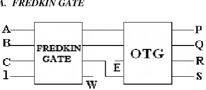
A. FREDKIN GATE
Fig.10: Combination of Fredkin and Otg for Online Testability
Fig.10 shows a 3*3 Fredkin gate. The input vector is I (A, B, C) and the output vector is O (P, Q, R). The output is defined by P=A, Q=A′BAC and R=A′CAB. Quantum cost of a Fredkin gate is 5.
Fig.11: Fredkin Gate
TABLEIIIIITRUTH TABLE OF FREDKIN GATE
A B C P Q R
0 0 0 0 0 0 0 0 1 0 0 1 0 1 0 0 1 0 0 1 1 0 1 1 1 0 0 1 0 0 1 0 1 1 1 0 1 1 0 1 0 1 1 1 1 1 1 1
B. TOFFOLI GATE
Fig.11 shows a 3*3 Toffoli gate. The input vector is I (A, B, C) and the output vector is O(P,Q,R). The outputs are defined by P=A, Q=B, R=ABC. Quantum cost of a Toffoli gate is 5.
Fig.12: Toffoli Gate
Fig.13: Combination of Toffoli Gate and Otg for Online Testability
TABLEIVVTRUTH TABLE OF TOFFOLI
GATE
A B C P Q R
0 0 0 0 0 0 0 0 1 0 0 1 0 1 0 0 1 0 0 1 1 0 1 1 1 0 0 1 0 0 1 0 1 1 0 1 1 1 0 1 1 1 1 1 1 1 1 0
C. DKG GATE
A 4*4 reversible DKG gate that can work sigly as a reversible Full adder and Full subtractor. If input A=0,the proposed gate works as a reversible Full adder,and if input A=1,then it works as a reversible Full subtractor. DKG GATE is shown in fig.
Fig.14: Combination of Dkg Gate and Otg for Online testability
A B C D P Q R S
0 0 0 0 0 0 0 0 0 0 0 1 0 0 0 1 0 0 1 0 0 1 0 1 0 0 1 1 0 1 1 0 0 1 0 0 1 0 0 1 0 1 0 1 1 0 1 0 0 1 1 0 1 1 1 0 0 1 1 1 1 1 1 1 1 0 0 0 0 1 0 0 1 0 0 1 0 0 1 1 1 0 1 0 0 1 1 1 1 0 1 1 0 0 1 0 1 1 0 0 1 1 0 1 1 1 0 1 1 0 0 0 1 1 1 0 1 1 0 0 1 1 1 1 1 0 1 1
D. PERES GATE
Fig.15: Peres Gate
Fig.16: Combination of Peres Gate and Otg for Online testability
TABLEVTRUTH TABLE OF PERES GATE
A B C P Q R
0 0 0 0 0 0 0 0 1 0 0 1 0 1 0 0 1 0 0 1 1 0 1 1 1 0 0 1 1 0 1 0 1 1 1 1 1 1 0 1 0 1 1 1 1 1 0 0
In order to design a OTG combination with different reversible gate circuits, few conditions of reversible circuit designing are to be considered which are (a) There must be no feedback. (b) There must be no fan-out. (c) Garbage outputs must be minimum. (d) Total number of gates must be minimum.
A logic synthesis technique using a reversible gate should have the following features:
use a minimum number of garbage outputs use a minimum input constants
use a minimum circuit level use a minimum number of gates
TABLEVI RESULTSOFCOMPARISON OFMEMORYANDDELAY
Types of Gates
Power (W)
Slice Register
Delay (ns)
Memory (kb)
Peak Memory
Usage (mb) Feynman
Gate .20628 1/14752 6.209 211180 135
Fredkin
Gate .20486 1/14752 6.2 211180 135
Toffoli
Gate .20553 1/14752 6.236 211181 134
Peres
Gate .20541 1/14752 6.32 211180 135
Dkg
Gate .20629 2/14752 6.32 212204 135
Fig.17: Output Waveform of DKG Gate
Fig.18: Output Waveform of Fredkin Gate
Fig.19: Output Waveform of Peres Gate
VII.CONCLUSION
The project implements low power high performance online testable combinational circuits with different reversible logic gates. Four new reversible logic gates have been proposed in this paper. Each one these gates can be paired such that any function implemented using the gate pair will be online testable gate(OTG). The most important requirement of the reversible gate-based design is the reduction of garbage outputs rather than the actual number of gates. The important reversible gates used for reversible logic synthesis are Feynman Gate, Fredkin gate, toffoli gate, DKG Gate and peres gate etc. The proposed system is the design of basic reversible gate and comparison of leakage power, dynamic power, total power. The testable reversible circuits proposed in this work are shown to be better than the recently proposed testable designs in terms of number of reversible gates, garbage outputs and unit delay. The reversible logic circuits are designed and implemented using VHDL code. The synthesize and simulation results are obtained in Xilinx ISE version 10.1i and MODEL SIM 6.4a..
TABLEVIII DISCUSSIONOF PARAMETERS
PARAMETER RCA CSA BCD MUX DEMUX
Power Consumption(m w)
50 50 50 92 92
Memory
Occupied(kb) 100652 100652 100652 99628 99628
Combinational
Time Delay(ns) 12.38 12.40 13.764 8.137 7.85
In future, the work can be extended upto the design of an ALU which is also online testable. The power dissipation, power utilization, unit time delay and others can be optimized to a level so that this can replace the conventional ALU used in present days.
Acknowledgment
For the successful completion of this project, I thank Salmanul Faris, Engineer, KECL, Kuttippuram, India for providing the resources to carry out the project.
I thank my guide Remya K.P, Assistant Professor in Department of Electronics and Communication
Engineering, NCERC, Pampady, India for providing valuable suggestions during the project.
I thank all my guides, family members and friends who helped me directly or indirectly during this work.
References
[1] Landauer, R., 1961. Irreversibility and heat generation in the computing process. IBM J. Res. Develop., 5: 183-191. [2] C.H. Bennett, ―Logical Reversibility of Computation‖,
IBM J.Research and Development, 17, 525 (1973). [3] D.P. Vasudevan , P.K. Lala and J.P. Parkerson, ―Online
Testable Reversible Logic Circuit Design using NAND Blocks‖, Proc, Symposium on Defect and Fault Tolerance, October 2004, pp-324-331.
[4] D. P. Vasudevan, P. K. Lala, J. P Parkerson, ―Reversible-Logic Design With Online Testability‖, IEEE Transactions on Instrumentation and Measurement, VOL. 55, NO. 2, pp. 406-414, APRIL 2006.
[5] E. Fredkin, T Toffoli, ―Conservative Logic‖, International Journal of Theor. Physics, vol. 21, nos. 3-4, pp. 219-253, 1982.
[6] T. Toffoli., ―Reversible Computing‖, Tech memo MIT/LCS/TM-151, MIT Lab for Computer Science (1980). [7] K. N. Patel, J. P. Hayes, and I. L. Markov, ``Fault Testing for Reversible Circuits'', IEEE Trans. on CAD, 23(8), pp. 1220-1230, August 2004.
[8] P.O. Boykin and V.P. Roychowdhury, "Reversible fault-tolerant logic" Proceedings International Conference on Dependable Systems and Networks, 2005 ( DSN 2005), 28 June-1 July 2005.
[9] Avishek Bose, Hafiz Md. Hasan babu, Shalini Gupta, Design of Compact Reversible Online Testable Ripple carry order” IEEE WIECON-ECE Dec 2015.
[10] Nagarjun S, Nagendra R, Kiran N, Kiran Kumar K N, Designand Comparison of Reversible and Irreversible Sequential Logic Circuits, IJRAET, Volume-2, Issue -4, 2014.
[11] B.Raghu kanth, B.Murali Krishna, M. Sridhar, V.G. Santhi Swaroop ―A DISTINGUISH BETWEEN REVERSIBLE AND CONVENTIONAL LOGIC GATES ‖, International Journal of Engineering Research and Applications (IJERA) ISSN: 2248-9622 www.ijera.com Vol. 2, Issue 2,Mar-Apr 2012, pp.148-151
[12] Raghava Garipelly, P.Madhu Kiran, A.Santhosh Kumar ―A Review on Reversible Logic Gates and their Implementation‖ International Journal of Emerging Technology and Advanced Engineering Website: (ISSN 2250-2459, ISO 9001:2008 Certified Journal, Volume 3, Issue 3, March 2013)
[13] Punam Prabhakar Bhalerao,Sameena Zafar ―New Design For Obtain Fault Tolerant Logic Gate Using Quantum –Dot Cellular Automata‖ International Journal of Science and Research (IJSR) Volume 3,Issue 7,July 2014
[14] A COMPARITIVE STUDY OF REVERSIBLE LOGIC
GATES, International Journal of VLSI & Signal Processing Applications, Vol.2,Issue 1, Feb 2012, (51-55), ISSN 2231-3133.