e-ISSN: 2250-3021, p-ISSN: 2278-8719 Vol. 3, Issue 4 (July. 2013), ||V1 || PP 38-43
Three Level Three Phase Cascade Dual-Buck Inverter With
Unified Pulsewidth Modulation
Aswathi M.
1, S.Anusha
21. P.G scholar, Francis Xavier Engineering College, Tirunelveli. 2. Assistant professor, Francis Xavier Engineering College, Tirunelveli.
Abstract:- This paper presents a three phase voltage source dual buck inverter using unified PWM technique. This technique enhances the system reliability. It is a hard switching voltage source inverter. This topology uses power MOSFET as the active device and as a result it has lower switching losses and it can be designed at higher switching frequencies to reduce current ripple and size of passive components. The unified PWM technique reduces the computational burden in real time implementations by making use of a digital signal processor. Different PWM methods like Sinusoidal PWM, Space Vector PWM and Discontinuous Space Vector PWM (DSVPWM) can be applied to a three phase dual buck inverter. It does not need dead time and has no shoot through concerns. A three level cascaded dual buck inverter is also controlled using unified PWM technique.
I. INTRODUCTION
The standard half-bridge or full-bridge inverter is a typical voltage source inverter (VSI) with two active switches in one phase leg. It needs dead time to prevent shoot-through problems between the switches in one leg. Because of dead time effect, the output waveforms can be distorted and the equivalent transferred energy of pulse-width modulation (PWM) is reduced. At some fault conditions, even with added dead time, shoot-through is still the reason for dominant failure of the circuit. In addition, with higher dc bus voltage operation, this standard inverter cannot simply employ power MOSFETs as the active switches due to the reverse recovery problem of the body diode of MOSFETs.
To utilize the benefits of power MOSFETs, such as lower switching loss, resistive conduction voltage drop, and fast switching speed which reduces the current ripple and the size of passive components, the dual buck inverter had been proposed. The dual-buck inverter typically consists of two buck inverters with one operating at the positive half-cycle while the other one working at the negative half-cycle. The dual-buck type inverters do not need dead time, and they totally eliminate the shoot-through concerns, thus leading to greatly enhanced system reliability. It can be hard switched because the body diode of MOSFET never conducts, and the external diodes can be independently selected to minimize switching losses.
This paper proposes a three level cascaded dual buck inverter in which two three-phase dual-buck inverter shown in Fig. 1 are connected in series.. It is hard-switching-based, but it can incorporate power MOSFETs as the active switches. The number of switches is the same as that of the standard three-phase voltage source inverter using insulated-gate-bipolar-junction-transistors (IGBTs). It does not need dead time since there is only one active switch per leg. It can be modulated with unified pulse width modulation to further reduce the switching losses and make use of the dc bus voltage completely.
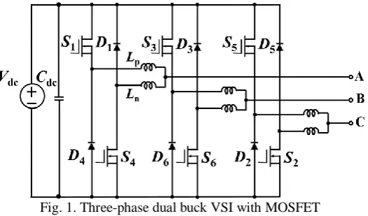
Fig. 1. Three-phase dual buck VSI with MOSFET
calculation, when implemented by a digital signal processor (DSP). The unified pulse width modulation is modified to use the current reference to generate the gate signals because of the unique operation principle of the three-phase dual-buck inverter. Different pulse width modulation methods are the special cases of the unified technique. It includes sinusoidal pulse width modulation (SPWM), space vector pulse width modulation (SVPWM), and discontinuous space vector pulse width modulation (DSVPWM). This paper presents the basic operation principle of the proposed dual buck inverter and it analyses the unified pulse width modulation technique applied to the three-phase dual-buck inverter and three level three phase cascade dual buck inverter`. It uses the closed-loop controller design with proportional-integral (PI) and proportional (P) controllers.
II. DUAL BUCK INVERTER
The three-phase dual-buck inverter has been shown in Fig. 1.The PWMs for the active switches are determined by the phase output current even though it is a voltage source inverter.
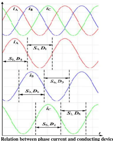
Fig. 2. Relation between phase current and conducting devices.
Fig. 2 shows the relation between the operation of switches and the polarity of phase current. For example take phase A, when iA is positive, S1 and D4 are the conducting devices and when iA is negative, S4 and D1 are the conducting devices. The operation principle is similar for phases B and C.
Shoot-through is no longer possible since there is only one active switch per leg. Therefore, the reliability of the three-phase dual-buck inverter is much higher when compared to traditional voltage source inverters. No dead time is needed because when S1 operates, S4 is always OFF and vice versa. Without the dead-time effect, the output waveforms are more sinusoidal and the energy is transferred more completely. Since the power MOSFET and diode can be selected independently, the system efficiency can be further improved.
III. UNIFIED PWM ANALYSIS
In many industrial applications, control of the output voltage of inverters is often necessary. The most efficient method of the controlling the gain and output voltage is to incorporate pulse width modulation control within the inverters.
discontinuous space vector pulse width modulation (DSVPWM). By using unified PWM methods, SVPWM and DSVPWM can be equivalently generated using triangle carrier comparison like SPWM. This will greatly reduces computational burden and is very easy to implement by digital signal processor.
Three-phase dual buck inverter is a hard switching VSI even though MOSFETs are used to cut down switching losses. Therefore, it is better to further reduce the switching loss by incorporating discontinuous space vector pulse width modulation.
Traditionally, the space vector PWM methods need to do trigonometric calculation and perform recombination of actual gating times, which is unfavorable for real-time implementation by a digital signal processor. Using unified pulse width modulation methods, space vector PWM and discontinuous space vector PWM can be equivalently generated using triangle carrier comparison like sinusoidal PWM which greatly reduces computational burden and is very easy to implement by DSP. Fig. 4 shows the unified PWM generation block diagram. Based on the current reference polarity, the switch to which PWM is applied is selected. shows the block diagram of unified pulse width modulation generation. The phase duty cycles da, db, and dc are provided by a closed-loop controller. The injected zero sequence duty cycle dzs is generated by the following equation
dzs= −[(1−2k0)+k0.dmax+(1−k0).dmin] (1)
Where dmax = max (da, db, dc) and dmin = min (da, db, dc). k0 is the pulse width modulation determination factor.
Under this unified PWM scheme when dzs=0, the output pulse width modulation will be sinusoidal pulse width modulation (SPWM). When k0 = 0.5, the output pulse width modulation is space vector pulse width modulation (SVPWM); when k0 follows the relation in (2), the output PWM is discontinuous space vector modulation (DSVPWM).
k0 = 1 , J >0
k0= 0 , J<0 (2) J = max (iaref, ibref, icref ) + min (iaref, ibref, icref).
IV. RESULTS
In normal operation, the dual buck inverter totally eliminates the shoot-through problems as discussed in section II. How ever, the gating signals for S1 and S4 might be high at the same time under some fault conditions. During this condition Lp and Ln are inserted in the shoot-through path through the dc power supply, and it will limit the di/dt of the devices, and thus the failure rate of the circuit is decreased and provide enough time for the protection circuit.
(a)
(b)
(c)
(a)
(b)
(c)
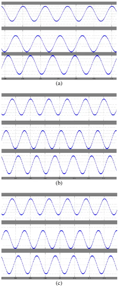
Fig.6. Three phase output voltage waveforms of 3 level inverter at dc bus voltage 380V. (a) SPWM. (b) SVPWM. (c) DSVPWM.
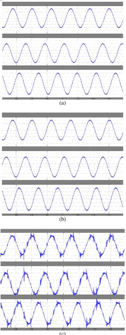
Fig. 5 shows three-phase output phase-to-neutral voltage waveforms of a three phase dual buck inverter for SPWM, SVPWM, and DSVPWM under dc bus voltage 380 V. The output voltage is 120 V.
Fig.6 shows three-phase output voltage waveforms of a three level cascaded dual buck inverter for SPWM, SVPWM, and DSVPWM under dc bus voltage 380V with duty cycle 0.9. Space vector PWM and discontinuous SVPWM can run at lower bus voltage, with the help of extended duty cycle, further reducing switching losses. By using a multilevel inverter the harmonics is further reduced.
V. CONCLUSION
REFERENCES
[1]. S-Y. Park, P.W.Sun, W.Yu and J-S. Lai, “Performance evaluation of high voltage super junction MOSFETs for zero-voltage soft switching inverter applications,” in Proc. 25th IEEE Appl. Power Electron. Conf.Expo.,Feb.2010,pp.387-392.
[2]. L. Saro, K. Dierberger and R.Redl,”High-Voltage MOSFET behavior in soft-switching converters: Analysis and reliability improvements,” in Proc. 20th IEEE Telecom. Energy Conf., 1998, pp.30-40. [3]. X.D. Huang, H.J. Yu, J-s Lai, A.R. Hefner, and D.W. Berning, “Characterization of paralleled super
junction MOSFET devices under hard and soft-switching conditions,” in Proc. 32nd IEEE Power Electron. Spec. Conf., 2001, vol.4, pp.2145-2150.
[4]. C.M. Johnson and V.Pickert, “Three-phase soft-switching voltage source converters for motor drives. II. Fundamental limitations and critical assessment,” IEE Proc. Electr. Power appl., vol.146, no.2, pp.155-162, Mar.1999.
[5]. V.Pickert and C.M. Johnson, “Three-phase soft-switching voltage source converters for motor drives.I. Overview and analysis,” IEE Proc. Electr. Power Appl.,vol. 146, no.2,pp.147-154,Mar. 1999.
[6]. P.W. Sun, J-S. Lai, H.Qian, W.S. Yu, C. Smith, and J.Bates, “High efficiency three-phase soft-switching inverter for electric vehicle drives,” in Proc. IEEE Vehicle Power Propulsion Conf.,Sep.2009,pp.761-766.
[7]. P.W. Sun, J-S.Lai, H.Qian, W.S. Yu, C. Smith, and J.Bates, B.Amet, A.Litvinov, and S.Leslie, “Efficiency evaluation of a 55kW soft-switching module based inverter for high temperature hybrid electric vehicle drives application,” in Proc. 25th IEEE Appl. Power Electron. Conf Expo., Feb. 2010,pp.474-479.
[8]. J. Liu and Y.Yan, “A novel hysteresis current controlled dual buck half bridge inverter,” in Proc. IEEE PESC, Jun.2003, pp.1615-1620.
[9]. Z.Yao, L.Xiao, and Y..Yan,”Dual-buck full-bridge inverter with hysteresis current control,” IEEE Trans.Ind.Electron., vol.56, no.8, pp.3153-3160, Aug.2009.
[10]. Z.Yao, L.Xiao, and Y.Yan,”Control strategy for series and parallel output dual-buck half bridge inverters based on DSP control,” IEEE Trans. Power Electron., vol.24, no.2, pp.434-444, Feb.2009. [11]. V.Blasko,”A hybrid PWM strategy combining modified space vector and triangle comparison
methods,” in Proc. 27th
IEEE Power Electron. Spec. Conf., Jun.1996, vol. 2, pp.1872-1878.
[12]. D.-W. Chung, J-S. Kim and S-K Sul,”Unified voltage modulation technique for real-time three-phase power conversion,” IEEE Trans. Ind. Appl., vol. 34, no.2, pp. 374-380, Mar./Apr.1998.