nRF24LU1+
Single Chip 2.4GHz Transceiver with USB
Microcontroller and Flash Memory
Product Specification v1.0
Key Features
• nRF24L01+ compatible RF transceiver • Worldwide 2.4GHz ISM band operation • Up to 2Mbps on air data rate
• Enhanced ShockBurst™ hardware link layer • Air compatible with nRF24LU1, nRF24LE1,
nRF24L01+, nRF24L01, nRF2401A, nRF2402, nRF24E1 and nRF24E2
• Low cost external ±60ppm 16MHz crystal • Full speed USB 2.0 compliant device controller • Up to 12 Mbps USB transfer rate
• 2 control, 10 bulk/interrupt and 2 ISO endpoints • Dedicated 512 bytes endpoint buffer RAM • Software controlled pull-up resistor for D+ • PLL for full-speed USB operation
• Voltage regulator, 4.0 to 5.25V supply range • Enhanced 8-bit 8051 compatible
microcontroller
• Drop-in compatibility with nRF24LU1 • Reduced instruction cycle time • 32-bit multiplication-division unit
• 16 or 32 kbytes of on-chip flash memory • 2 kbytes of on-chip SRAM
• 6 general purpose digital input/output pins • Hardware SPI slave and master, UART • 3 16-bit timers/counters
• AES encryption/decryption co-processor • Supports firmware upgrade over USB • Supports FS2 hardware debugger
Applications
• Compact USB dongles for wireless peripherals
• USB dongles for mouse, keyboards and remotes
• USB dongle 3-in-1 desktop bundles • USB dongle for advanced media center
remote controls
• USB dongle for game controllers • Toys
Liability disclaimer
Nordic Semiconductor ASA reserves the right to make changes without further notice to the product to improve reliability, function or design. Nordic Semiconductor ASA does not assume any liability arising out of the application or use of any product or circuits described herein.
All application information is advisory and does not form part of the specification.
Limiting values
Stress above one or more of the limiting values may cause permanent damage to the device. These are stress ratings only and operation of the device at these or at any other conditions above those given in the specifications are not implied. Exposure to limiting values for extended periods may affect device reliability.
Life support applications
These products are not designed for use in life support appliances, devices, or systems where malfunction of these products can reasonably be expected to result in personal injury. Nordic Semiconductor ASA cus-tomers using or selling these products for use in such applications do so at their own risk and agree to fully indemnify Nordic Semiconductor ASA for any damages resulting from such improper use or sale.
Contact details
For your nearest dealer, please see www.nordicsemi.no Main office: Otto Nielsens vei 12
7004 Trondheim Phone: +47 72 89 89 00
Fax: +47 72 89 89 89 www.nordicsemi.no Data sheet status
Objective product specification This product specification contains target specifications for product development.
Preliminary product specification This product specification contains preliminary data; supplementary data may be published from Nordic Semiconductor ASA later.
Product specification This product specification contains final product specifications. Nordic Semiconductor ASA reserves the right to make changes at any time without notice in order to improve design and supply the best possible product.
Revision History
Attention!
Date Version Description
January 2009 1.0
Observe precaution for handling Electrostatic Sensitive Device. HBM (Human Body Model): Class 1C CDM (Charged Device Model): Class IV
Contents
1 Introduction ... 12
1.1
Prerequisites ... 12
1.2
Writing conventions... 12
1.3
Features ... 13
1.4
Block diagram ... 14
1.5
Typical system usage... 15
2
Pin Information... 16
2.1
Pin Assignments ... 16
2.2
Pin Functions ... 17
2.2.1
Antenna pins... 17
2.2.2
USB pins... 17
2.2.3
Power supply pins ... 17
2.2.4
PROG pin ... 17
2.2.5
Reference current pin ... 18
2.2.6
Port pins ... 18
2.2.7
External RESET Pin ... 18
2.2.8
Crystal oscillator pins... 18
3
Absolute Maximum Ratings ... 19
4
Operating Conditions ... 20
5
Electrical Specifications... 21
5.1
Power consumption and timing characteristics ... 21
5.2
RF transceiver characteristics... 22
5.3
USB interface ... 25
5.4
Flash memory ... 25
5.5
Crystal specifications ... 26
5.6
DC Electrical Characteristics... 26
6
RF Transceiver ... 28
6.1
Features ... 28
6.2
Block diagram ... 29
6.3
Functional description ... 29
6.3.1
Operational Modes ... 29
6.3.1.1
State diagram ... 29
6.3.1.2
Power down mode... 30
6.3.1.3
Standby modes ... 30
6.3.1.4
RX mode ... 31
6.3.1.5
TX mode... 31
6.3.1.6
Operational modes configuration ... 32
6.3.1.7
Timing information... 32
6.3.2
Air data rate ... 33
6.3.3
RF channel frequency ... 33
6.3.4
Received Power Detector measurements ... 33
6.3.5
PA control ... 33
6.3.6
RX/TX control ... 34
6.4.1
Features ... 34
6.4.2
Enhanced ShockBurst™ overview ... 34
6.4.3
Enhanced Shockburst™ packet format ... 35
6.4.3.1
Preamble ... 35
6.4.3.2
Address ... 35
6.4.3.3
Packet Control Field ... 36
6.4.3.4
Payload ... 36
6.4.3.5
CRC (Cyclic Redundancy Check) ... 37
6.4.4
Automatic packet assembly... 38
6.4.5
Automatic packet disassembly ... 39
6.4.6
Automatic packet transaction handling... 40
6.4.6.1
Auto Acknowledgement... 40
6.4.6.2
Auto Retransmission (ART)... 40
6.4.7
Enhanced ShockBurst flowcharts... 42
6.4.7.1
PTX operation ... 42
6.4.7.2
PRX operation ... 44
6.4.8
MultiCeiver™ ... 45
6.4.9
Enhanced ShockBurst™ timing... 47
6.4.10
Enhanced ShockBurst™ transaction diagram... 50
6.4.10.1
Single transaction with ACK packet and interrupts ... 51
6.4.10.2
Single transaction with a lost packet ... 51
6.4.10.3
Single transaction with a lost ACK packet... 52
6.4.10.4
Single transaction with ACK payload packet... 52
6.4.10.5
Single transaction with ACK payload packet and lost packet... 53
6.4.10.6
Two transactions with ACK payload packet and the first
ACK packet lost ... 53
6.4.10.7
Two transactions where max retransmissions is reached... 54
6.4.11
Compatibility with ShockBurst™... 54
6.4.11.1
ShockBurst™ packet format... 54
6.5
Data and control interface ... 55
6.5.1
SFR registers... 55
6.5.2
SPI operation... 56
6.5.2.1
SPI commands ... 56
6.5.3
Data FIFO... 57
6.5.4
Interrupt ... 58
6.6
Register map... 59
6.6.1
Register map table ... 59
7
USB Interface... 65
7.1
Features ... 65
7.2
Block diagram ... 66
7.3
Functional description ... 67
7.4
Control endpoints ... 71
7.4.1
Control endpoint 0 implementation... 71
7.4.2
Endpoint 0 registers ... 72
7.4.3.2
Control read transfer example ... 74
7.4.3.3
No-data control transfer example ... 74
7.5
Bulk/Interrupt endpoints ... 75
7.5.1
Bulk/Interrupt endpoints implementation ... 75
7.5.2
Bulk/Interrupt endpoints registers ... 75
7.5.3
Bulk and interrupt endpoints initialization ... 76
7.5.3.1
Bulk and interrupt transfers ... 76
7.5.4
Data packet synchronization ... 77
7.5.5
Endpoint pairing... 78
7.5.5.1
Paired IN endpoint status ... 78
7.5.5.2
Paired OUT endpoint status ... 78
7.6
Isochronous endpoints ... 78
7.6.1
Isochronous endpoints implementation ... 78
7.6.2
Isochronous endpoints registers ... 79
7.6.3
ISO endpoints initialization ... 79
7.6.4
ISO transfers ... 79
7.6.4.1
ISO IN transfers ... 79
7.6.4.2
ISO OUT transfers ... 80
7.7
Memory configuration... 80
7.7.1
On-chip memory map ... 80
7.7.2
Setting ISO FIFO size... 81
7.7.3
Setting Bulk OUT size ... 82
7.7.4
Setting Bulk IN size ... 82
7.8
The USB controller interrupts... 83
7.8.1
Wakeup interrupt request ... 83
7.8.2
USB interrupt request ... 83
7.8.3
USB interrupt vectors ... 86
7.9
The USB controller registers ... 86
7.9.1
Bulk IN data buffers (inxbuf) ... 86
7.9.2
Bulk OUT data buffers (outxbuf)... 87
7.9.3
Isochronous OUT endpoint data FIFO (out8dat) ... 87
7.9.4
Isochronous IN endpoint data FIFOs (in8dat) ... 87
7.9.5
Isochronous data bytes counter (out8bch/out8bcl) ... 87
7.9.6
Isochronous transfer error register (isoerr) ... 87
7.9.7
The zero byte count for ISO OUT endpoints (zbcout) ... 88
7.9.8
Endpoints 0 to 5 IN interrupt request register (in_irq) ... 88
7.9.9
Endpoints 0 to 5 OUT interrupt request register (out_irq) ... 88
7.9.10
The USB interrupt request register (usbirq) ... 88
7.9.11
Endpoint 0 to 5 IN interrupt enables (In_ien) ... 89
7.9.12
Endpoint 0 to 5 OUT interrupt enables (out_ien) ... 89
7.9.13
USB interrupt enable (usbien) ... 89
7.9.14
Endpoint 0 control and status register (ep0cs) ... 90
7.9.15
Endpoint 0 to 5 IN byte count registers (inxbc) ... 91
7.9.16
Endpoint 1 to 5 IN control and status registers (inxcs) ... 91
7.9.17
Endpoint 0 to 5 OUT byte count registers (outxbc) ... 92
7.9.19
USB control and status register (usbcs) ... 93
7.9.20
Data toggle control register (togctl) ... 93
7.9.21
USB frame count low (usbframel/usbframeh) ... 94
7.9.22
Function address register (fnaddr) ... 94
7.9.23
USB endpoint pairing register (usbpair) ... 94
7.9.24
Endpoints 0 to 5 IN valid bits (Inbulkval) ... 94
7.9.25
Endpoints 0 to 5 OUT valid bits (outbulkval) ... 95
7.9.26
Isochronous IN endpoint valid bits (inisoval) ... 95
7.9.27
Isochronous OUT endpoint valid bits (outisoval) ... 95
7.9.28
SETUP data buffer (setupbuf) ... 95
7.9.29
ISO OUT endpoint start address (out8addr) ... 95
7.9.30
ISO IN endpoint start address (in8addr) ... 95
8
Encryption/Decryption Unit... 96
8.1
Features ... 96
8.1.1
ECB – Electronic Code Book... 96
8.1.2
CBC – Cipher Block Chaining ... 96
8.1.3
CFB – Cipher FeedBack... 97
8.1.4
OFB – Output FeedBack mode ... 97
8.1.5
CTR – Counter mode ... 97
8.2
Functional description ... 98
9
SPI master ... 101
9.1
Block diagram ... 101
9.2
Functional description ... 101
9.3
SPI operation ... 102
10
SPI slave ... 103
10.1
Block diagram ... 103
10.2
Functional description ... 103
10.3
SPI timing ... 104
11
Timer/Counters ... 105
11.1
Features ... 105
11.2
Block diagram ... 105
11.3
Functional description ... 105
11.3.1
Timer 0 and Timer 1 ... 105
11.3.1.1
Mode 0 and Mode 1 ... 106
11.3.1.2
Mode 2 ... 107
11.3.1.3
Mode 3 ... 108
11.3.2
Timer 2 ... 108
11.3.2.1
Timer 2 description ... 109
11.3.2.2
Timer mode ... 109
11.3.2.3
Event counter mode ... 109
11.3.2.4
Gated timer mode ... 109
11.3.2.5
Timer 2 reload ... 110
11.4
SFR registers ... 110
11.4.1
Timer/Counter control register – TCON ... 110
11.4.4
Timer1 – TH1, TL1 ... 111
11.4.5
Timer 2 control register – T2CON ... 112
11.4.6
Timer 2 – TH2, TL2 ... 112
11.4.7
Compare/Capture enable register – CCEN ... 113
11.4.8
Capture registers – CC1, CC2, CC3 ... 113
11.4.9
Compare/Reload/Capture register – CRCH, CRCL ... 114
12
Serial Port (UART) ... 115
12.1
Features ... 115
12.2
Block diagram ... 115
12.3
Functional description ... 115
12.4
SFR registers ... 116
12.4.1
Serial Port 0 control register – S0CON ... 116
12.4.2
Serial port 0 data buffer – S0BUF ... 117
12.4.3
Serial port 0 reload register – S0RELH, S0RELL ... 117
12.4.4
Serial Port 0 baud rate select register - WDCON ... 117
13
Input/Output port (GPIO) ... 118
13.1
Normal IO ... 118
13.2
Expanded IO ... 120
14
MCU ... 121
14.1
Features ... 121
14.2
Block diagram ... 122
14.3
Arithmetic Logic Unit (ALU) ... 123
14.4
Instruction set summary ... 123
14.5
Opcode map ... 127
15
Memory and I/O organization ... 129
15.1
Special function registers ... 130
15.1.1
Special function registers locations ... 130
15.1.2
Special function registers reset values ... 131
15.1.3
Accumulator - ACC ... 133
15.1.4
B register – B ... 133
15.1.5
Program Status Word register - PSW ... 134
15.1.6
Stack Pointer – SP ... 134
15.1.7
Data Pointer – DPH, DPL ... 134
15.1.8
Data Pointer 1 – DPH1, DPL1 ... 135
15.1.9
Data Pointer Select register – DPS ... 135
16
Random Access Memory (RAM) ... 136
16.1
Cycle control ... 136
17
Flash Memory ... 137
17.1
Features ... 137
17.2
Block diagram ... 137
17.3
Functional description ... 137
17.3.1
Flash memory configuration ... 137
17.3.2
InfoPage content ... 139
17.3.3
Protected pages and data pages ... 139
17.3.4
16 kB Flash memory size option ... 140
17.3.6
SFR registers for flash memory operations ... 141
17.4
Brown-out ... 141
17.5
Flash programming from the MCU ... 142
17.5.1
MCU write and erase of the MainBlock ... 142
17.5.2
Hardware support for firmware upgrade ... 143
17.6
Flash programming through USB ... 143
17.6.1
Flash Layout ... 143
17.6.2
USB Protocol ... 144
17.6.2.1
Firmware Version (cmd id 0x01) ... 145
17.6.2.2
Flash Write Init (cmd 0x02) ... 145
17.6.2.3
Read Flash (cmd 0x03) ... 145
17.6.2.4
Flash Page Erase (cmd 0x04) ... 146
17.6.2.5
Turn on flash MainBlock readback disable (cmd 0x05) ... 146
17.6.2.6
Select flash half (cmd 0x06) ... 146
17.7
Flash programming through SPI ... 147
17.7.1
SPI commands ... 147
17.7.1.1
WREN/WRDIS ... 149
17.7.1.2
RDSR ... 149
17.7.1.3
WRSR ... 149
17.7.1.4
READ ... 149
17.7.1.5
PROGRAM ... 149
17.7.1.6
ERASE PAGE ... 150
17.7.1.7
ERASE ALL ... 150
17.7.1.8
RDFPCR ... 150
17.7.1.9
RDISIP ... 151
17.7.1.10
RDISMB ... 151
17.7.1.11
ENDEBUG ... 151
17.7.1.12
SPI Readback disable ... 152
17.7.2
Standalone programming requirements ... 152
17.7.2.1
Clock requirements ... 153
17.7.2.2
Power supply requirements ... 154
17.7.2.3
Signal pin requirements ... 154
17.7.3
In circuit programming over SPI ... 155
17.7.4
SPI programming sequences ... 155
17.7.4.1
Erasing and programming the InfoPage ... 156
18
MDU – Multiply Divide Unit ... 158
18.1
Features ... 158
18.2
Block diagram ... 158
18.3
Functional description ... 158
18.4
SFR registers ... 158
18.4.1
a) Loading the MDx registers ... 159
18.4.2
b) Executing calculation ... 160
18.4.3
c) Reading the result from the MDx registers ... 160
18.4.4
d) Normalizing ... 160
18.4.7
g) The mdov flag ... 161
19
Watchdog and wakeup functions ... 162
19.1
Features ... 162
19.2
Block diagram ... 162
19.3
Functional description ... 163
19.3.1
The Low Frequency Clock (CKLF) ... 163
19.3.2
Tick calibration ... 163
19.3.3
RTC wakeup timer ... 163
19.3.4
Programmable GPIO wakeup function ... 164
19.3.5
Watchdog ... 164
19.3.6
Programming interface to watchdog and wakeup functions ... 164
20
Power management ... 167
20.1
Features ... 167
20.2
Block diagram ... 167
20.3
Modes of operation ... 168
20.4
Functional description ... 169
20.4.1
Clock control – CLKCTL ... 169
20.4.2
Power down control – PWRDWN ... 170
20.4.3
Reset result – RSTRES ... 170
20.4.4
Wakeup configuration register – WUCONF ... 170
20.4.5
Power control register - PCON ... 171
21
Power supply supervisor ... 172
21.1
Features ... 172
21.2
Functional description ... 172
21.2.1
Power-on reset ... 172
21.2.2
Brown-out detection ... 172
22
Interrupts ... 173
22.1
Features ... 173
22.2
Block diagram ... 173
22.3
Functional description ... 174
22.4
SFR registers ... 174
22.4.1
Interrupt enable 0 register – IEN0 ... 174
22.4.2
Interrupt enable 1 register – IEN1 ... 175
22.4.3
Interrupt priority registers – IP0, IP1 ... 175
22.4.4
Interrupt request control registers – IRCON ... 176
23
HW debugger support ... 177
23.1
Features ... 177
23.2
Functional description ... 177
24
Peripheral information ... 178
24.1
Antenna output ... 178
24.2
Crystal oscillator ... 178
24.3
PCB layout and decoupling guidelines ... 178
25
Application example ... 180
25.1
Schematics ... 180
25.2
Layout ... 180
26
Mechanical specifications ... 182
27
Ordering information ... 183
27.1
Package marking ... 183
27.1.1
Abbreviations ... 183
27.2
Product options ... 184
27.2.1
RF silicon ... 184
27.2.2
Development tools ... 184
28
Glossary of terms ... 185
Appendix A - (USB memory configurations) ... 186
Configuration 1 ... 186
Configuration 2 ... 186
Configuration 3 ... 187
Configuration 4 ... 188
1 Introduction
The nRF24LU1+ is a unique single chip solution for compact USB dongles. The internal nRF24L01+ 2.4GHz RF transceiver supports a wide range of applications including PC peripherals, sports accessories and game peripherals.
With an air data rate of 2 Mbps combined with full speed USB, supporting up to 12 Mbps, the nRF24LU1+ meets the stringent performance requirements of applications such as wireless mouse, game controllers and media center remote controls with displays.
The nRF24LU1+ integrates:
• A nRF24L01+ 2.4GHz RF transceiver
• A full speed USB 2.0 compliant device controller • An 8-bit microcontroller
• 16 or 32 kbytes of flash memory
All this is packaged on a compact 5x5mm package, low cost external BOM.
With an internal voltage regulator that enables the chip to be powered directly from the USB bus, it does not require an external voltage regulator, saving cost and board space. With a fully integrated RF synthe-sizer and PLL for the USB no external loop filters, resonators or VCO varactor diodes are required. All that is needed is a low cost ±60ppm 16MHz crystal, matching circuitry and the antenna.
The main benefits of nRF24LU1+ are: • Very compact USB dongle • Low cost external BOM
• No need for an external voltage regulator • Single low cost ±60ppm 16MHz crystal • Flash memory for firmware upgrades
1.1 Prerequisites
In order to fully understand the product specification, a good knowledge of electronic and software engi-neering is necessary.
1.2 Writing conventions
This product specification follows a set of typographic rules that makes the document consistent and easy to read. The following writing conventions are used:
• Commands, bit state conditions, and register names are written in Courier.
• Pin names and pin signal conditions are written in Courier bold.
1.3 Features
Features of the nRF24LU1+ include: • Fast 8-bit MCU:
X Intel MCS 51 compliant instruction set
X Reduced instruction cycle time, up to 12x compared to legacy 8051 X 32 bit multiplication – division unit
• Memory:
X 16 or 32 kbytes of on-chip flash memory with security features X 2 kbytes of on-chip RAM memory
X Pre-programmed USB bootloader in the on-chip flash memory. • 6 programmable digital input/output pins configurable as:
X GPIO X SPI master X SPI slave
X External interrupts X Timer inputs
X Full duplex serial port X Debug interface
• High performance 2.4 GHz RF-transceiver X True single chip GFSK transceiver X Complete OSI Link Layer in hardware
X Enhanced ShockBurst™ link layer support in HW: X Packet assembly/disassembly
X Address and CRC computation X Auto ACK and retransmit
X On the air data rate 250 kbps, 1 Mbps or 2 Mbps X Digital interface (SPI) speed 0-8 Mbps
X 125 RF channel operation, 79 (2.402-2.81 GHz) channels within 2.400 - 2.4853 GHz. X Short switching time enable frequency hopping
X Fully RF compatible with nRF24LXX
X RF compatible with nRF2401A, nRF2402, nRF24E1, nRF24E2 in 250 kbps and 1 Mbps mode • AES encryption/decryption HW-block with 128 bits key length
X ECB – Electronic Code Book mode X CBC – Cipher Block Chaining X CFB – Cipher FeedBack mode X OFB – Output FeedBack mode X CTR – Counter mode
• Full speed USB 2.0 compliant device controller supporting: X Data transfer rates up to 12 Mbit/s
X Control, Interrupt, Bulk and ISO data transfer X Endpoint 0 for control
X 5 input and 5 output Bulk/Interrupt endpoints X 1 input and 1 output iso-synchronous endpoints
X Total 512 bytes of USB buffer endpoint memory sharable between endpoints X On-chip USB transceiver PHY
X On-chip pull-up resistor on D+ line with software controlled disconnect • Power management function:
X Low power design supporting fully static stop/ standby/ suspend modes X Programmable MCU clock frequency from 64 kHz to 16 MHz
• On-chip oscillator and PLL to obtain full speed USB operation and to reduce the need for external components
• On-chip power on reset generator and brown-out detector
• On-chip support for FS2 and nRFprobeTM HW debugger, supported by Keil development tools. • Complete firmware platform available:
X Hardware abstraction layer (HAL) Functions X USB library Functions
X Standard and HID specific USB Requests and Descriptors X nRF24LU1+ Library functions
X AES HAL
X Application examples X Device Firmware Upgrade
1.4 Block diagram
Figure 1. nRF24LU1+ block diagram
To find more information on the block diagram, see Table 1. below:
Name Reference
USB chapter 7 on page 65
FLASH chapter 17 on page 137
SRAM chapter 15 on page 129
2.4GHz RF transceiver chapter 6 on page 28
XOSC section 24.2 on page 178
Enhanced ShockBurstTM section 6.4 on page 34
IRAM chapter 16 on page 136
MCU chapter 14 on page 121
RTC, Watchdog and Wakeup chapter 19 on page 162
SPI Master chapter 9 on page 101
Interrupt control chapter 21 on page 172
MEM-bus SFR-bus USB FLASH 16/32 kbytes SRAM 2 kbytes PLL 48MHz XOSC 16MHz
RTC Watchdog Wakeup
Slow clock bridge
2.4GHz RF Transceiver Enhanced ShockBurst SPI Master MCU 8051 AES co-processor Power Management Brown-out Detector IRAM 256 byte Interrupt Control Voltage regulator Power on reset
OCI SPI Master/Slave
Table 1. Block diagram cross references
1.5 Typical system usage
Figure 2. Typical system usage
SPI master/slave chapter 9 on page 101 and chapter 10 on page 103 AES co-processor chapter 8 on page 96
Power management chapter 20 on page 167 Brown-out detector section 17.4 on page 141
Name Reference Antenna Matching Xtal nRF24LU1+ ESD USB C onnector
2 Pin Information
2.1 Pin Assignments
Figure 3. nRF24LU1+ pin assignment (top view) for a QFN32 5x5 mm package.
VDD
VBUS
VDD
D+
D-VSS
PROG
RESET
VDD
VSS
ANT2
ANT1
VDD_PA
VDD
VSS
VSS
VDD
P
0.0
P
0.1
VSS
P
0.2
P
0.3
P
0.4
P
0.5
VSS
XC1
XC2
DEC
2
DEC
1
VDD
VSS
IRE
F
1 2 3 4 5 6 7 8 24 23 22 21 20 19 18 17 9 10 11 12 13 14 15 16 25 26 27 28 29 30 31 32nRF24LU1+
QFN32 5X5
2.2 Pin Functions
Table 2. nRF24LU1+ pin functions
2.2.1 Antenna pins
ANT1 and ANT2 are connections for the external antenna (both receive and transmit).
2.2.2 USB pins
D- and D+ are the connections to the USB data lines. External ESD protection is recommended.
2.2.3 Power supply pins
VBUS and VSS are the power supply and ground pins. The nRF24LU1+ can operate from a single power
supply.
The nRF24LU1+ contains an on-chip regulator that produces +3.3V on the VDD pins, from the VBUS supply
line (4.0 – 5.25 V). Alternatively, the VBUS pin can be left open and the VDD pins may be fed from an
exter-nal 3.3V supply. In this case, the on-chip 3.3V regulator is switched off.
Additional on-chip regulators produce voltages for internal analog and digital functions blocks. External decoupling capacitors are required on DEC1 and DEC2.
VDD_PA is a 1.8V output that is used to switch on an external RF Power Amplifier.
2.2.4 PROG pin
When set high this pin enables external flash programming and Port 0 is configured as a slave SPI port. The PROG pin needs an external pull-down resistor.
Pin Name Type Description
21, 22 ANT1, ANT2 RF Antenna connection
5, 4 D-, D+ Digital I/O USB data
28, 29 DEC1, DEC2 Power Positive Digital Supply output for de-coupling
pur-poses
25 IREF Analog Input Reference current
10, 11, 13, 14, 15, 16
P0.0 – P0.5 Digital I/O General purpose data Port 0, bit 0 - 5. See Table 99.
on page 120 for alternative pin functions. 7 PROG Digital Input Reserved for programming the flash
8 RESET Digital Input Reset for MCU, active low
2 VBUS Power USB power connection
1, 3, 9, 19, 24, 27
VDD Power Alternative power supply pins. The VDD pins must
always be connected and de-coupled externally.
20 VDD_PA Power Output Power Supply (+1.8V) to Power Amplifier
6, 12, 17, 18, 23, 26, 30
VSS Power Ground (0V)
32, 31 XC1, XC2 Analog Input Crystal connection
Exposed die pad
Power/heat relief
2.2.5 Reference current pin
IREF pin must be connected to an external resistor.
2.2.6 Port pins
P0.0 – P0.5 are six general purpose I/O pins. Their functions are described in chapter 13 on page 118.
2.2.7 External RESET Pin
A logic 0 on the RESET pin forces the nRF24LU1+ to a known start-up state.
2.2.8 Crystal oscillator pins
3 Absolute Maximum Ratings
Maximum ratings are the extreme limits that you can expose the nRF24LU1+ to without permanently dam-aging it. Exposure to absolute maximum ratings for prolonged periods of time may affect device reliability.
Table 3. Absolute maximum ratings
Operating conditions Minimum Maximum Units Supply voltages VBUS -0.3 +5.75 V VSS 0 V VDD -0.3 +3.6 V Input voltage VI -0.3 +3.6 V
Total Power Dissipation
PD (TA=85°C) 180 mW
Temperatures
Operating Temperature -40 +85 °C
4 Operating Conditions
Table 4. Operating conditions
Symbol Parameter (condition) Notes Min. Typ. Max. Units
VBUS Supply voltage 4.0 5 5.25 V
VDD Alternative supply voltage 3.05 3.27 3.5 V
5 Electrical Specifications
This section contains electrical and timing specifications.
5.1 Power consumption and timing characteristics
Table 5. Power consumption and timing characteristics
Symbol Parameter (condition) Notes Min. Typ. Max. Units IOP Average supply current in operating
mode
a
a. MCU running radio receive at 2Mbps and USB transmit
24 mA
ISTANDBY Supply current in standby mode b
b. When MCU is in standby, USB is suspended and the RF Transceiver is in standby
480 µA
MCU
IMCU16MPLL Running @ 16MHz, generated from PLL 6.3 mA
IMCU12MPLL Running @ 12MHz, generated from PLL 5 mA
IMCU8MPLL Running @ 8MHz, generated from PLL 4 mA
IMCU4MPLL Running @ 4MHz, generated from PLL 3 mA
IMCU1.6MPLL Running @ 1.6MHz, generated from PLL
2 mA
IMCU4MXO Running @ 4MHz, generated from XO 2.4 mA
IMCU1.6MXO Running @ 1.6MHz, generated from XO 1.75 mA
IMCU.32MXO Running @ 0.32MHz, generated from XO
1.1 mA
IMCU64KXO Running @ 0.064MHz, generated from XO
1 mA
Trst_act From RESET to MCU active 2 ms
Tint_act From INTERRUPT to MCU active 300 µs
Tact_stby MCU from active to standby c
c. Measured from start of the software instruction which executes the change of mode, see also Table 15.
32 µs
RF Transceiver
ITX RF Transceiver TX current @0dBm out-put power
11.1 mA
RF Transceiver RX current @ 2Mbps 13.3 mA
IRX RF Transceiver RX current @ 1Mbps 12.9 mA
Tstby2a RF Transceiver from standby to active c 130 µs
Trst_radio From RESET to RF Transceiver power down
50 ms
USB
IUSB USB active current 4.4 mA
Tusb_wh USB wakeup from host 500 µs
Tusb_wmcu USB wakeup from MCU 300 µs
Tusbact_susp USB from active to suspend c 32 µs
PLL
Tplloff_on PLL from off to on time cd
d. Only possible when USB is in suspend mode
250 µs
5.2 RF transceiver characteristics
Symbol Parameter (condition) Notes Min. Typ. Max. Units General RF conditions
fOP Operating frequency a 2400 2525 MHz
PLLres PLL Programming resolution 1 MHz
fXTAL Crystal frequency 16 MHz
Δf250 Frequency deviation @ 250kbps ±160 kHz
Δf1M Frequency deviation @ 1Mbps ±160 kHz
Δf2M Frequency deviation @ 2Mbps ±320 kHz
RGFSK Air data rate b 250 2000 kbps
FCHANNEL 1MNon-overlapping channel spacing @ 250kbps/1 Mbps)
c 1 MHz
FCHANNEL 2MNon-overlapping channel spacing @ 2 Mbps
2 MHz
Transmitter operation
PRF Maximum output power d 0 +4 dBm
PRFC RF power control range 16 18 20 dB
PRFCR RF power accuracy ±4 dB
PBW2 20dB bandwidth for modulated carrier (2 Mbps)
1800 2000 kHz
PBW1 20dB bandwidth for modulated carrier (1 Mbps)
950 1100 kHz
PBW250 20dB bandwidth for modulated carrier (250 kbps)
700 800 kHz
PRF1.2 1st Adjacent Channel Transmit Power 2MHz (2Mbps)
-20 dBc
PRF2.2 2nd Adjacent Channel Transmit Power 4MHz (2Mbps)
-45 dBc
PRF1.1 1st Adjacent Channel Transmit Power 1MHz (1Mbps)
-20 dBc
PRF2.1 2nd Adjacent Channel Transmit Power 2MHz (1Mbps)
-40 dBc
PRF1.250 1st Adjacent Channel Transmit Power 1MHz (250kbps)
-25 dBc
PRF2.250 2nd Adjacent Channel Transmit Power 2MHz (250kbps)
-40 dBc
Receiver operation
RXMAX Maximum received signal at < 0.1% BER
0 dBm
RXSENS Sensitivity (0.1% BER) @ 2 Mbps -82 dBm
RXSENS Sensitivity (0.1% BER) @ 1 Mbps -85 dBm
RXSENS Sensitivity (0.1% BER) @ 250 kbps e -94 dBm
RX selectivity according to ETSI EN 300 440-1 V1.3.1 (2001-09) page 27
C/ICO C/I co-channel (2 Mbps) 7 dBc
C/I1ST 1st ACS (Adjacent Channel Selectivity), C/I 2MHz (2 Mbps)
3 dBc
C/I3RD 3rd ACS, C/I 6MHz (2 Mbps) -21 dBc C/INth Nth ACS, C/I f
i > 12MHz (2 Mbps) f -40 dBc
C/INth Nth ACS, C/I f
i > 36MHz (2 Mbps) -48 dBc
C/ICO C/I co-channel (1 Mbps) 9 dBc
C/I1ST 1st ACS, C/I 1MHz (1 Mbps) 8 dBc
C/I2ND 2nd ACS, C/I 2MHz (1 Mbps) -20 dBc
C/I3RD 3rd ACS, C/I 3MHz (1 Mbps) -30 dBc
C/INth Nth ACS, C/I fi > 6MHz (1 Mbps) -40 dBc
C/INth Nth ACS, C/I f
i > 25MHz (1 Mbps) f -47 dBc
C/ICO C/I co-channel (250 kbps) 12 dBc
C/I1ST 1st ACS, C/I 1MHz (250 kbps) -12 dBc
C/I2ND 2nd ACS, C/I 2MHz (250 kbps) -33 dBc
C/I3RD 3rd ACS, C/I 3MHz (250 kbps) -38 dBc
C/INth Nth ACS, C/I fi > 6MHz (250 kbps) -50 dBc
C/INth Nth ACS, C/I fi > 25MHz (250 kbps) f -60 dBc
RX selectivity with nRF24L01 equal modulation on interfering signal (Pin = -67dBm for wanted signal)
C/ICO C/I co-channel (2 Mbps) (modulated carrier)
11 dBc
C/I1ST 1st ACS (Adjacent Channel Selectivity), C/I 2MHz (2 Mbps)
4 dBc
C/I2ND 2nd ACS, C/I 4MHz (2 Mbps) -18 dBc
C/I3RD 3rd ACS, C/I 6MHz (2 Mbps) -24 dBc
C/INth Nth ACS, C/I fi > 12MHz (2 Mbps) -40 dBc
C/INth Nth ACS, C/I f
i > 36MHz (2 Mbps) -48 dBc
C/ICO C/I co-channel (1 Mbps) 12 dBc
C/I1ST 1st ACS, C/I 1MHz (1 Mbps) 8 dBc
C/I2ND 2nd ACS, C/I 2MHz (1 Mbps) -21 dBc
C/I3RD 3rd ACS, C/I 3MHz (1 Mbps) -30 dBc
C/INth Nth ACS, C/I fi > 6MHz (1 Mbps) -40 dBc
C/INth Nth ACS, C/I fi > 25MHz (1 Mbps) -50 dBc
C/ICO C/I co-channel (250 kbps) 7 dBc
C/I1ST 1st ACS, C/I 1MHz (250 kbps) -12 dBc
C/I2ND 2nd ACS, C/I 2MHz (250 kbps) -34 dBc
C/I3RD 3rd ACS, C/I 3MHz (250 kbps) -39 dBc
C/INth Nth ACS, C/I f
i > 6MHz (250 kbps) -50 dBc
C/INth Nth ACS, C/I fi > 25MHz (250 kbps) -60 dBc
RX intermodulation performance according to Bluetooth specification version 2.0, 4th November 2004, page 42
P_IM(6) @ 2Mbps
Input power of IM interferers at 6 and 12MHz distance from wanted signal
g -42 dBm
P_IM(8) Input power of IM interferers at 8 and g -38 dBm
Table 6. RF Transceiver specifications
P_IM(10) @ 2Mbps
Input power of IM interferers at 10 and 20MHz distance from wanted signal
g -37 dBm
P_IM(3) @ 1Mbps
Input power of IM interferers at 3 and 6MHz distance from wanted signal
g -36 dBm
P_IM(4) @ 1Mbps
Input power of IM interferers at 4 and 8MHz distance from wanted signal
g -36 dBm
P_IM(5) @ 1Mbps
Input power of IM interferers at 5 and 10MHz distance from wanted signal
g -36 dBm
P_IM(3) @ 250kbps
Input power of IM interferers at 3 and 6MHz distance from wanted signal
g -36 dBm
P_IM(4) @ 250kbps
Input power of IM interferers at 4 and 8MHz distance from wanted signal
g -36 dBm
P_IM(5) @ 250kbps
Input power of IM interferers at 5 and 10MHz distance from wanted signal
g -36 dBm
a. Usable band is determined by local regulations. b. Data rate in each burst on-air.
c. The minimum channel spacing is 1MHz. d. Antenna load impedance = 15Ω + j88Ω.
e. For 250 kpbs sensitivity, frequencies which are integer multiples of 16MHz (2400, 2416 and so on) sensi-tivity are reduced.
f. Narrow Band (In Band) Blocking measurements:
0 to ±40MHz; 1MHz step size
For Interferer frequency offsets n*2*fxtal, blocking performance is degraded by approximately 5dB com-pared to adjacent figures.
g. Wanted signal level at Pin = -64dBm. Two interferers with equal input power are used. The interferer clos-est in frequency is unmodulated, the other interferer is modulated equal with the wanted signal. The input power of interferers where the sensitivity equals BER = 0.1% is presented.
5.3 USB interface
The USB interface electrical performance is compliant with the USB specification 2.0.
Table 7. USB interface characteristics
5.4 Flash memory
Table 8. Flash memory characteristics
Table 9. Flash memory and page size
Characteristic Symbol Conditions Min. Typ. Max Unit Electrical characteristics
Input high voltage (driven) VIH 2.0 V
Input low voltage VIL 0.8 V
Differential input sensitivity VDI |(D+) – (D-)| 0.2 V
Differential common mode range VCM Includes VDI range
0.8 2.5 V
Single ended receiver threshold VSE 0.8 2.0 V
Single ended receiver hysteresis VSEH 200 mV
Output low voltage VOL 0 0.3 V
Output high voltage VOH 2.8 3.6 V
Differential output signal cross-point voltage
VCRS 1.3 2.0 V
Internal pull-up resistor (Standby mode)
RPU1 900 1100 1575 Ω
Internal pull-up resistor (Active mode) RPU2 1425 2100 3090 Ω
Termination voltage connected to RPU VTRM 3.05 3.5 V
Output driver resistance (does not include the series resistance)
ZDRV Steady state drive
15 Ω
Timing characteristics
Driver rise time TFR CL=50pF 4 20 ns
Driver fall time TFF CL=50pF 4 20 ns
Rise/fall time matching TFRFF TRF / TFF 90 111 %
Transceiver pad capacitance CIN Pad to ground 20 pF
Characteristic Symbol Conditions Min. Typ. Max Unit
Endurance Nendur 1000 cycles
Data retention Tret 25°C 100 years
Name Size Unit
Flash memory MainBlock 32768 bytes
Flash InfoPage 512 bytes
5.5 Crystal specifications
Table 10. Crystal specifications
5.6 DC Electrical Characteristics
Table 11. DC characteristics
Table 12. Digital input pin
Symbol Parameter (condition) Notes Min. Typ. Max. Units
fNOM Nominal frequency (parallel resonant) 16.000 MHz
fTOL Frequency tolerance ab
a. Includes initial accuracy, stability over temperature, aging and frequency pulling due to incorrect load capacitance.
b. Frequency regulations in certain regions set tighter requirements on frequency tolerance (e.g. Japan and South Korea max ±50ppm).
±60 ppm
CL Load capacitance 12 16 pF
C0 Shunt capacitance 3 7 pF
ESR Equivalent series resistance 50 100 Ω
PD Drive level 100 µW
Symbol Parameter (condition) Notes Min. Typ. Max. Units Operating conditions
VBUS Supply voltage 4.0 5.0 5.25 V
TEMP Operating Temperature -40 +27 +85 ºC
On-chip voltage regulators
VDD Output voltage a
a. Also valid for VDD input voltage.
3.05 3.27 3.5 V
IVDD External load current 2 mA
Symbol Parameter (condition) Notes Min. Typ. Max. Units
VIH HIGH level input voltage 0.7 VDD VDD V
Table 13. Digital output pin
Symbol Parameter (condition) Notes Min. Typ. Max. Units VOH HIGH level output voltage
(IOH= -1.0mA)
a VDD-0.3 VDD V
VOL LOW level output voltage (IOL= 1.0mA))
VSS 0.3 V
a. When the nRF24LU1+ is supplied from VBUS, there is a limit (IVDD) on the current that can be drawn from VDD by external devices. Current sourced by high outputs are supplied to external devices for this purpose.
6 RF Transceiver
The nRF24LU1+ uses the same 2.4GHz GFSK RF transceiver with embedded protocol engine (Enhanced ShockBurst™) that is found in the nRF24L01+ single chip RF Transceiver and in the nRF24LE1 on-chip solution. The RF Transceiver is designed for operation in the world wide ISM frequency band at 2.400 - 2.4835GHz and is very well suited for ultra low power wireless applications.
The RF Transceiver module is configured and operated through the RF transceiver map. This register map is accessed by the MCU through a dedicated on-chip Serial Peripheral interface (SPI) and is available in all power modes of the RF Transceiver module.
The embedded protocol engine (Enhanced ShockBurst™) enables data packet communication and sup-ports various modes from manual operation to advanced autonomous protocol operation. Data FIFOs in the RF Transceiver module ensure a smooth data flow between the RF Transceiver module and the nRF24LU1+ MCU.
The rest of this chapter is written in the context of the RF Transceiver module as the core and the rest of the nRF24LU1+ as external circuitry to this module.
6.1 Features
Features of the RF Transceiver include: • General
X Worldwide 2.4GHz ISM band operation
X Common antenna interface in transmit and receive X GFSK modulation
X 250kbps, 1 and 2Mbps on air data rate • Transmitter
X Programmable output power: 0, -6, -12 or -18dBm X 11.1mA at 0dBm output power
• Receiver
X Integrated channel filters X 13.3mA at 2Mbps
X -82dBm sensitivity at 2Mbps X -85dBm sensitivity at 1Mbps X -94dBm sensitivity at 250kbps • RF Synthesizer
X Fully integrated synthesizer
X 1 MHz frequency programming resolution X Accepts low cost ±60ppm 16MHz crystal
X 1MHz non-overlapping channel spacing at 1Mbps X 2MHz non-overlapping channel spacing at 2Mbps • Enhanced ShockBurst™
X 1 to 32 bytes dynamic payload length
X Automatic packet handling (assembly/disassembly)
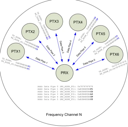
X Automatic packet transaction handling (auto ACK, auto retransmit) • 6 data pipe MultiCeiver™ for 6:1 star networks
6.2 Block diagram
Figure 4. RF Transceiver block diagram
6.3 Functional description
This section describes the different operating modes of the RF Transceiver and the parameters used to control it.
The RF Transceiver module has a built-in state machine that controls the transitions between the different operating modes.The state machine is controlled by SFR register RFCON and RF transceiver register CONFIG, see section 6.5 for details.
6.3.1 Operational Modes
You can configure the RF Transceiver to power down, standby, RX and TX mode. This section describes these modes in detail.
6.3.1.1 State diagram
The state diagram (Figure 5.) shows the operating modes of the RF Transceiver and how they function. At the end of the reset sequence the RF Transceiver enters Power Down mode. When the RF Transceiver enters Power Down mode the MCU can still control the module through the SPI and the rfcsn bit in the RFCON register.
There are three types of distinct states highlighted in the state diagram:
• Recommended operating mode: is a recommended state used during normal operation. • Possible operating mode: is a possible operating state, but is not used during normal operation.
RF Receiver ANT1 ANT2 Enhanced ShockBurst Baseband Engine TX FIFOs RX FIFOs Radio Control GFSK Modulator SPI (Slave) PA LNA TX Filter RX Filter
RF Synthesiser Power Management
RF Transmitter Baseband RFIRQ GFSK Demodulator Re gi st e r ma p RFCON.rfcken XOSC16M RFCON.rfce RFCON.rfcsn SPI (Master)
.
Figure 5. Radio control state diagram
6.3.1.2 Power down mode
In power down mode the RF Transceiver is disabled with minimal current consumption. All the register val-ues available from the SPI are maintained and the SPI can be activated. For start up times see Table 15. Power down mode is entered by setting the PWR_UP bit in the CONFIG register low.
6.3.1.3 Standby modes
Standby-I mode
By setting the PWR_UP bit in the CONFIG register to 1, the RF Transceiver enters standby-I mode.
Standby-I mode is used to minimize average current consumption while maintaining short start up times. Change to the active mode only happens if the rfce bit is enabled and when it is not enabled, the RF Transceiver
returns to standby-I mode from both the TX and RX modes. Possible operating mode
Recommended path between operating modes Possible path between operating modes Recommended operating mode
Transition state
CE = 1 Pin signal condition
PWR_DN = 1 Bit state condition
Undefined
TX FIFO empty System information Undefined Legend: Undefined Power Down Standby-I RX Mode TX Mode Standby-II RX Settling 130 us PWR_UP = 0 TX Settling 130 us TX FIFO not empty PRIM_RX = 0 rfce = 1 for more than 10µs PRIM_RX = 1
rfce = 1
rfce = 0
TX FIFO empty rfce = 1 TX FIFO not empty rfce = 1 PRIM_RX = 0 TX FIFO empty rfce = 1 PWR_UP = 0 PWR_UP = 0 PWR_UP=0 rfce = 0 PWR_UP=0 PWR_UP=0
TX finished with one packet rfce = 0
rfce = 1 TX FIFO not empty PWR_UP = 1 Start up time is 150µs Power on reset 50ms
Standby-II mode
In standby-II mode extra clock buffers are active and more current is used compared to standby-I mode. The RF Transceiver enters standby-II mode if the rfce bit is held high on a PTX operation with an empty
TX FIFO. If a new packet is downloaded to the TX FIFO, the PLL immediately starts and the packet is transmitted after the normal PLL settling delay (130µs).
The register values are maintained and the SPI can be activated during both standby modes. For start up times see Table 15.
6.3.1.4 RX mode
The RX mode is an active mode where the RF Transceiver is used as a receiver. To enter this mode, the RF Transceiver must have the PWR_UP bit, PRIM_RX bit and the rfce bit is set high.
In RX mode the receiver demodulates the signals from the RF channel, constantly presenting the demodu-lated data to the baseband protocol engine. The baseband protocol engine constantly searches for a valid packet. If a valid packet is found (by a matching address and a valid CRC) the payload of the packet is pre-sented in a vacant slot in the RX FIFOs. If the RX FIFOs are full, the received packet is discarded.
The RF Transceiver remains in RX mode until the MCU configures it to standby-I mode or power down mode. However, if the automatic protocol features (Enhanced ShockBurst™) in the baseband protocol engine are enabled, the RF Transceiver can enter other modes in order to execute the protocol. In RX mode a Received Power Detector (RPD) signal is available. The RPD is a signal that is set high when a RF signal higher than -64 dBm is detected inside the receiving frequency channel. The internal
RPD signal is filtered before presented to the RPD register. The RF signal must be present for at least 40µs
before the RPD is set high. How to use the RPD is described in Section 6.3.4 on page 33.
6.3.1.5 TX mode
The TX mode is an active mode for transmitting packets. To enter this mode, the RF Transceiver must have the PWR_UP bit set high, PRIM_RX bit set low, a payload in the TX FIFO and a high pulse on the rfce bit for more than 10µs.
The RF Transceiver stays in TX mode until it finishes transmitting a packet. If rfce = 0, RF Transceiver
returns to standby-I mode. If rfce = 1, the status of the TX FIFO determines the next action. If the TX
FIFO is not empty the RF Transceiver remains in TX mode and transmits the next packet. If the TX FIFO is empty the RF Transceiver goes into standby-II mode. The RF Transceiver transmitter PLL operates in open loop when in TX mode. It is important never to keep the RF Transceiver in TX mode for more than 4ms at a time. If the Enhanced ShockBurst™ features are enabled, RF Transceiver is never in TX mode longer than 4ms.
6.3.1.6 Operational modes configuration
The following table (Table 14.) describes how to configure the operational modes.
Table 14. RF Transceiver main modes
6.3.1.7 Timing information
The timing information in this section relates to the transitions between modes and the timing for the rfce
bit. The transition from TX mode to RX mode or vice versa is the same as the transition from the standby modes to TX mode or RX mode (130µs), as described in Table 15.
Table 15. Operational timing of RF Transceiver
Note: If VDD is turned off, the register values are lost and you must reconfigure the RF Transceiver
before entering the TX or RX modes.
Mode registerPWR_UP PRIM_RXregister rfce FIFO state
RX mode 1 1 1
-TX mode 1 0 1 Data in TX FIFO. Will empty all
lev-els in TX FIFOa.
a. If the rfce bit is held high the TX FIFO is emptied and all necessary ACK and possible retransmits
are carried out. The transmission continues as long as the TX FIFO is refilled. If the TX FIFO is empty when the rfce bit is still high, the RF Transceiver enters standby-II mode. In this mode the
transmis-sion of a packet is started as soon as the rfcsn is set high after an upload (UL) of a packet to TX
FIFO.
TX mode 1 0 Minimum 10µs
high pulse
Data in TX FIFO.Will empty one level in TX FIFOb.
b. This operating mode pulses the rfce bit high for at least 10µs. This allows one packet to transmit.
This is the normal operating mode. After the packet is transmitted, the RF Transceiver enters standby-I mode.
Standby-II 1 0 1 TX FIFO empty
Standby-I 1 - 0 No ongoing packet transmission
Power Down 0 - -
-Name RF Transceiver Max. Min. Comments
Tpd2stby Power Down Î Standby mode 150µs Tstby2a Standby modes Î TX/RX mode 130µs
Thce Minimum rfce high 10µs
Tpece2csn Delay from rfce pos. edge to rfcsn low
6.3.2 Air data rate
The air data rate is the modulated signaling rate the RF Transceiver uses when transmitting and receiving data. It can be 250kbps, 1Mbps or 2Mbps. Using lower air data rate gives better receiver sensitivity than higher air data rate. But, high air data rate gives lower average current consumption and reduced probabil-ity of on-air collisions.
The air data rate is set by the RF_DR bit in the RF_SETUP register. A transmitter and a receiver must be
programmed with the same air data rate to communicate with each other.
The RF Transceiver is fully compatible with nRF24L01. For compatibility with nRF2401A, nRF2402, nRF24E1, and nRF24E2 the air data rate must be set to 250kbps or 1Mbps.
6.3.3 RF channel frequency
The RF channel frequency determines the center of the channel used by the RF Transceiver. The channel occupies a bandwidth of less than 1MHz at 250kbps and 1Mbps and a bandwidth of less than 2MHz at 2Mbps. The RF Transceiver can operate on frequencies from 2.400GHz to 2.525GHz. The programming resolution of the RF channel frequency setting is 1MHz.
At 2Mbps the channel occupies a bandwidth wider than the resolution of the RF channel frequency setting. To ensure non-overlapping channels in 2Mbps mode, the channel spacing must be 2MHz or more. At 1Mbps and 250kbps the channel bandwidth is the same or lower than the resolution of the RF frequency. The RF channel frequency is set by the RF_CH register according to the following formula:
F0= 2400 + RF_CH MHz
You must program a transmitter and a receiver with the same RF channel frequency to communicate with each other.
6.3.4 Received Power Detector measurements
Received Power Detector (RPD), located in register 09, bit 0, triggers at received power levels above -64 dBm that are present in the RF channel you receive on. If the received power is less than -64 dBm, RDP = 0.
The RPD can be read out at any time while the RF Transceiver is in receive mode. This offers a snapshot of the current received power level in the channel. The RPD is latched whenever a packet is received or when the MCU sets rfce low
The status of RPD is correct when RX mode is enabled and after a wait time of Tstby2a +Tdelay_AGC= 130us + 40us. The RX gain varies over temperature which means that the RPD threshold also varies over temperature. The RPD threshold value is reduced by - 5dB at T = -40°C and increased by + 5dB at 85°C.
6.3.5 PA control
The PA (Power Amplifier) control is used to set the output power from the RF Transceiver power amplifier. In TX mode PA control has four programmable steps, see Table 16.
The PA control is set by the RF_PWR bits in the RF_SETUP register.
Conditions: VDD = 3.0V, VSS = 0V, TA = 27ºC, Load impedance = 15Ω+j88Ω.
Table 16. RF output power setting for the RF Transceiver
6.3.6 RX/TX control
The RX/TX control is set by PRIM_RX bit in the CONFIG register and sets the RF Transceiver in transmit/
receive.
6.4 Enhanced ShockBurst™
Enhanced ShockBurst™ is a packet based data link layer that features automatic packet assembly and timing, automatic acknowledgement and retransmissions of packets. Enhanced ShockBurst™ enables the implementation of ultra low power and high performance communication. The Enhanced ShockBurst™ features enable significant improvements of power efficiency for bi-directional and uni-directional systems, without adding complexity on the host controller side.
6.4.1 Features
The main features of Enhanced ShockBurst™ are: • 1 to 32 bytes dynamic payload length • Automatic packet handling
• Auto packet transaction handling X Auto Acknowledgement X Auto retransmit
• 6 data pipe MultiCeiver™ for 1:6 star networks
6.4.2 Enhanced ShockBurst™ overview
Enhanced ShockBurst™ uses ShockBurst™ for automatic packet handling and timing. During transmit, ShockBurst™ assembles the packet and clocks the bits in the data packet for transmission. During receive, ShockBurst™ constantly searches for a valid address in the demodulated signal. When Shock-Burst™ finds a valid address, it processes the rest of the packet and validates it by CRC. If the packet is valid the payload is moved into a vacant slot in the RX FIFOs. All high speed bit handling and timing is con-trolled by ShockBurst™.
Enhanced ShockBurst™ features automatic packet transaction handling for the easy implementation of a reliable bi-directional data link. An Enhanced ShockBurst™ packet transaction is a packet exchange between two transceivers, with one transceiver acting as the Primary Receiver (PRX) and the other trans-ceiver acting as the Primary Transmitter (PTX). An Enhanced ShockBurst™ packet transaction is always initiated by a packet transmission from the PTX, the transaction is complete when the PTX has received an
SPI RF-SETUP (RF_PWR) RF output power DC current consumption 11 0dBm 11.1mA 10 -6dBm 8.8mA 01 -12dBm 7.3 00 -18dBm 6.8mA
acknowledgment packet (ACK packet) from the PRX. The PRX can attach user data to the ACK packet enabling a bi-directional data link.
The automatic packet transaction handling works as follows:
1. You begin the transaction by transmitting a data packet from the PTX to the PRX. Enhanced ShockBurst™ automatically sets the PTX in receive mode to wait for the ACK packet. 2. If the packet is received by the PRX, Enhanced ShockBurst™ automatically assembles and
transmits an acknowledgment packet (ACK packet) to the PTX before returning to receive mode. 3. If the PTX does not receive the ACK packet immediately, Enhanced ShockBurst™ automatically
retransmits the original data packet after a programmable delay and sets the PTX in receive mode to wait for the ACK packet.
In Enhanced ShockBurst™ it is possible to configure parameters such as the maximum number of retrans-mits and the delay from one transmission to the next retransmission. All automatic handling is done without the involvement of the MCU.
6.4.3 Enhanced Shockburst™ packet format
The format of the Enhanced ShockBurst™ packet is described in this section. The Enhanced Shock-Burst™ packet contains a preamble field, address field, packet control field, payload field and a CRC field. Figure 6. shows the packet format with MSB to the left.
Figure 6. An Enhanced ShockBurst™ packet with payload (0-32 bytes)
6.4.3.1 Preamble
The preamble is a bit sequence used tosynchronize the receivers demodulator to the incoming bit stream. The preamble is one byte long and is either 01010101 or 10101010. If the first bit in the address is 1 the preamble is automatically set to 10101010 and if the first bit is 0 the preamble is automatically set to 01010101. This is done to ensure there are enough transitions in the preamble to stabilize the receiver.
6.4.3.2 Address
This is the address for the receiver. An address ensures that the correct packet is detected by the receiver. The address field can be configured to be 3, 4 or, 5 bytes long with the AW register.
Note: Addresses where the level shifts only one time (that is, 000FFFFFFF) can often be detected in noise and can give a false detection, which may give a raised Packet-Error-Rate. Addresses as a continuation of the preamble (hi-low toggling) raises the Packet-Error-Rate.
P re a m b le 1 b y te A d d re s s 3 -5 b y te 9 b it P a y lo a d 0 - 3 2 b y te C R C 1 -2 b y te P a c k e t C o n tro l F ie ld
6.4.3.3 Packet Control Field
Figure 7. shows the format of the 9 bit packet control field, MSB to the left.
Figure 7. Packet control field
The packet control field contains a 6 bit payload length field, a 2 bit PID (Packet Identity) field and a 1 bit
NO_ACK flag.
Payload length
This 6 bit field specifies the length of the payload in bytes. The length of the payload can be from 0 to 32 bytes.
Coding: 000000 = 0 byte (only used in empty ACK packets.) 100000 = 32 byte, 100001 = Don’t care. This field is only used if the Dynamic Payload Length function is enabled.
PID (Packet identification)
The 2 bit PID field is used to detect if the received packet is new or retransmitted. PID prevents the PRX operation from presenting the same payload more than once to the MCU. The PID field is incremented at the TX side for each new packet received through the SPI. The PID and CRC fields (see section 6.4.3.5 on page 37) are used by the PRX operation to determine if a packet is retransmitted or new. When several data packets are lost on the link, the PID fields may become equal to the last received PID. If a packet has the same PID as the previous packet, the RF Transceiver compares the CRC sums from both packets. If the CRC sums are also equal, the last received packet is considered a copy of the previously received packet and discarded.
No Acknowledgment flag (NO_ACK)
The Selective Auto Acknowledgement feature controls the NO_ACK flag.
This flag is only used when the auto acknowledgement feature is used. Setting the flag high, tells the receiver that the packet is not to be auto acknowledged.
6.4.3.4 Payload
The payload is the user defined content of the packet. It can be 0 to 32 bytes wide and is transmitted on-air when it is uploaded (unmodified) to the device.
Enhanced ShockBurst™ provides two alternatives for handling payload lengths; static and dynamic. The default is static payload length. With static payload length all packets between a transmitter and a receiver have the same length. Static payload length is set by the RX_PW_Px registers on the receiver side.
The payload length on the transmitter side is set by the number of bytes clocked into the TX_FIFO and must equal the value in the RX_PW_Px register on the receiver side.
NO_ACK 1bit PID 2bit
Dynamic Payload Length (DPL) is an alternative to static payload length. DPL enables the transmitter to send packets with variable payload length to the receiver. This means that for a system with different pay-load lengths it is not necessary to scale the packet length to the longest paypay-load.
With the DPL feature the nRF24L01+ can decode the payload length of the received packet automatically instead of using the RX_PW_Px registers. The MCU can read the length of the received payload by using
the R_RX_PL_WID command.
Note: Always check if the packet width reported is 32 bytes or shorter when using the
R_RX_PL_WID command. If its width is longer than 32 bytes then the packet contains errors
and must be discarded. Discard the packet by using the Flush_RX command.
In order to enable DPL the EN_DPL bit in the FEATURE register must be enabled. In RX mode the DYNPD
register must be set. A PTX that transmits to a PRX with DPL enabled must have the DPL_P0 bit in DYNPD
set.
6.4.3.5 CRC (Cyclic Redundancy Check)
The CRC is the error detection mechanism in the packet. It may either be 1 or 2 bytes and is calculated over the address, Packet Control Field and Payload.
The polynomial for 1 byte CRC is X8 + X2 + X + 1. Initial value 0xFF. The polynomial for 2 byte CRC is X16+ X12 + X5 + 1. Initial value 0xFFFF. No packet is accepted by Enhanced ShockBurst™ if the CRC fails.
6.4.4 Automatic packet assembly
The automatic packet assembly assembles the preamble, address, packet control field, payload and CRC to make a complete packet before it is transmitted.
Figure 8. Automatic packet assembly
Start:
Collect Address from TX_ADDR register
TX_ADDR MSB =1
Add preamble 0x55 Add preamble 0xAA
EN_DPL=1
PID[7:3]= #bytes in TX_FIFO Yes No Yes No SPI TX command: W_TX_PAYLOAD PID[0]=0 PID[0]=1 PID[2:1]++
Collect Payload from TX_FIFO
Calculate and add 1 Byte CRC based on Address, PID and
Payload EN_CRC = 1
CRCO = 1
Calculate and add 2 Byte CRC based on Address, PID
and Payload Yes No Yes Yes No STOP No New data in TX_FIFO REUSE_TX_PL active Yes No Yes No
6.4.5 Automatic packet disassembly
After the packet is validated, Enhanced ShockBurst™ disassembles the packet and loads the payload into the RX FIFO, and asserts the RX_DR IRQ.
Figure 9. Automatic packet disassembly
Start
PID = First byte from received bit stream
EN_DPL=1
PID[2:1] Changed from last
packet
STOP Payload = PID[7:3] bytes
from received bit stream
Payload = RX_PW_Px
bytes from received bit stream
CRCO = 1
RX_CRC = 2 Byte CRC calculated from received Address, PID and Payload TX_CRC = 2 Bytes from
received bit stream
TX_CRC = 1 Byte from received bit stream
RX_CRC = 1 Byte CRC calculated from received Address, PID and Payload
TX_CRC = RX_CRC
CRC Changed from last
packet
New packet received Yes No Yes No Yes No Yes Yes No Duplicate received No
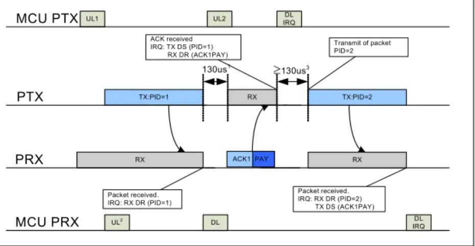
6.4.6 Automatic packet transaction handling
Enhanced ShockBurst™ features two functions for automatic packet transaction handling; auto acknowl-edgement and auto re-transmit.
6.4.6.1 Auto Acknowledgement
Auto acknowledgment is a function that automatically transmits an ACK packet to the PTX after it has received and validated a packet. The auto acknowledgement function reduces the load of the system MCU and reduces average current consumption. The Auto Acknowledgement feature is enabled by setting the
EN_AA register.
Note: If the received packet has the NO_ACK flag set, auto acknowledgement is not executed.
An ACK packet can contain an optional payload from PRX to PTX. In order to use this feature, the Dynamic Payload Length (DPL) feature must be enabled. The MCU on the PRX side has to upload the payload by clocking it into the TX FIFO by using the W_ACK_PAYLOAD command. The payload is pending
in the TX FIFO (PRX) until a new packet is received from the PTX. The RF Transceiver can have three ACK packet payloads pending in the TX FIFO (PRX) at the same time.
Figure 10. TX FIFO (PRX) with pending payloads
Figure 10. shows how the TX FIFO (PRX) is operated when handling pending ACK packet payloads. From the MCU the payload is clocked in with the W_ACK_PAYLOAD command. The address decoder and buffer
controller ensure that the payload is stored in a vacant slot in the TX FIFO (PRX). When a packet is received, the address decoder and buffer controller are notified with the PTX address. This ensures that the right payload is presented to the ACK generator.
If the TX FIFO (PRX) contains more than one payload to a PTX, payloads are handled using the first in – first out principle. The TX FIFO (PRX) is blocked if all pending payloads are addressed to a PTX where the link is lost. In this case, the MCU can flush the TX FIFO (PRX) by using the FLUSH_TX command.
In order to enable Auto Acknowledgement with payload the EN_ACK_PAY bit in the FEATURE register
must be set.
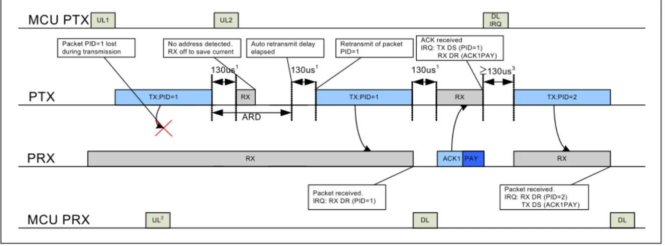
6.4.6.2 Auto Retransmission (ART)
The auto retransmission is a function that retransmits a packet if an ACK packet is not received. It is used in an auto acknowledgement system on the PTX. When a packet is not acknowledged, you can set the number of times it is allowed to retransmit by setting the ARC bits in the SETUP_RETR register. PTX enters
RX mode and waits a time period for an ACK packet each time a packet is transmitted. The amount of time the PTX is in RX mode is based on the following conditions:
TX FIFO
Payload 1 Payload 2 Payload 3
Address decoder and buffer controller
SPI Module ACK generator RX Pipe address TX Pipe address From MCU
• Auto Retransmit Delay (ARD) elapsed. • No address match within 250µs.
• After received packet (CRC correct or not) if address match within 250µs. The RF Transceiver asserts the TX_DS IRQ when the ACK packet is received.
The RF Transceiver enters standby-I mode if there is no more untransmitted data in the TX FIFO and the
rfce bit in the RFCON register is low. If the ACK packet is not received, the RF Transceiver goes back to
TX mode after a delay defined by ARD and retransmits the data. This continues until acknowledgment is received, or the maximum number of retransmits is reached.
Two packet loss counters are incremented each time a packet is lost, ARC_CNT and PLOS_CNT in the
OBSERVE_TX register. The ARC_CNT counts the number of retransmissions for the current transaction.
You reset ARC_CNT by initiating a new transaction. The PLOS_CNT counts the total number of retrans-missions since the last channel change. You reset PLOS_CNT by writing to the RF_CH register. It is
possi-ble to use the information in the OBSERVE_TX register to make an overall assessment of the channel
quality.
The ARD defines the time from the end of a transmitted packet to when a retransmit starts on the PTX. ARD is set in SETUP_RETR register in steps of 250µs. A retransmit is made if no ACK packet is received by
the PTX.
There is a restric