Design and Characterization of Selectively
Functionalized Nanoscale Electronic Devices
by Kwan Skinner
A dissertation submitted to the faculty of the University of North Carolina at Chapel Hill in partial fulfillment of the requirements for the degree of Doctor of Philosophy in the Department of Computer Science.
Chapel Hill 2008
Approved by:
Sean Washburn, Advisor
Chris Dwyer, Reader
Otto Zhou, Reader
Michael Falvo, Reader
c
2008 Kwan Skinner
ABSTRACT
KWAN SKINNER: Design and Characterization of Selectively Functionalized Nanoscale Electronic Devices.
(Under the direction of Sean Washburn.)
This dissertation is a continuation of an earlier work on the theory and fabrication
of a massively parallel self-assembled computer architecture. Specifically, this work
fo-cuses on some aspects of the fabrication of such architectures, with special focus on the
design and fabrication of the active nanoscale components of this system. To this end,
a nanoscale transistor has been fabricated and its electrical properties have been
exam-ined and improved upon. DNA-directed integration of these structures with nanoscale
scaffolds in an addressable manner via self-assembly techniques is also addressed via
a functionalization scheme that was devised to allow the arbitrary attachment of
self-assembled monolayers anywhere along the length of these nanostructures.
This dissertation also illustrates how diverse a single designed nanoscale object can
be and how the lines of chemistry, physics and materials science truly become blurred
at a scales on the order of 10−9 m. Heterostructured nanowires that were originally
only meant to act as active elements in nanoscale computer circuitry have been shown
to behave as excellent nanoscale sensors for both self-assembled monolayers (SAMs)
and gas analytes, and the same elements are now also known to act as coupling devices
for free-space photons to the surface plasmon modes of the nanowire. These sensors
enues for different uses, potentially ranging from biological applications to multiplexing
experiments.
Mechanical measurements on these heterostructured nanowires have also been
per-formed and compared quantitatively to other structures that may be chosen as
candi-dates for active or passive components a self-assembled system. These mechanical and
electrical properties can be used to make educated decisions about how components
integrated with the scaffolds to form larger computational elements will behave, and
provides essential information needed for future experiments that will produce
ACKNOWLEDGMENTS
I would first like to thank my friends and family in North Carolina, Florida,
Cal-ifornia and across the Atlantic. I sincerely appreciate all of the fun times, interesting
experiences and entertainment. You have no idea how much you helped provide me
with much needed mini-escapes when they were truly needed.
I would like to thank the my colleagues for useful and detailed conversation about
both broad ideas and specific details. Your expertise and offers of cookies have been
invaluable in coercing a Computer Scientist to come over to the Dark Side. I never
would have learned how to use half of the equipment or a fraction of the techniques I
would ultimately use while conducting this research without your help. Thank you for
sparing me a fraction of time. I only hope I have been able to repay you in some shape
or form along the way.
To the gentlemen in the machine shop and electronics lab - you have all been truly
outstanding. Thank you for teaching me how to use the machinery well enough to create
my own parts and helping me out when I couldn’t quite manage on my own during my
time here. I’d also like to thank you for repairing the many pieces of equipment used by
not only myself but others in the lab as they began to fail from wear and tear (amongst
we are familiar with instead of spending countless time and money on both purchasing
and re-learning how to use the latest and greatest.
To Bev and Maggie - thank you for making me feel welcome and handling all of the
administrative related things that us science-types are either too lazy or just no good
at handling on our own. No one could ever buy you enough flowers to deal with all of
the things you both choose to manage daily.
I would also like to thank the many people outside of my home institution that
provided support in the forms of conversation, instruction and just flat out cool
ex-periments including Dr. Thomas Mallouk at Pennsylvania State University, Dr. Ned
Seeman at New York University, and Dr. Mark Reed at Yale University.
I would also like to thank my advisor Sean Washburn for giving me a chance to
explore the fascinating and rapidly changing field of nanotechnology and letting me
tackle anything I could conjure up with my own soft tissue. A big thanks also goes to
Chris Dwyer who showed me that even the craziest (initial) ideas can come to fruition
Contents
List of Figures x
List of Abbreviations xiii
1 Introduction 1
1.1 Overview . . . 1
1.2 Thesis statement and contributions . . . 2
1.3 Outline . . . 3
2 Related work 4 2.1 State of the art computer fabrication overview . . . 4
2.2 Integration of nanotechnology now and in the future . . . 9
2.3 Self-assembled DNA scaffolds . . . 10
2.4 Nanowire fabrication . . . 11
2.5 Determination of electrical properties of semiconducting nanowires . . . 13
2.6 Nanowire mechanics . . . 16
3.2 Electroless deposition . . . 25
3.2.1 Introduction . . . 25
3.2.2 Results and discussion . . . 28
3.3 Electrochemical deposition of single-material and heterostructured nanowires 31 3.3.1 Introduction . . . 31
3.3.2 Materials and Instrumentation . . . 40
3.3.3 Experimental . . . 40
3.3.4 Formation of heterostructure nanowires . . . 43
3.3.5 Results and discussion . . . 47
4 Electrical Characteristics 60 4.1 Introduction . . . 60
4.2 Background . . . 62
4.3 Experimental . . . 67
4.4 Results & Discussion . . . 69
5 Mechanical properties of heterostructured nanowires 76 5.1 Introduction . . . 76
5.1.1 Scanning Probe Microscopy Background . . . 78
5.2 Experimental . . . 82
5.2.1 Sample preparation . . . 85
5.2.2 AFM cantilever calibration . . . 86
5.3 Results and Discussion . . . 87
6 Summary and future directions 99 6.1 Research summary and significance . . . 99
6.2 Future research directions . . . 101
A Fabrication of Thin film AAO Templates 104 A.1 Overview . . . 104
A.2 Introduction . . . 105
A.3 Experimental . . . 108
A.4 Results and Discussion . . . 109
List of Figures
2.1 A chip made using IBM’s air gap processing technology. . . 8
3.1 Top-down view of 200 nm pore PCTE membrane with embedded Au nanotubes. . . 20
3.2 AAO template with 80 nm pores. . . 21
3.3 Profile view of 200 nm Cu nanowires with Au tips still embedded in an AAO template. . . 22
3.4 Photograph of an ordered transparent mesostructured block copolymer-silica monolith. . . 23
3.5 TEM images of an AAO template with SBA-15 inside the pores. . . 24
3.6 Tilt-stage view of a 20 nm AAO template broken in half. . . 24
3.7 200 nm Au nanowires formed by electroless deposition. . . 28
3.8 SEM depicting surface roughness of 200 nm Au nanowires. . . 29
3.9 Pourbaix diagram for the system silver-water at 25◦C. . . 33
3.10 Pourbaix diagram for the system gold-water at 25◦C. . . 34
3.11 Pourbaix diagram for the system cadmium-water at 25◦C. . . 35
3.12 Pourbaix diagram for the system cadmium-water at 25◦C. . . 36
3.16 Preparation of selectively functionalized heterostructured nanowires. . . 46
3.17 High magnification scanning electron micrograph of Au nanowires formed via the electrochemical deposition of Au into AAO templates. . . 48
3.18 Tilt-stage capture of a homemade AAO broken in two and fabricated by anodization in 0.3M oxalic acid at 40 V. . . 49
3.19 Contact angle measurements of water drops on various substrates. . . . 52
3.20 Optical and bright-field micrographs of nanowires protected at specific sites, functionalized with thiolated DNA and fluorescently labeled. . . . 55
3.21 UV–visible spectra for Au nanowire/AAO composites and a blank AAO template. . . 57
4.1 SEM image of a FET based on a heterostructured a Au-CdSe-Au nanowire. 69
4.2 Experimental I −V curves of heterostructured Au-CdSe-Au nanowires. 70 4.3 ln(I) vs V plots of heterostructured nanowires at intermediate bias. . . 71
4.4 ExperimentalI-V data collected from 200 nm electrodeposited Au-CdSe-Au nanowires. . . 74
5.1 Interatomic force vs. distance curve. . . 81
5.2 Densely aggregated nanowires deposited at room temperature conditions from an ethanol solution. . . 84
5.3 Dispersed nanowires deposited from a 4 µL drop of ethanol onto a hot plate set to 160 C. . . 85
5.4 A heterostructured nanowire suspended above a chemically etched pit. 88
5.5 A broken heterostructured nanowire suspended above a chemically etched pit. . . 89
5.7 F −dcurves collected during consecutive manipulations of a single sus-pended nanowire via an AFM tip. . . 92
5.8 Suspended heterostructured nanowire after deformation beyond its point of failure. . . 94
5.9 Successive F−dcurves collected during plastic deformations on a single suspended heterostructured nanowire. . . 97
A.1 Profile view of a 55 nm pore diameter Synkera AAO template broken in half to expose the pore structure. . . 106
A.2 Thin film thermally evaporated Ti-Al layers after anodization in 0.3 M oxalic acid. . . 110
A.3 Thin film thermally evaporated Ti-Al layers with reduced surface rough-ness. . . 111
A.4 SEM micrograph at 13k of an aluminum oxide thin film anodized in 0.3M oxalic after two step anodization. . . 112
A.5 SEM micrograph at 25k of an aluminum oxide thin film anodized on glass in 0.3M oxalic after oxygen plasma treatment. . . 113
A.6 SEM micrograph at 18k of an aluminum oxide thin film anodized on glass.114
List of Abbreviations
• AAO - anodic aluminum oxide
• AFM - atomic force microscop(e/py)
• CNT - carbon nanotubes
• CV - cyclic voltammogram
• DNA - Deoxyribonucleic acid
• EIS - electrochemical impedance spectroscopy
• EUV - extreme ultraviolet
• FET - field-effect-transistor
• I-V - current-voltage
• MFM - magnetic force microscopy
• MPTMS - (3-mercaptopropyl)trimethoxysilane
• MSM - metal-semiconductor-metal
• NW - nanowire
• PCTE - polycarbonate track etched
• PMMA - poly(methyl methacrylate)
• PVP - poly(vinylpyrrolidone)
• Q1D - quasi-one-dimensional
• SAM - self-assembled monolayer
• SEM - scanning electron microscop(e/py)
• SERS - surface enhanced raman spectroscopy
• SPM - scanning probe microscopy
• STM - scanning tunneling microscopy
• TE - thermionic emission
• TEM - transmission electron microscop(e/py)
• TFE - thermionic field emission
• USD - United States Dollars
“Humanity has the stars in its future, and that future is too important to be lost
Chapter 1
Introduction
1.1
Overview
Although nanotechnology is largely in its infancy when compared to other more
established technologies, it is already finding practical use in applications ranging from
those as specific as water filtration to consumer products. In recent years, the
comput-ing and electronics industries in particular have both expressed significant interest in
integrating current developments in nanotechnology with manufacturing processes and
facilities already in place as the desire to create faster computers with higher transistor
density continues to grow. The rate of adoption of these new developments will be
largely dependent on the demonstration of their potential usefulness in end-product
applications, which will largely depend on characterization of materials properties such
as electrical, chemical and mechanical characteristics. This dissertation presents efforts
towards this goal through the design and characterization (electrically and
mechani-cally) of heterostructured nanowires which are intended for integration with nanoscale
elements in future nanoscale electronics and computing applications.
1.2
Thesis statement and contributions
This thesis presents an argument on the usefulness of heterostructured nanowires as
potential active elements in future computer circuitry. Specifically, the electrical and
mechanical properties of these structures are evaluated, and a scheme to attach different
types of molecules to different locations selectively along the length of the nanowire is
presented. In the chapters that follow, results from experiments are presented that
conveys the feasibility of these nanoscale elements to act as active and passive devices
in future self-assembled architectures.
The electrical and mechanical properties obtained from heterostructured devices
constructed here are important parameters needed when considering the functionality
desired in architectures composed of large numbers these components. Additionally, the
arbitrary attachment of various monolayers (specifically DNA) along the length of these
structures will be critical for the directed self-assembly of these systems, as traditional
write-based methods will no longer be feasible or practical. Based on the wide range
of topics addressed in this dissertation, the information here contributes directly to the
1.3
Outline
This work is organized as follows: Chapter 2 presents a brief overview of current
computer fabrication technologies and the capabilities of products produced by these
technologies in terms of feature size. A brief synopsis of self-assembled DNA lattice
technology is also included as it is anticipated to guide the assembly of smaller, future
electronic devices, along with a high-level view of the different types of nanowires and
other quasi-one-dimensional structures that have been fabricated thus far which may be
potential candidates for attaching to these lattice structures. An overview of the types
of electrical and mechanical experiments that have been conducted on these elements
is also included for completeness.
Chapter 3 presents results obtained from the fabrication of electroless and
elec-trochemically deposited single-material nanowires. An evaluation of which is more
suitable for device integration with future architectures is also presented. In
addi-tion, findings on arbitrary nanowire functionalization is also presented here, as these
functionalization schemes are expected to play a crucial role in subsequent assembly
schemes. Chapter 4 discusses the electrical characteristics of these devices, and presents
a generalized method that may be useful in the increase of majority carrier mobilities
in these devices. Chapter 5 explores the mechanical stability and robustness of these
nanostructures. Finally, chapter 6 summarizes these findings and discusses directions
Chapter 2
Related work
2.1
State of the art computer fabrication overview
Advances in processor fabrication over the last 40 years has followed a trend that
has universally been labeled as Moore’s Law. This law is frequently misquoted and
misinterpreted as the doubling of a processor’s speed and power every 18 to 24 months.
In reality, this law is in fact about the density of the number of transistors per unit
area which has no bearing on how those transistors are used in the final product.
The actual law was first summarized as follows by Gordon Moore in a 1965 issue
of Electronics Magazine well before it was formulated as a law by Caltech professor
Carver Mead and subsequently became a governing statement:
”The complexity for minimum component costs has increased at a rate of
roughly a factor of two per year...Certainly over the short term this rate can
be expected to continue, if not to increase. Over the longer term, the rate
it will not remain nearly constant for at least 10 years. That means by
1975, the number of components per integrated circuit for minimum cost
will be 65,000. I believe that such a large circuit can be built on a single
wafer.”(Gardiner, 2007)
Thus under Moore’s law, the number of transistors increase geometrically which
typically (but not always) results in double the increased performance every 18 to 24
months. Today a typical processor chip contains billions of these transistors, and these
transistors are the fundamental active elements of any processor, switching on and off
to store the logical equivalent of zeros and ones representative of data and is how basic
electronic functions are carried out.
Until recently, this increase in transistor density has been almost uniformly obtained
by advances in the photolithographic processes used to create these structures on a
chip, which has resulted in smaller and smaller features packed more and more closely
together. Decreases in the size of transistors on a chip both increases the speed a chip
can operate and the amount of data that can be stored while simultaneously resulting
in a decrease in the manufacturing cost. To date, the most advanced chips have features
as small as 65 nanometers. The next major milestone is a decrease in this feature size
to 45 nanometers, but simply shrinking the feature size, which is a formidable task
in itself, is not sufficient because at this scale crosstalk, or the undesirable leakage of
electrical current from a transistor between parallel lines in a circuit, is considerable.
This can cause signals that are supposed to represent a logical one flip to a zero and vice
Chipmakers including Intel, IBM and Texas Instruments are now taking measures
to address this by replacing silicon and silicon dioxide, the materials that have been
the backbone of the information age for over the last 40 years, with newer materials
such as hafnium to help minimize this leakage of electrical current. Intel states that the
adoption of this new material, along with a couple of others that have yet to be disclosed,
will allow the company to double the number of processors while still occupying the
same amount of space.(Greene, 2007a) This will permit future chip designers with the
option of either boosting the number of processors per chip to make chips faster, or
reducing the footprint of their current chips by squeezing the same chip designs into a
smaller space and reducing their manufacturing costs.
The other major limitation in the determination of the size of features definable on
a chip aside from the materials used is due to the lithography used to create features
themselves. The tools used for lithography make use of a light source and a collection
of lenses and mirrors along with a transparent mask to define patterns on a silicon
wafter that will ultimately house the chip. This imprint defined by the light source and
the mask permits different materials to be deposited onto the surface in different places
through a series of chemical reactions, much like light forms images on unexposed film.
The tool used to create these features currently has a price tag in the neighborhood of
$15m.(Spooner, 2004)
The latest lithography tools planned for use by Intel uses lenses and filters along
with a ultraviolet (UV) light source to define these features on a silicon wafer. Their
nm, although their current processes use a light source with a wavelength of 193 nm
but can produce features as small as 50 nm. This setup will be used until 2009, after
which the newer light source will replace the current source to produce features as small
as 32 nm.
The price tag of the facilities that house these tools increase drastically with every
decrease in feature size. The latest plant designated for construction by Intel is located
in China and will cost them some 2.5b USD and is expected to enter production in
2010.(Lemon, 2007)(infoworld) This plant won’t even be considered ‘state of the art’
once it finally does enter production. Intel’s ’fab32’ facility, which is supposed to house
the technology used to produce features that are 32 nm in size and will be located in
Arizona, is slated to cost over 3b USD.(Jade, 2005)
As the cost continues to creep higher and higher, manufacturers seek out new
tech-nologies to aid in both keeping costs down while simultaneously allowing them to
ad-here closely to Moore’s Law. Current toolsets will permit them to follow Moore’s
law for several more years, but engineers are increasingly understanding the need to
switch to new materials and designs to allow these trends to continue into the future.
In particular, manufactures are investing considerable research and development
ef-forts into using nanotechnology to allow them to continue adhering to the trends that
produce products and advances consumers have enjoyed for decades. Present-day
re-search in the integration of new materials include efforts in growing carbon nanotubes
(CNTs) and nanowires (NWs) directly onto silicon wafers.(Hwang et al., 2005) IBM has
wiring.(McConnel, 2007) These foams are then later removed and a vacuum is left in
place as the dielectric material insulating individual gates from one another, and
pre-venting crosstalk. This technique allows chip speeds to be increased by an additional
35% or permits a decrease in the power requirements by 15%. (You can choose one or
the other, but not both.)
2.2
Integration of nanotechnology now and in the
future
Although considerable efforts are now being placed into researching various areas
for new materials and design adoption, the use of CMOS or CMOS-like transistors is
expected to come to an as early as 2020 when transistors literally consist of only a
few atoms, making it literally impossible to shrink them any further.(Kurzweil, 2000)
Currently some of the most promising ideas that may eventually permit this level of
miniaturization include spintronics(Engel and Loss, 2005) where electrons themselves
store the state of a one or zero and materials that exhibit a change in the state of
the phase of the material itself stores its contents(Agarwal, 2007). Optical technology
using photonics is also shaping up to be another viable candidate, where the presence
or absence of light itself stores the representative zero or one.(Barrelet et al., 2004;
Sanders et al., 2006)
In the more foreseeable future, less radical paths are likely to be adopted. This is
likely to be witnessed in the form of the integration of nanotechnology with current
fabrication processes instead of complete and total replacement of current silicon-based
technologies with nanotechnologies. Evidence of this can presently be seen in the
integration of monodisperse nanocrystals with silicon wafer technology to produce
non-volatile flash memories that use lower power and have higher write-erase life cycles.
(Greene, 2007b)
DNA as possible structures that can eventually be integrated with current CMOS
technology to extend its lifetime, and possibly even replace it entirely for certain
ap-plications. These structures look to the very core of biology to assemble predictable
structures from the material that defines life itself due to the specificity of
Watson-Crick base pairing.(Dwyer, 2003; Pease et al., 1994; Fu and Seeman, 1993; Cook et al.,
2004) To date various structures and patterns have been self-assembled including some
with spacings as small as 20 nm that are fully addressible.(Park et al., 2006) Computer
architectures have also been proposed to make use of these structures and considerable
headway has already been made in both preliminary theoretical designs and
experi-mental implementation.(Kuekes et al., 2005; Han and Jonker, 2003; Cook et al., 2004)
In order to function as useful computational devices, these architectures will require
the design of fundamentally different active elements, or transistors.
2.3
Self-assembled DNA scaffolds
Self-assembled nanostructures composed of DNA were first formulated by Seeman in
1982.(Seeman, 1982) Structures formed from DNA generally make use of one or more
re-peating base units that are then self-assembled into larger, regularly patterned lattices.
These base units include triangles(Chelyapov et al., 2004; Liu et al., 2003), squares(Park
et al., 2006), psuedo-hexagons (Ding et al., 2004) , six-helix bundles(Mathieu et al.,
2005), six-point stars(He et al., 2006) and parallelograms(Mao et al., 1999) – all of
with single crystals being as large as 200 µm(He et al., 2006) . Rothemund has even
managed to coerce single kilobase strands of DNA into intricate shapes and patterns
by exploiting the self-assembly properties of DNA via what has been labeled ‘DNA
origami’.(Rothemund, 2006)
The general consensus to date supports the use of a multi-step fabrication process
for the production of architectures produced by these type of self-assembly schemes.
The assembly of the scaffolds themselves may or may not require multiple steps,
de-pending on the complexity of the target structure and whether the route adopted for
self-assembly makes use of a single assembly step or a hierarchal method. Useful
prod-ucts yielded from self-assembly will require the attachment of other types of materials
to specific points on the lattices. This is evident in the preliminary architectures
pro-duced by several groups that produce the scaffolds first followed by the attachment of
nanoparticles or other similarly sized objects such as viruses(Zhang et al., 2006a; Park
et al., 2006; Sharma et al., 2006). Ultimately, these nanoparticles will likely be replaced
by more useful structures, loosely known as ‘nanowires’, in order to begin mimicking
the circuits produced by lithography today.
2.4
Nanowire fabrication
Some of the very first nanostructures that are now universally labeled as ‘nanowires’
were controllably produced by Possin and reported on in 1970.(Possin, 1970) His
dimen-sions roughly 40 nm wide and 15µm long. This method helped lay the groundwork for
what would later become known as templated nanowire deposition which involves using
a sacrificial template to confine one dimension of the nanowires while the other
dimen-sion (the length) is variable and determined by the nanowire growth/deposition time.
The template method is still widely used today (Kline et al., 2006; Riveros et al., 2005;
Nicewarner-Pena et al., 2001) but mica has generally been replaced by anodic aluminum
oxide (AAO) templates(Nielsch et al., 2001; Schonenberger et al., 1997),
polycarbon-ate templpolycarbon-ates(Schonenberger et al., 1997) and in some instances even composite or
silica based templates(Lu et al., 2004). Template based methods (and in particular
nanowires grown in AAO templates) have several advantages over other nanowire
fab-rication methods including tight control over the diameters of the nanowires and as
it will be demonstrated later, control over the location of functional groups on the
surfaces of template grown nanowires. Nanowires capable of being produced inside of
templates include both conducting(Yu et al., 1997) and semiconducting(Zheng et al.,
2001) structures, and the template method has even been used to grow CNTs(Hwang
et al., 2005).
Other methods employed in the fabrication of nanowires include solution based
routes which don’t require the presence of a negative template at all. In some
in-stances, DNA itself has even been use as a positive template for the attachment of small
nanoparticles including nanoparticles made of platinum(Gill et al., 2000), silver(Braun
et al., 1998), gold (Patolsky et al., 2002), palladium(Deng and Mao, 2003) and
this method usually have diameters of several tens of nanometers, and the variation in
the diameter over the length of the nanowire is usually non-uniform and non-negligible.
Vapor deposition methods (CVD, VLS) may also used to produce nanowires with
di-ameters consistently less than 100 nm. Nanowires produced by vapor methods include
GaO (Song et al., 2004), germanium(Greytak et al., 2004) and ZnO(Song et al., 2005)
which have all been produced by VLS, and ZnO(Ng et al., 2004), (Fan et al., 2004)
pro-duced by CVD. Thermal evaporation has even been used to produce nanowires without
a template.(Byon et al., 2005) Core-shell and vertical gate structures have been
pro-duced by vapor methods as well.(Ng et al., 2004),(Lauhon et al., 2002) Other methods
include routes which make use of surfactants(Grebinski et al., 2004) and routes that
are surfactant–free(Shao et al., 2004) to produce both straight and branched nanowire
structures.
2.5
Determination of electrical properties of
semi-conducting nanowires
The electrical properties of individual nanowires have undergone significant study
over the past several years and it has been found that characteristics such as majority
carrier mobility of these structures almost always varies drastically from bulk values
due to large differences in surface to volume ratios of the bulk materials and the
quasi-one-dimensional equivalent shapes that are nanowires. Researchers usually attribute
density in the conduction channel to the surface of these nanostructures due to applied
biases, where an increase in the scattering probability results in a degradation of the
electron mobility.(Kolmakov and Moskovits, 2004) For instance, the bulk value for the
majority carrier mobility of CdS is 340.0 cm2 V−1 s−1 but the mobility reported in a
nanowire with a diameter on the order of 100 nm is an order of magnitude lower at 32.20
cm2 V−1 s−1.(Zhang et al., 2006b) As such, it is generally true that observations of elec-trical properties made for bulk materials don’t readily apply to nanoscale structures.
One method of extracting properties such as the bulk mobility from these structures
involves depositing already constructed nanowires onto a silicon/silicon oxide substrate
from solution and forming contacts to individual nanowires via lithography.(Williams
et al., 2003) The nanowires can then be individually addressed and its conductance
can be modulated by using the substrate as a global gate.(Huang et al., 2001)
Lo-cal gates can also be defined lithographiLo-cally as a top(Lauhon et al., 2002) or lateral
gate(Clement et al., 2002) or through other nanowires themselves.(Huang et al., 2001)
The conductivity of individual nanowires has also been gated through the generation of
a photocurrent by illuminating optoelectronic structures with light.(Pena et al., 2002)
The use of any of these geometries results in modulation of the semiconducting
chan-nel of these nanowires and the electrical properties can be investigated accordingly
and parameters can be extracted including the transconductance, carrier mobility, and
number of donors. In addition, there have been several studies conducted on bundles of
nanowires in order to observe the electrical properties of these structures as well.(Pena
Electrical characterization of nanoscale structures has also been performed through
other methods, although these techniques tend to be used less than conventional
lithog-raphy methods due to the amount of information any one technique is generally capable
of yielding. For example, uv-vis spectra are often collected for nanostructures in
or-der to determine the optical bandgap since the absorption peak is dependent on the
bandgap energy of the underlying structure and for smaller structures on quantum
confinement.(Kwak et al., 2007) Electrochemical impedance spectroscopy (EIS)(Beach
et al., 2003) is a method that can detect the capacitance of the depletion region of a
semiconductor by using an electrochemical cell and a suitable electrolyte such as a pH
buffer. An equivalent circuit is selected after collecting the data, and the spectroscopy
data can be used to determine the values of various components of the circuit. The
capacitance can be extracted, and this can be used to construct a Mott–Schottky plot
in order to determine the carrier density of the semiconductor under investigation. As
such, EIS can give information about band-edge potentials.(Beach et al., 2003;
Mora-Sero et al., 2006; Bisquert, 2008) Additionally, photocurrent measurements can also
provide information about the band-edge potential of the material, and the material
type can also be determined by monitoring anodic or cathodic currents.(Wang and Tao,
2007) While each of these methods can yield valuable information about the structures
under investigation, no single method is capable of providing the amount of information
that can be obtained from electrical measurements that yield ‘standard’ current–voltage
(I–V) curves. The information that can be extracted from these data include but are
type (n–type or p–type), gate threshold voltage, majority carrier concentration and
information about the contact barrier height established between the metal electrodes
and semiconductor nanowire.
2.6
Nanowire mechanics
In comparison to the amount of information available on the electrical properties of
nanostructures, the information available on the mechanical nature of these structures
is relatively scarce. The tool of choice for these types of investigations is typically the
atomic force microscope (AFM) since it allows direct manipulation of the structures of
interest. Vertically aligned nanowires of ZnO have been investigated with this method in
order to determine the elastic modulus(Song et al., 2005) as well as the fracture strength
and Young’s modulus(Hoffmann et al., 2007). Mechanical measurements have also been
performed on nanowires anchored down to a substrate and suspended horizontally
across predefined trenches.(Wu et al., 2005)(Wu et al., 2006) The Young’s modulus
and yield strength were both determined for structures in this configuration, and the
Young’s modulus was found to be independent of the nanowire diameter and the speed
at which the cantilever performed the manipulation on the nanowire. Other groups
have used SEM(Yu et al., 2005)(Dikin et al., 2003) and TEM(Wang et al., 2002; Wang,
2003; Wang et al., 2001) instruments to determine the bending modulus of quasi–one–
dimensional nanostructures via electron beam and field induced actuation. Thermally
Chapter 3
Selective Functionalization of
Nanowires
3.1
Nanowire construction overview
Over the past few years, a large number of nanoscale devices have presented
them-selves as candidates to serve as fundamental elements in both future nanoscale systems
and computational devices. These candidates have included carbon nanotubes
(Bach-told et al., 2001) and nanowires fabricated from various materials.(Fan et al., 2004;
Kovtyukhova et al., 2004; Byon et al., 2005) Nanowires are one type of several
quasi-one-dimensional (Q1D) structures that have large aspect ratios and can be produced
from porous alumina (PA) templates with diameters within the range of one to several
hundred nanometers. Various methods are presently in use that allows for the
fabri-cation of these structures including chemical vapor deposition (Greytak et al., 2004),
solution-based methods(Mitamura et al., 2007), lithography(Koops et al., 1995),
template based deposition.(Pena et al., 2002; Nicewarner-Pena et al., 2001)
The template fabrication method allows for the diameters of the nanowires to be
defined by the size of the pores in the template. Because various sets of parameters
including the anodization voltage, the electrolyte temperature and the anodization
acid used will produce different pore sizes in these templates, the resulting nanowires
have diameters ranging from several hundred nanometers down to 8 nm or less.(Wade
and Wegrowe, 2005) Thus, the size and size distribution of the nanowires are directly
determined by the size and the size distribution of the pores of the template. The
length of the nanowires produced in the template is determined by the amount of time
the material constituting the nanowires is deposited and also by the rate of deposition.
Additionally, the material deposited is adjustable as well. This feature is unique to
the template based deposition that is not easily controllable in methods that involve
solution based growth and therefore template deposited nanowires can be produced
with arbitrarily varying material composition along the length of the nanowire simply by
varying the composition of the plating bath. Nanowires constructed from templates are
generally formed in templates one or more of three different materials: polycarbonate
track-etched membranes (PCTE), anodic aluminum oxide (AAO) which are also known
as porous alumina (PA) templates , or the so-called SBA-15 materials. Each has its
benefits which will briefly be outlined here.
PCTE membranes are flexible membranes that have nano and micro-sized pores
that have been formed through a technique known as the ‘track etching’. This method
cylin-drical tracks to be left in the irradiated foil due to energy loss of the ions as they
inter-act with the foil.(Schuchert et al., 2003) These tracks can then be widened by chemical
etching, and can produce uniform pores of arbitrary sizes as long as the energy of
the heavy ions bombarding the PCTE membrane is sufficient. The main benefits of
these templates is their flexibility, which allows for easy handling, and the ability to
roughly control the average spacing between pores (c.a. AAO membranes which have
pores that are packed a lot more closely). The main disadvantages of these templates
includes their inability to withstand high processing temperatures, the random
distri-bution of the placement of the pores on the surface, and the non-parallel orientation of
the pores with respect to each other which results in some pores crossing with others,
and causes any material deposited within these joined pores to appear as one misshaped
nanowire instead of two separate entities.
AAO templates are ceramic materials with a closely packed and hexagonally ordered
pore structure. The pores can have sizes ranging from 7 or 8 nanometers up to a couple
of hundred.(Wade and Wegrowe, 2005) These templates are formed by the
electrochem-ical anodization of aluminum foil in acidic conditions. Typelectrochem-ically, a piece of polished,
high-purity aluminum foil is placed as one electrode in an anodization bath while in
the presence of another electrode. A voltage is set between the two electrodes, and the
metallic aluminum foil is slowly converted into a porous aluminum oxide. Both the
composition and the temperature of the bath determine the size of the pores formed,
and the thickness of the aluminum oxide sheet is determined by the anodization time.
Figure 3.1: Top-down view of 200 nm pore PCTE membrane with embedded Au nanotubes.
film, depending on whether an aluminum oxide template is preferred with
through-holes (like the PCTE membranes described above) or whether one wishes to leave the
template attached to the original aluminum foil support. Nanowires can be produced
in both of these templates in either case.
A third type of template that is relatively new but is gaining much attention are the
so-called SBA-15 templates. These mesoporous materials are a special class of
nano-materials with ordered nanopores with pore sizes between 3 and 30 nm.(Yang et al.,
Figure 3.2: AAO template with 80 nm pores.
requiring high-density but separated nanowire arrays.(Lu et al., 2004) These block
copolymer-silica structures are formed through a sol-gel method, and because this
ma-terial faithfully replicates the vessel the reaction is carried out in, different templates
can be used for the production of this material including AAO templates. Figure 3.4
contains a 4.8 cm long by 2.1 cm wide by 0.2 cm sample of the ordered transparent
mesostructured block copolymer-silica that has been removed from its mold, and
Fig-ure 3.5 contains the block copolymer that has taken the shape of 200 nm nanowires as
Figure 3.3: Profile view of 200 nm Cu nanowires with Au tips still embedded in an AAO template.
Unless otherwise stated, the nanowires that are referenced throughout this
dis-sertation are constructed from commercial AAO templates and were fabricated via
electrochemical deposition techniques. Specifically, the AAO templates used here were
primarily the Anodisc variety obtained from Whatman, Inc. and contained 200 nm
pores. It is important to note that although the rated pore sizes of the AAO template
is 200 nm, the actual pore sizes tyically range between 200 and 350 nm depending on
the individual template. The sizes of the pores of the templates used here refer to
Figure 3.4: Photograph of an ordered transparent mesostructured block copolymer-silica monolith. Taken from (Yang et al., 2003)
themselves. Although this manufacturer also sells AAO templates with pore sizes of
100 nm and 20 nm, it was discovered that the diameters of the pores were not uniform
throughout the 60 µm thickness of the entire template. Figure 3.6 is an SEM
micro-graph of one of the 20 nm Anodisc templates that has been broken into two in order
to show the non-constant diameter of the pores. The pores start out with diameters
of 20 nm (upper portion of image), but quickly changes to larger dimensions and the
remainder of the length of the pores assumes a pore size comparable to the 200 nm
Figure 3.5: TEM images of an AAO template with SBA-15 inside the pores. Taken from (Lu et al., 2004)
Figure 3.6: Tilt-stage view of a 20 nm AAO template broken in half. The 200
a few hundred nanometers, these templates were not usable for depositing nanowires
for the majority of the experiments performed here and resulted in considerable effort
being devoted to fabricating templates of these dimensions in house. Fortunately, a
dif-ferent manufacturer, Synkera Technologies, began producing their own templates with
similar macroscopic dimensions to address this very problem, and templates with pores
as small as 13 nm have been routinely acquired from them for experiments conducted
for the growth of nanowires for the attachment to DNA lattices.
3.2
Electroless deposition of single material nanowires
3.2.1
Introduction
The electroless deposition of metal onto a surface involves the reduction of a metal
ions in solution using a chemical reducing agent. Because the substrate does not have
to be conductive, one advantage of this method over electrochemical methods is that
the substrates often require no special preparation for conductivity purposes before
use. The main requirement of this method, however, is that the transfer of electrons
from the reducing agent to the metallic ions in solution is slow, which prevents the bulk
reduction of the metal in solution all at once. Additionally, if a catalyst is placed on
the surface of substrate of interest, reduction will preferentially take place here and not
on other surfaces accessible to the reduction medium.
The electroless chemistry used in this paper is a slight modification of the method
are often coated with poly(vinylpyrrolidone) (PVP) in order to promote wetting of
the pores when immersed in aqueous solvents (these membranes are intended for use
as filtration devices, after all). This deposition technique involves using a sensitizer
(Sn2+) that binds to PVP in order to coat the surface of the membrane with a metal since PVP contains metal-complexing amine and and carbonyl groups. The surface is
then activated with ammoniacal silver nitrate which causes Sn(II) to be oxidized to
Sn(IV), and the Ag+is reduced to elemental Ag and coats the surface of the membrane with nanoscopic particles of Ag. The membrane is then placed in a plating bath of Au,
which causes the Ag particles to be galvanically replaced with Au particles since Au
is a more noble metal. These particles then act as catalytic sites for the oxidation of
formaldehyde and the subsequent reduction of Au(I) to Au(0).
As far as is known, this work contains the first instance of 200 nm Au nanowires
formed in PCTE membranes based on electroless chemistry (see Figure 3.7). The
mod-ifications made to Menon and Martin’s procedure was necessary due to the formation
of nanotubes instead of nanowires. Namely, if the concentration of the Au plating bath
is insufficient for filling all of the pores of the membrane nanotubes will form instead
of nanowires since the deposition of Au proceeds beginning at the surface of the pores
in the membrane. The inner diameter of these tubes can be controlled either by the
amount of Au present in the plating solution or by limiting the amount of time the
3.2.1.1 Experimental
The fabrication of 200 nm nanowires in PCTE membranes is initiated with the
preparation of the Sn sensitizer solution, which was composed of 0.026M SnCl2 and 0.07M trifluroacetic acid, with a solvent of 50/50 methanol/water. The PCTE
mem-brane was immersed in this solution for 3 min, and the memmem-brane was then rinsed
with 3 times with large quantities of methanol. The Sn2+ coated membrane was then activated with a 0.029M solution of ammoniacal silver nitrate. The membrane was
then rinsed in 2 times with copious quantities of methanol and then placed in distilled
water. For the final step, the Ag coated membrane was placed in a reduction bath
containing 1.2 x 10⁻¹M Na3Au(SO3)2 (the commercial plating solution of Oromerse Part B diluted with distilled water), 0.127 M Na2SO3 and 0.625 M formaldehyde which had been chilled to ˜2◦C before adding the formaldehyde as its addition will cause
the deposition reaction to commence immediately. The plating of Au onto the PCTE
membrane proceeded overnight (typically about 18 - 24 hours) and was removed from
the plating solution and rinsed with water and methanol before being air dried under
a stream of nitrogen.
Menon and Martin were able to gain access to the nanowires formed in the PCTE
membranes by applying tape to the surface of the membrane and then removing it,
causing the thin film of metal formed on the surface of the membrane to be removed
with the tape and providing access to the nanowires themselves. This was applicable for
their samples since the amount of metal deposited on the surfaces of their templates was
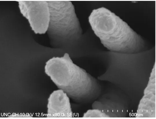
Figure 3.7: 200 nm Au nanowires formed by electroless deposition. Nanowires with oblong tips result from removing the gold layer coating the entire surface of the membrane in order to gain access to the nanowires themselves.
excess of 100 nm, and lengths on the order of 10 µm, which is defined by the thickness
of the template. Any attempts in removing the layer of metal deposited on the surface
of the membrane resulted in only a thin surface layer of the metal being removed.
Repeated applications of the tape would eventually cause the membrane itself to tear.
3.2.2
Results and discussion
Due to the thickness of the metal layer, the most straightforward method of gaining
access to the nanowires was to apply ample pressure to the surface of the membrane
Figure 3.8: High magnification SEM of 200 nm Au nanowires showing the amount of surface roughness.
the membrane as the metal layer was removed. Unfortunately, the amount of pressure
applied to the surface of the membrane while wiping also induces large amounts of
sheer stress on the membrane itself, and causes the nanowires within the membrane to
undergo sheer stress as well. This results in bent tips at the ends of the nanowires as seen
as elongated tips appearing as ellipsoids on some of the ends of the nanowires as seen in
Figure 3.7, and immediately makes them less usable if quasi one-dimensional structures
are desired as this process introduces an asymmetry into the physical structure of the
nanowire.
Additionally, Figure 3.8 clearly shows the amount of surface roughness present on
walls of the PCTE membrane pores themselves are relatively smooth.(Nasirpouri et al.,
2007) The roughness present in the nanowires here likely results from the rate that the
reaction occurs during the initial moments of the electroless deposition process. A
change in the kinetics of the reaction such that the reaction is slowed down may allow
for the formation of smoother surfaces of the deposited nanowires.
The nanowires seen in both Figure 3.7 and 3.8 have had a portion of the surface
of the PCTE membrane removed by ozone plasma etching,(Yu et al., 2003) which was
achieved by placing the PCTE membrane into the chamber of an oxygen plasma cleaner.
This process of separating the template from the nanowires is relatively slow, requiring
15 minutes of etching at 100W to remove a couple of microns of the template-based
on previously conducted experiments. Figure 3.7 also shows two separate pores that
are in close enough proximity that what should have been individual nanowires have
coalesced into one; a problem that is common with these types of porous membranes
unless the density of the tracks created by heavy ion bombardment is sufficiently low
enough that the probability of two ions creating two separate tracks in close proximity
is sufficiently small. This however significantly decreases the density of the number of
nanowires that can be created, and therefore is not desirable for applications that wish
to make use of massively parallel device construction routines.
In terms of cost, the electroless deposition route is also somewhat wasteful, as a
significant amount of the metal being reduced is also deposited non-specifically on the
outer surfaces of the PCTE membrane as well as on the surface of the vessel the reaction
the nanowires produced in the PCTE membranes (which is determined by the thickness
of the membrane itself) resulted in alternate methods to be sought out.
3.3
Electrochemical deposition of single-material and
heterostructured nanowires
3.3.1
Introduction
Electrochemical deposition is the general process describing the reduction of metal
or semi-metal ions from solution onto a conducting substrate. The general conditions
required for this to occur includes a solution of the proper composition (material,
concentration, pH, etc.) and a potential of the appropriate magnitude applied between
two conducting electrodes in solution, one of which being the electrode that is to be
the target for the deposition of metal. The general reaction for this process is
Mz++ ze− ←→M(s). (3.1)
When the necessary conditions are satisfied, namely when the proper potential is
applied between the two electrodes in solution and the proper pH conditions exist,
the result is a metallic or semi-metallic precipitate formed on the cathode (i.e. working
electrode) of the experimental setup. Thus the ions of interest in solution can be reduced
from solution onto the electrode in the presence of a sufficient potential between the
between the working electrode and the solution is more negative than the potential
difference at equilibrium conditions Ueq when no net reaction occurs. The opposite is true as well, and when the potential difference between the working electrode and the
plating solution is larger than Ueq, deposited metal will be dissolved since the ionic form is favorable.
A quick assessment of the deposition conditions that will permit the reduction of
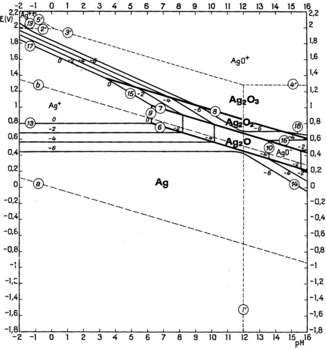
the material of interest from solution can be determined from a Pourbaix diagram.
These diagrams are mappings of pH-U space that shows which phases are
thermody-namically stable for a pH and potential of interest. Ion boundaries are represented
by lines indicating the stable phase, and these diagrams can be read much like phase
diagrams. Figures 3.9, 3.10, and 3.11 contain the Pourbaix diagrams for Ag, Au and
Cd respectively; materials that were all used in the construction of the nanowires to
be discussed in this section. These diagrams show that the ionic phase of these metals
are only stable over certain pH and potential ranges. For example, from Figure 3.10
we can see that at a pH of 6 gold oxide forms at potentials above 1.2 V. When we also
consider the boundary between where water is stable and the liberation of hydrogen
occurs in Figure 3.12, we see that hydrogen evolution occurs over most of the potential
range where Au deposition also takes place.
The pourbaix diagrams included here are only rough indicators of the conditions
required for the successful reduction of metallic ions onto an electrode. Optimization
of these conditions requires a cyclic voltammogram (CV) to be performed for each
Figure 3.12: Pourbaix diagram for the system cadmium-water at 25◦C.
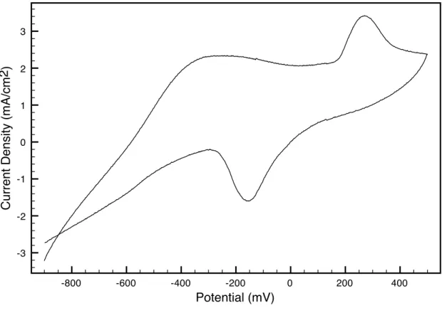
of the kinetics of the system during electrodeposition. As is evident in figure 3.13,
an increase in electrodeposition current occurs as a more negative potential is applied.
At sufficiently large current densities, the reaction becomes rate limited by diffusion.
In aqueous solutions, hydrogen evolution is also a byproduct of increasingly negative
potentials. The local minima of this reduction peak denotes where deposition of the
electroactive species in solution begins, and any value at this peak or lower may be
chosen for electrodeposition as long as hydrogen evolution is considered when depositing
at more negative potentials.
All of the CVs in Figures 3.13 – 3.15 were collected using 200 nm AAO templates.
Analysis of these CVs allows one to determine a range of appropriate potentials to use
for the deposition of the metal of interest from solution. For the silver and gold ion
-800 -600 -400 -200 0 200 400
Potential (mV)
-3 -2 -1 0 1 2 3
Current Density (mA/cm
2)
Figure 3.13: Cyclic voltammogram of Ag deposited into a metal-backed AAO template. Potential referred to reference electrode.
the deposition of CdSe, the potential was alternated between -350 and -800 mV based
on analysis of the cathodic scan of the cycle in the cyclic voltammogram collected for
this electrolyte, which is well correlated with potential deposition ranges suggested in
literature by Kressin.(Kressin et al., 1991) A binary semiconductor of near
stoichiomet-ric proportions is desired and can be produced by depositing CdSe in equal proportions.
At a potential of -350 mV, CdSe and Se is deposited at rates equal to or less than the
diffusion limited rate in submonolayer quantities (for CdSe) and far less for Se based
on the rate of deposition which is determined by the concentration of the species in
-800 -600 -400 -200 0 200 400 Potential (mV)
-6 -4 -2 0 2 4 6
Current Density (mA/cm
2)
Figure 3.14: Cyclic voltammogram of Au deposited into a metal-backed AAO template. Potential referred to reference electrode.
mV) bulk Cd is deposited in excess during the remainder of the cathodic scan. The
Cd that has not reacted with selenium is then stripped off, which corresponds to the
oxidative peak present in the anodic portion of the scan located at roughly -350 mV in
the CV. Given the deposited CdSe is thermodynamically stable enough, it remains on
the surface and the next cycle is initiated, resulting in the gradual deposition of CdSe,
which proceeds at 7 ˚A/s.(Kressin et al., 1991)
It’s important to keep in mind that the reduction of Au and Ag from solution at -1
-800 -600 -400 -200 0 200 400
Potential (mV)
-15 -10 -5 0 5 10 15
Current Density (mA/cm
2)
Figure 3.15: Cyclic voltammogram of CdSe deposited into a metal-backed AAO template. Potential referred to reference electrode.
used for the reduction of the ions present in solution and needs to be accounted for when
monitoring the coulombs of charge passed through the cell when depositing nanowires,
as the apparent length will routinely fall short of any theoretical values determined that
do not take hydrogen evolution into consideration. The single material nanowires used
here are generally composed of Au, and as such these will be the nanowires focused on
3.3.2
Materials and Instrumentation
A commercial potentiostat (PST050, Radiometer Analytical) is used to
electro-chemically deposit the nanowires into the template with a Pt counter electrode and a
Ag/AgCl (sat KCl) reference electrode. Ag plating solution (Silver 1025, Technic Inc.)
and Au plating solution (Orotemp 24, Technic Inc.) were obtained from the respective
manufacturers. NaOH, ethanol (Fisher Scientific) and HNO3 were all obtained from
Fisher Scientific. Contact angle measurements were obtained using a CCD camera
and a home-made XYZ positioning stage. High purity aluminum (Alfa Aesar, 99.998%
pure, 0.5 mm thick) was also obtained from Fisher Scientific.
3.3.3
Experimental
3.3.3.1 Preparation of AAO templates for electrochemical deposition of metallic ions from solution
The preparation of the AAO templates used for the electrochemical deposition of
metals inside the pores begins with the thermal evaporation of Ag onto one side of the
template. A special metal sheet with nine holes slightly larger than the dimensions of
the AAO templates themselves (13 mm in diameter) except for a small segment at the
bottom with dimensions of 12 mm in diameter is used as a holder for the templates
in the thermal evaporation chamber and was fabricated in house by the machine shop.
The holder is suspended from a standard sample stage at an angle using clips and
covers the holes and allowed us to skip the step performed by others(Yu et al., 2000)
of electrochemically depositing more Ag onto the backside of the template before the
actual nanowires are deposited.
The AAO templates are placed shiny side down into the template holder before it is
suspended from the sample stage. This side of the AAO template is often referred to as
the branched side as the pores here do not typically run parallel to each other and are
interconnected, which is likely a by-product of the deposition method used to separate
the alumina templates from their underlying aluminum substrates.(Routkevitch et al.,
1996)(Jessensky et al., 1998)(Tian et al., 2005) This orientation is chosen to facilitate
the electrochemical deposition of Ag, which allows the rest of the template to be filled
with the metal of choice while generally not having to be concerned with more branching
at a later segment of the channel.
Metal is typically evaporated onto the substrates at a rate between 5 and 50 nm/s.
Performing the evaporation at a lower rate did not appear to have any noticeable
ben-efits, as this layer is only meant to serve as a conducting layer permitting the template
to be an electrically active component in the series of components that comprise the
circuit that defines the cell while being consistent (i.e. non-porous) enough to
pro-vide a good base substrate for the electrochemical deposition of additional metal into
the pores of the template itself. The prepared templates are stored in a container at
atmospheric conditions until further used.
The prepared AAO templates are placed into the electrochemical cell with the
and then filled with Ag plating solution. The Ag layer deposited here is used as a
sacrificial layer as the bottoms of the AAO pores are not parallel and exhibit significant
branching. Deposition was performed by using the chrono coulometry method of the
Voltalab software. The deposition was performed at -1 V and was allowed to proceed
until -2 C of charge was passed through the cell based on the integration of current
versus time (automatically performed by the software). This step is typically completed
within 10 minutes, and the cell is rinsed with distilled water 3x before proceeding to
the next step.
3.3.3.2 Formation of single material nanowires
Deposition of Au proceeds immediately after the deposition of the sacrificial Ag
layer. The deposition of this metal generally employed the chrono coulometry method
since the lengths of the nanowires could be controlled by specifying the amount of charge
that should be allowed to pass through the cell before the method is terminated. This
length is also dependent on the surface area available on the working electrode for
deposition which is defined by the cell itself. For lengths of nanowires longer than
500 nm, the potential was set to -1 V and a quantity for the limiting charge was set
accordingly, although -1.2 V for the potential was also used here on occasion without
any observable consequence. For nanowires shorter than 500 nm, the potential was
typically set to -0.55 V, as this was found to allow the reduction of the metal to
proceed more slowly which permits metal to be deposited more uniformly over the
some experiments) are being constructed.
This step is completed with the rinsing of the cell three times with distilled water
after deposition is complete.
3.3.4
Formation of heterostructure nanowires
Heterostructure nanowires were formed by immediately depositing a secondary
(semi-)metal after the deposition of a primary metal, followed by the deposition of
the primary metal again to create a ’sandwiched’ secondary metal trapped between
two layers of the primary metal. The secondary material used here was generally the
semiconductor CdSe, although other metals such as Co and Fe were also deposited
successfully using the same technique.
Based on the discussion outlined in section 3.3.1, the semiconductor CdSe was
deposited by using the chrono amperometry method. Potential 1 was set to -0.35 V,
while potential 2 was set to -0.80 V, which constitutes one full cycle of deposition. By
making use of the observation that 1 cycle corresponds to 7 ˚A, the number of cycles can
be set in the software depending on the desired length of the nanowire segment. The
voltage cycling rate was approximately 11.1 Hz, which corresponds to the rate used
3.3.4.1 Formation of arbitrarily functionalized nanowires in AAO tem-plates
A schematic of the process described in this section is presented in Figure 3.16 for
clarity. Typically, metals are deposited directly into AAO templates after one side has
been coated with a metal, producing nanowires with unmodified surfaces. It is possible
to deviate from this and construct nanowires with arbitrarily functionalized surfaces
by first absorbing a self-assembled monolayer (SAM) onto the surfaces of the template
followed by the subsequent reduction of the material of interest into the pore channels.
Several methods can be used to coat the AAO templates with SAMs, including liquid
phase and vapor phase techniques.
The vapor phase deposition was primarily used here to coat the AAO with a
molecu-lar monolayer of (3-mercaptopropyl)trimethoxysilane (MPTMS), both on the remaining
face of the AAO (not coated with thermally evaporated Ag) and inside the pores using
a modified method initially devised by Ledung et al.(Ledung et al., 2001) Specifically,
two AAO templates with metal evaporated onto one side of the template are placed
on one side of a medium sized polystyrene (PS) dish, metal side down. The top and
bottom halves of a smaller PS dish are placed inside the larger dish away from the AAO
templates. Next, 200µL of distilled water is placed into one half of a dish, and 100 µL
of MPTMS is placed into the other. The larger PS dish is then sealed and placed into
an 80 C oven for 90 minutes, which permits the immobilization of MPTMS onto the
pared with thermally evaporated Ag as described in section 3.3.3.1. Next, an Au
nanowire segment is deposited as is outlined in section 3.3.3.2. Subsequently, by
plac-ing the partially filled template briefly into the chamber of an oxygen plasma cleaner
set to 100 W, the immobilized molecular monolayers can be removed from the surfaces
of the template where metal has not already been deposited, which cleans the surface
of any carbonaceous material and leaves a fresh metal oxide surface in its place, which
can be later used for the attachment of another molecular monolayer that follows any
of several standard attachment routes via silane chemistry.
After the plasma cleaning step is complete, the AAO template is removed from the
chamber and placed into distilled water in an ultrasonicator for 30 seconds to aid in
the removal of any nonspecifically bound residue material from the outer surfaces and
inner pores of the template. The AAO template is rinsed again in methanol, and is
then placed back into the electrochemical cell for the plating of the next material.
At this point, one of two routes is possible; either CdSe is deposited(Kressin et al.,
1991) for the formation of functionalized heterostructured nanowires, as outlined in
sec-tion 3.3.4 or more Au can be deposited for funcsec-tionalized single-material Au nanowires
as is outlined in section 3.3.3.2. For heterostructured nanowires, the cell is rinsed
3x with distilled water, and the AAO is removed in order to attach another layer of
MPTMS before more Au is deposited into the AAO for the third and final segment of
the nanowire. After the final Au segment has been deposited, the SAM removal step
Al2O3 template
1. Evaporate Ag on template 2. Deposit MPTMS
3. Electroplate Au 4. Remove MPTMS 5. Deposit CdSe
6. Deposit MPTMS 7. Electroplate Au
8. Remove MPTMS 8. Remove Ag electrode
9. Dissolve Al2O3 template
Figure 3.16: Preparation of selectively functionalized heterostructured nanowires. (1) Ag is evaporated onto the AAO template. (2) The template is coated with
MPTMS through a vapor-phase reaction. (3) Au is electrodeposited into the
AAO. (4) The template is placed into a plasma cleaner to remove MPTMS not bound to the surfaces of Au nanowire segments. (5) CdSe is electrodeposited into the AAO on top of the already-deposited Au segments. (6) MPTMS is deposited again through a vapor-phase reaction. (7) Au is electrodeposited into the AAO. (8) MPTMS is removed. (9) The evaporated Ag is removed with nitric acid. (10) The AAO template is dissolved with 0.05 M NaOH.
3.3.4.2 Release of nanowires
Upon completion of the nanowire deposition the Ag deposited in and on the AAO is
removed by submerging the AAO into a diluted solution of nitric acid in order to remove
the thermally evaporated and electrochemically deposited Ag layers, and is then rinsed
with distilled water. The nanowires are released from their template by immersing the