8
A Micropower Multi Decade Dynamic Range Current-Mode
True RMS-to-DC Converter
Ebrahim Farshidii, Sayed Masoud Sayediii
i E. Farshidi is a Faculty Member of the Department of Electrical Engineering, Shahid Chamran University of Ahvaz, Ahvaz, Iran (e-mail: [email protected]).
ii S. M. Sayedi is a Faculty Member of the Department of Electrical and Computer Engineering, Isfahan University of Technology, Isfahan, Iran (e-mail: [email protected]).
ABSTRACT
A log-domain current-mode true RMS-to-DC converter based on a novel synthesis of a simplified current-mode low pass filter and a two-quadrant squarer/divider is presented. The circuit employs floating gate MOS (FG-MOS) transistors operating in weak inversion region. The converter features low power(<1.5uW), low supply voltage (0.9V), two quadrant input current, immunity from body effect, low circuit complexity, and very wide input dynamic range(0.7nA to 350nA). Simulation results by HSPICE show high performance of the circuit and confirm the validity of the proposed technique.
KEYWORDS
Current-mode, low-pass filter, floating gate MOS, RMS-to-DC converter.
1. INTRODUCTION
True RMS-to-DC converter as an electronic measuring circuit is used for estimation of the average energy content in an electronic signal. This converter is useful in biomedical ICs [1], instrumentation devices [2] and syllabic companding systems [3]. Recently, many integrated forms of this converter have been proposed. Some proposed design techniques are based on the bipolar dynamic translinear implementation [2], [4], [5]. However, in many situations, particularly in mixed A/D systems, it is desirable to implement the circuits in MOS technology. One technique is to employ sigma-delta converter [6], but the extra needed circuit leads to a large number of transistors and high power consumption. Up-down translinear loops and class-AB linear transconductors based on CMOS technology have been employed too [7], [8]. The main drawbacks of these proposed techniques are as follows: first, these circuits operate in only one quadrant input current, that means additional circuits for full-wave rectification is needed; secondly, the body effect of translinear MOSFETs in the squarer/divider block of these circuits decreases the accuracy[8]; thirdly, the low pass filter for time averaging operation requires construction of a complex circuit with many transistors; and finally, in these circuits employing low voltage restricts input dynamic
range[4]-[9]. In this work, a new design to overcome the above problems is presented. A new synthesis with a squarer/divider circuit based on floating gate MOS transistors with two-quadrant input is implemented, so the full-wave rectifier is not required. Also, since the sources of the FG-MOSs are connected to the substrate, the proposed squarer/divider is immune to the body effect. Applying a novel synthesis, the time average operation is performed by a simplified current-mode low pass filter that is constructed by one capacitor and one MOS transistor. The complexity of this filter is much less than those proposed before [6]-[12]. Also, the proposed converter requires very low voltage with minimum of one Vgs plus oneVds. Extra current and voltage biasing are not needed and the input dynamic range of the circuit is much wider than those proposed before [6]-[8].
2. BASIC PRINCIPLE OF RMS-TO-DCCONVERTER
The definition of the root mean square value of a signal with a period of T is given by:
( )
=∫
t+T( )
t I t dt Tt
Iout 1 in2 (1)
in which Iin
( )
t and Iout( )
t are the input and output currents of the RMS-to-DC converter, respectively. A mathematically equivalent expression, but more precise considering the offset of the system [4], is given by:( )
out in out
I t I I
2
= (2)
where ... represents the averaging operation.
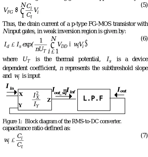
Fig. 1 shows the block diagram of the current-mode true RMS-to-DC converter that consists of two separate functions: a squarer/divider and a first order low pass filter. The operation of the squaring/division can be done by using an electrically simulated translinear loop, with the help of floating gate MOSFET transistors, and the averaging operation can be done by using a first order current-mode low-pass filter (lossy integrator).
3. FLOATING GATE MOSTRANSISTOR
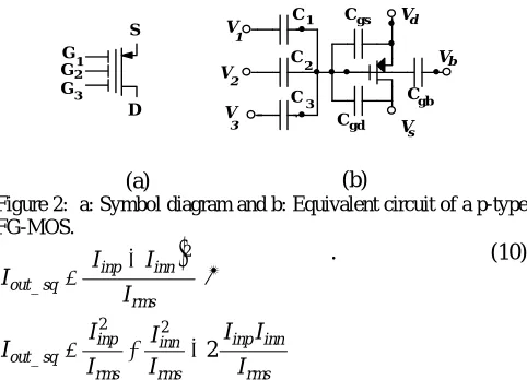
A floating gate MOS (FG-MOS) transistor with N input voltages V1,V2,...,VN consists of a floating gate electrode extended over the channel and N input gates located over the floating gate. In other words, the FG-MOS transistor is a MOS transistor with an isolated gate that capacitively coupled to the inputs. Fig. 2 shows the symbol diagram and equivalent circuit of a p-type FG-MOS transistor with 3 input voltages.
Applying charge conservation law, the voltage at the floating gate is given by:
∑
+ + + +=N
C Q V C C V C C V C C V C C V
t fg gb t gb gs t gs gd t gd i t i FG
1
(3 ) where Ci is the input capacitance between the floating gate and the i-th input, Ct is the total of these input capacitances, Cgd, Cgs, Cgb are the parasitic capacitors between the floating gate and the drain, source and bulk, respectively, and Qfg is residual charge trapped at the floating gate during fabrication process. This latter charge can be made negligible by using the technique described in [13]. If the sum of input capacitances is much larger than parasitic capacitances, i.e.,
gb gs gd N
i C ,C ,C C >>
∑ 1
(4)
then the voltage at floating gate can be approximated by:
∑
≅N V
C C
V i
t i FG
1
(5)
Thus, the drain current of a p-type FG-MOS transistor with
N input gates, in weak inversion region is given by:
(
)
∑
= −
= N
i
V w V nU ( exp I
I DD i i
T s
d
1
1 (6)
where UT is the thermal potential, Is is a device dependent coefficient, n represents the subthreshold slope and wi is input
out_sq=
L.P.F Y
X
Z
I
inf out
in I
I
I
Figure 1: Block diagram of the RMS-to-DC converter.
capacitance ratio defined as:
t i i
C C
w = (7)
4. SQUARER/DIVIDER AND LOW PASS FILTER CIRCUITS: ANALYSIS AND SYNTHESIS
A. Squarer/Divider Circuit
The squarer/divider can be implemented by using of sigma-delta data converter [3], MOS translinear [8], [12], [14] or class-AB tranconductance [7] circuits. Employing sigma-delta converter needs a large number of transistors, switches, and capacitors that leads to a high circuit complexity, chip area and power consumption [6]. MOS translinear circuits can be categorized as follows: stacked loop, up-down loop and electronically simulated loop [15]. The stacked loop [14] similar to class-AB tranconductance suffers from body effect. Influence of the body effect in up-down loop [8] is smaller than in stacked loop but more circuits for current injection in transistors are required. In the electronically simulated loop, the body effect is completely eliminated but a lot of additional circuitry is needed to force the two averages of the gate-source voltages of the loop be equal [12]. In addition, all these proposed squarer/divider circuits operate in only one quadrant input current. To make the input current of the squarer/divider operate in two-quadrant with positive and negative currents, a new synthesis by employing of FG-MOS transistors is presented. This will cause the squarer/divider to act as a full wave rectifier with large dynamic range and lower static power consumption. To this end, the input current
I
inis split into its differential representation (Iinp ,Iinn) whichY X
are both strictly positive and are related to Iin by:
inn inp
in I I
I = − (8)
Also the input-output relation of the squarer/divider block in current-mode is given by:
rms in sq _
out I /I
I = 2 (9)
where Iout_sq is the output of the block,Iinis the squared input of the block (which is also equal to the input of the converter as shown in Fig. 1) and Irms=Iout is the divisor input of the block (which is also equal to the output of the converter and the filter as shown in Fig. 1). Using (8) and (9), it is obtained that:
2 G3 V V 2 1 V V 3 d V s 3 2 1 gs 1 gd C C C C C C V G D S gb G b
Figure 2: a: Symbol diagram and b: Equivalent circuit of a p-type FG-MOS.
(
)
rms inn inp sq _ out I I I I 2 − =→
rms inn inp rms inn rms inp sq _ out I I I I I I I I 2 2 2 − + =. (10)
The right hand side (RHS) of (10) consists of three one-quadrant functions: two squarer/dividers and one multiplier. For implementation of these functions, the p-type FG-MOS transistors are employed. Fig. 3 shows the circuit of a one-quadrant squarer/divider consisting of three FG-MOSs, where it is assumed all transistors are operating in weak inversion region. The I-V relationships for transistors M1, M2 and M3 are given by:
(
)
(
)
⎟⎟ ⎠ ⎞ ⎜⎜ ⎝ ⎛ + −= 11 1 12 1
1 1 V w V w V nU exp I I DD T s (11)
(
)
(
)
⎟⎟ ⎠ ⎞ ⎜⎜ ⎝ ⎛ + −= 21 2 22 2
2 1 V w V w V nU exp I I DD T s (12)
(
)
(
)
⎟⎟ ⎠ ⎞ ⎜⎜ ⎝ ⎛ + −= 31 1 32 2
3 1 V w V w V nU exp I I DD T s (13)
Assuming that w11=w12=w21=w22=w31=w32=1/2,
squaring both sides of (13) and then substituting (11) and (12) into it, the following expression will be obtained:
2 1 2
3 I I
I =
→
2 2 3 1 I I
I = (14)
Therefore, a one-quadrant squarer/divider circuit is obtained
by taking a copy of I1 as the output, while I2andI3 are as
the inputs.
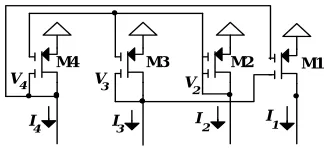
Fig. 4 shows the circuit of a one-quadrant multiplier which consists of four FG-MOSs that operate in weak inversion.
The I-V relationships for transistors M1, M2, M3 and M4 are given by:
(
)
(
)
⎟⎟ ⎠ ⎞ ⎜⎜ ⎝ ⎛ + −= 11 3 12 4
1 1 V w V w V nU exp I I DD T s (15)
(
)
(
)
⎟⎟ ⎠ ⎞ ⎜⎜ ⎝ ⎛ + −= 21 2 22 2
2 1 V w V w V nU exp I I DD T s (16)
(
)
(
)
⎟⎟ ⎠ ⎞ ⎜⎜ ⎝ ⎛ + −= 31 2 32 3
3 1 V w V w V nU exp I I DD T s (17)
(
)
(
)
⎟⎟ ⎠ ⎞ ⎜⎜ ⎝ ⎛ + −= 41 2 42 4
4 1 V w V w V nU exp I I DD T s (18)
By assumption that = = = = = =
= 12 21 22 31 32 41
11 w w w w w w
w
2 1 42 /
w = , from (15), (16), (17) and (18) it results:
M1 M2 M3 I 1 I 2 3 I V 1 V 2
Figure 3: A FG-MOS based one-quadrant squarer/divider.
4 3 2 1I I I
I =
→
2 4 3 1 I I I
I = . (19)
Therefore, a one-quadrant multiplier circuit is obtained by taking a copy of I1 as the output, and copies of I2 ,
3
I andI4 as the inputs.
The source and substrate of transistors of the two above mentioned circuits are connected to supply voltage so the effect of the body effect is completely eliminated. Also, the complexity of these two circuits is much lower than those of up-down and electronically simulated MOS translinear based circuits.
Fig. 5 shows the complete circuit of the proposed two-quadrant squarer/divider circuit which is implemented based on equations (8) and (10). Transistors M1, M4 and M5 and transistors M2, M4 and M6 of Fig. 5 form two one-quadrant squarer/dividers for implementation of the first and second terms of RHS of (10) according to Fig. 3. Transistors M3, M4, M5 and M6 form a one-quadrant multiplier. This multiplier and current mirror transistors (M9, M10) are employed for implementation of the third term of RHS of (10) according to Fig. 4. The common elements of these three circuits are merged. For implementation of (8)
transistors M5, M6, M7 and M8 are employed.
As Fig. 5 shows, the sources of FG-MOSs are connected to the substrate, so the body effect is completely eliminated. Also, the figure shows the minimum supply voltage of the circuit is one Vgsplus oneVds, and since extra biasing current and voltage are not needed, the static power consumption is decreased. Since the FG-MOSs operate in weak inversion region, the power consumption is very low and dynamic range is large.
It should be pointed out that the RMS-DC converters that are based on the sigma-delta modulators [6] operate in voltage- mode. But for being used in the systems that work in
I
1
I
2 3
I M4
4
I
4
V V
3 2
M1 V
M2 M3
Figure 4: A FG-MOS based one-quadrant multiplier.
X2
M9 M10
inp
I
inn
I
I
rms
M7 M8
M4 M3 M2 M1
out_sq in
I
M6 M5
I
Figure 5: Circuit diagram of the two-quadrant squarer/divider.
the voltage-mode, the proposed converter and other existing current-mode RMS-DC converters [7], [8] need additional circuits for voltage-to-current converter at the input and current-to-voltage converter at the output. Also, the maximum operating frequency of the proposed converter with the MOS transistors that operate in the weak inversion is less than the frequency of the converters with MOS transistors that operate in the strong inversion [6], [7], [8].
B. Low Pass Filter Circuit
The current-mode filter of the RMS-to-DC converter can be implemented by using of switched capacitor [6], MOS translinear [8]-[12] or class-AB transconductance [7] circuits. In this paper, a simplified current-mode filter based on a novel synthesis is proposed. In Laplace domain the
transfer function of the filter can be written as:
( )
( )
c
s 1
1
ω + =
s I
s I
inf
outf (20)
in whichωc is the cutoff frequency,Ioutf
( )
s is the output current andIinf( )
s is the input current of the filter. Equation (20) in time domain can be written as:(
inf outf)
c outf
I I dt
dI
− ω
= (21)
To implement the filter we use the circuit shown in Fig. 6 in which output current Ioutf
( )
t is nonlinearity related to a certain capacitor voltage Vcap( )
t by:⎟ ⎟ ⎠ ⎞ ⎜ ⎜ ⎝ ⎛ =
T nU
cap V exp I Ioutf S
(22)
Using equations (21) in (22) and also equation
dt dV C
Icap= cap result:
(
inf outf)
outf c T
cap I I
I C nU
I = ω − . (23)
As shown before in Fig. 1, the output current of the filterIoutf is equal to the output current of the RMS-to-DC converterIout, and the input current Iinf is equal to
out in/I
I2 . Applying these two substitutions to (23) gives:
⎟ ⎟ ⎠ ⎞ ⎜
⎜ ⎝ ⎛
−
= out
out in
out c T
cap I
I I I
C nU I
2
ω (24)
M1
C
I ou
tf
I
cap
V
ca
p
Figure 6: Current-mode SRD filter principle.
Considering the cutoff frequency of the filter as C
nU Iout T c = /
ω , equation (24) can be rewritten as
⎟ ⎟ ⎠ ⎞ ⎜
⎜ ⎝ ⎛
−
= out
out in
cap I
I I I
2 (25)
C gm c =
ω (26)
in which T outf out , gs out m nU I V I g = ∂ ∂
= is the linear
tranconductance of output transistor M1. Substituting gm
in (26) results:
C nU I C nU I T out T outf
c = =
ω (27)
Eqn. (27) shows that the condition of ωc considered on extraction of eqn. (25) is satisfied.
Comparing this filter with other proposed filters which are realized based on the switched capacitor technique [6] or is implemented by three translinear loops [8]-[12], or by two class-AB transconductors [7], shows that this analysis gives a much simpler circuit. To obtain this simple circuit, as equation ωc =Iout /nUTC indicates, the cutoff
frequency of the filter is allowed to vary with output current. This dependency toIout, and also the maximum
acceptable output ripple determine the suitable values for capacitor C. This subject is discussed next.
The output current of the RMS-to-DC converter is a DC currentItrue−RMS with an ac rippleIripple on it. In order that converter gives a good performance the amplitude of this ripple should be small compared toItrue−RMS. This requires suitable values for the cutoff frequency of the filter.
As it is mentioned above,ωc is proportional to the output current of the converter; however the value of the capacitor can be calculated in such a way that it eliminates the effect of this dependency and also achieves enough accuracy in the output of the converter. To this end, we first substitute
f , in
I andIout,f in (21) that results:
I inf I ou tf M1 C I I ou tf ca p Vcap
Figure 7: Circuit diagram of the proposed low pass filter.
⎟ ⎟ ⎠ ⎞ ⎜ ⎜ ⎝ ⎛ − ω = out out in c out I I I dt
dI 2 (28)
Multiplying both sides of eqn. (28) by Iout gives:
(
2 2)
out in c outout I I
dt dI
I =ω −
→
( )
(
2 2)
22 c in out out I I dt I d − ω =
. (29)
Eqn. (29) is time domain representation of a current-mode filter with input ofIin2, output of
2
out
I and cutoff frequency of2×ωc. In Laplace domain, the equation can be rewritten as:
( )
( )
c 2 2 2 s 1 1 ω + = s I s I in out (30)Assuming that the input current is a sinusoidal function we have:
) t cos( I
Iin = 2 true−RMS ω (31)
where ωis the frequency of the input current of the converter. Squaring both sides of eqn. (31) gives the input signal of (30) as follows:
) t ( cos I
Iin2 = 2 true2 −RMS 2 ω
→
(
)
(
cos t)
I
Iin2 = true2 −RMS 1+ 2ω
(32)
A low pass filtering method for solvingIout was presented in [16] and is adopted in our present analysis. Using input signal of eqn. (32) in low pass filter of eqn. (30) gives:
(
)
(
+ ω + φ)
= I − B cos t
Iout2 true2 RMS 1 2 (33)
where
(
)
22 2 1 1 c / B ω ω +
= and ⎟⎟
⎠ ⎞ ⎜ ⎜ ⎝ ⎛ ω ω − − = φ c tg 2 2
1 . (34)
Assuming that ωc <<ω and using Taylor series expansion gives:
(
)
(
+ ω +φ)
=I − Bcos t
Iout true RMS 1 2
(
)
(
)
⎟⎟ ⎠ ⎞ ⎜ ⎜ ⎝ ⎛ + φ + ω − φ + ω +≅Itrue−RMS Bcos t B cos 2 t "
8 2 2 1 2 2
(
)
(
)
⎟⎟ ⎠ ⎞ ⎜ ⎜ ⎝ ⎛ + φ + ω − φ + ω + −≅ − 4 2 "
8 2 2 16 1 2 2 t cos B t cos B B
Itrue RMS .
(35) From (35) RMS and peak-to-peak ripple values at the output current are expressed by:
RMS true out , RMS I B
I ⎟⎟ −
⎠ ⎞ ⎜ ⎜ ⎝ ⎛ − = 16 2
1
→
(
)
true RMS out,
RMS I
C / /
I ⎟⎟ −
⎠ ⎞ ⎜
⎜ ⎝ ⎛
ω ω + − =
2
2 2 1
16 1 1
RMS true out
,
ripple I
B
I = −
2
→
(
)
true RMSC out
,
ripple I
/ /
I −
ω ω + =
2
2 2 1
2 1
(36b)
From (36) it can be concluded that if the frequency of the input signal is at least five times bigger than the cutoff frequency of the filter
(
ω≥5ωc)
, then the accuracy of more than 1% can be obtained at the output.Assuming ωmin as the lower end of the frequency range andItrue−RMS,maxas the higher end of the RMS of the input (output) current range, using (26), and considering condition
(
ω≥5ωc)
results the values of the capacitor for achieving the accuracy of more than 1% as:min T
max , RMS true
nU I C
ω
≥ 5 − (37)
More accuracy at the output of the converter can be achieved by decreasing the cutoff frequency of the filter by employing larger capacitances or reducing linear tranconductance according to equation (26).
5. SECOND-ORDER EFFECTS
The expressions presented in the previous sections are valid by assumption that influences of the second-order effects that cause deviations from the ideal exponential-law behavior of MOS (or FG-MOS) transistors are negligible. The body effect is the change of the threshold voltage Vth
caused by the source-to-substrate bias of MOS transistors. As it has already been mentioned, due to the fact that the source of all transistors in the electronically simulated translinear loop is connected to the substrate, the body effect is completely eliminated.
The channel-length modulation causes the drain current to be dependent on the drain voltage and its dependency is inversely proportional to the channel lengthL. Long channel transistors have been employed in our proposed circuit, to eliminate this effect. These large lengths also reduce the mobility degradation effects and conductance of transistors.
Contribution of parasitic capacitorsCgd,Cgs Cgb in FG-MOSs has minor effect on the operation of converter by choosing the input capacitances much larger than the parasitic capacitors [17].
Fabrication tolerance and process gradients lead to mismatch between transistor parameters. The mismatch
between input capacitances of FG-MOS transistors is more important in squarer/divider block. The analytical effects of these mismatch is reported in [17] that demonstrates the increase of second and third harmonic distortion. If the converter uses a low-pass filter with cutoff frequency of much less than the input current frequency, the influence of mismatch is considerably reduced. This is shown in simulation results of mismatch effects in section 6.
6. SIMULATION RESULTS
The complete circuit diagram of the proposed RMS-to-DC converter is depicted in Fig. 8. The circuit was designed by LEDIT and then post layout simulation using HSPICE with TSMC 0.35um CMOS process parameters, with
V .
Vth,n ≅054 and Vth,p ≅− 0.65V. Vdd=0.9V and C=300nF were employed. The aspect ratio of the FG-MOS transistors (M1-M6) was chosen as 20um/10um and for the current-mirrors transistors (M7, M8, M9) and transistor (M10) the corresponding values were 10um/10um and 20um/10um respectively. For the output transistors (M11-M13) the aspect ratio was 60um/10um. Most SPICE simulators have convergence problems with floating nodes during the operating point calculations, so an N-input FG-MOS model presented in reference [18] is used for simulation. Fig. 9 shows the steady-state time response of the converter for a sinusoidal input current with 100nA peak-to-peak amplitude and 100 Hz frequency. Fig. 10 shows the output current relative error defined as:
Relative error=
(
)
(
)
(
)
* %l theoritica I
simulated I
l theoretica I
out
out out
100
−
(38)
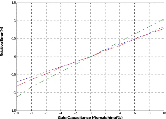
for different amplitudes of the sinusoidal input current. The figure reveals that errors less than 3% can be found for input current amplitudes from 0.3nA to 350nA. This input range with low supply voltage is much wider than those reported before [6]-[8]. Fig. 11 shows the simulation result of relative error in output current affected by mismatching in the input capacitance ratio of individual transistors M3, M5 and M6 for a sinusoidal input current with 100nA peak-to-peak amplitude and 100 Hz frequency. As Fig. 11 shows, even by deviation of the ratios from -10% to +10% the relative error less than
±
1.5% is resulted. It should be noted that deviation values of±
10% have been overestimated.Simulation results showed the power consumption of 1.5uW for the maximum accepted input current (350nA).
converters.
X2
M12
out
I
M13 M9
M10
M11
C
M7 M8
M4 M3 M2 M1
I
in
M6 M5
Figure 8: Complete circuit diagram of the RMS-to-DC converter
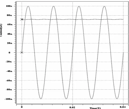
Figure 9: Time response of the input current (dotted) and output current (solid) of the RMS-to-DC converter.
100 101 102
-8 -6 -4 -2 0 2 4 6 8 10
Input current(nA)
Rel
a
ti
ve
E
rro
r(
%
)
-10 -8 -6 -4 -2 0 2 4 6 8 10 -1.5
-1 -0.5 0 0.5 1 1.5
Gate Capacitance Mismatching(% )
Rel
a
ti
v
e
Er
ro
r(
%
)
Figure 11: Relative error vs. mismatch input capacitances ratioof transistors M3 (dotted), M5 (dash-dot) and M6 (dashed).
TABLE 1
A COMPARISON BETWEEN RMS-TO-DC CONVERTERS.
Converter[8] Converter[7] Converter[6] This Work
Basic principle MOS up-down translinear
Class-AB tranconductance
Sigma-Delta data converter
FG-MOS transistors
Technology 2.4u 0.5u 0.8u 0.35u Minimum voltage Vgs +2Vds
(1.5V)
ds gs V V +2
(1.5V) ( ±3V )
ds gs V
V +
(0.9V) Circuit complexity
(Transistor number)
High (108 tr.)
Medium (40 tr.)
Very high (>>150)
Low (11)
Input current range 5uA-11uA @2%error
12uA-22uA @3%error
0.4V @2%error
0.7nA-350nA @3%error
Power consumption Not reported but
Expected >>100uW > 200uW 40mW
< 2uW @400nA Operation area of
Input current 1 quadrant 1 quadrant 1 quadrant 2 quadrant Influence of
the Body Effect Medium High Low Zero
Operation mode Current-mode Current-mode Voltage-mode Current-mode
7. CONCLUSIONS
A two-quadrant squarer/divider circuit that employs FG-MOS transistors operating in weak inversion region is presented. The circuit that operates in two-quadrant input current is immune from body effect, works at low voltage
8. References
[1] S.A.P.Haddad, S.Gieltjes, R.Houben, and W.A.Serdijn, "An ultra low-power dynamic translinear cardiac sense amplifier for pacemakers," in IEEE Int. Symp. Circuits Syst., ISCAS’03, vol. 5, pp. V-37-V-40, May 2003.
[2] Analog Devices, AD636 Data Sheet, "Low level True RMS-to-DC converter," Available: http://www.selectronic.fr/ includes_ selectronic/pdf/Analog_Device/AD636JH.pdf.
[3] N.Krishnapura, "Large dynamic range dynamically biased log-domain filters," PhD thesis, Columbia University, USA, 2000.
[4] J.Mulder, A.C.V.D.Woerd, W.A.Serdijn,and A.H.M.V. Roermund, "An RMS-DC converter based on the dynamic translinear principle," IEEE J. Solid-state circuits, vol. 32, no.7, pp. 1146-1150, Jul. 1997. [5] J.Mulder, W.A.Serdijn, A.C.V.D.Woerd, and A.H.M.V. Roermund,
"Dynamic translinear RMS-DC converter," Electron. Lett., vol. 32, no. 22, pp. 2067-2068, Oct. 1996.
[6] W.S.Wey, and Y.C.Huang, "A CMOS delta-sigma true RMS converter," IEEE J. Solid-state Circuits, vol. 35, no. 2, pp. 248-257, Feb. 2000.
[7] C.A.DE La Cruz-Blas, A.J.Lopez-Martin, A.Carlosena and J.Ramirex-angulo, "1.5v current-mode CMOS true RMS-DC converter based on class-AB transconductors," IEEE Trans. Circuits Syst. II, Express Briefs, vol. 52, no. 7, pp. 376-379, Jul. 2005. [8] A.J.Lopez-Martin, and A.Carlosena, "A 1.5V current-mode CMOS
RMS-to-DC converter," Analog Integrated Circuits Signal Process., vol. 36, pp. 137-143, 2003.
[9] M.Eskiyerli, and Payne, "Square root domain filter design and performance," Analog Integr. Circuits Signal Processing, vol. 22, pp. 231-243, 2000.
[10] J.Mulder, A.C.V.D.Woerd, W.A.Serdijn, and A.H.M.V. Roermund,
"Current-mode companding x−domain integrator," Electron. Lett. , vol. 32, no.3, pp.198-199, Feb. 1996.
[11] A.J.Lopez-Martin and A.Carlosena, "A 1.5v CMOS companding filter," Electron. Lett, vol. 38, no.22, pp. 1346-1348, 2002.
[12] C.Psychalinos and S.Vlassis, "A systematic design procedure for square-root -domain circuits based on the signal flow graph approach," IEEE Trans .Circuits Syst. I, Fundam. Theory Appl., vol. 49, no. 12, pp. 1702-1712, Dec. 2002.
[13] E.O.Rodriguez-villegas and H.Barnes, "solution to trapped charge in FGMOS transistors," Electron. Lett. , vol. 39, pp. 1416-1417, Sep. 2003.
[14] Bin-Da Liu,Chuen-Yau Chen , and Ju-Ying Tsao, "A modular current-mode classifier circuit for template matching application," IEEE. Trans. Circuits Syst. II, Analog Digit. Signal Process, vol. 47, no. 2, pp. 145-151, Feb. 2000.
[15] E.Seevinck and R.J.Wiegerink, "Generalized translinear circuit principle," IEEE J. Solid -State Circuits, vol. 26, no. 8, pp. 1098-1102, Aug. 1991.
[16] D.R.Frey, "Exact analysis of implicit RMS converters," Electron. Lett. , vol. 40, no. 5, pp. 1455-1456, March 2004.
[17] E. Rodriguez-Villegas, A.Yúfera, and A. Rueda, "A 1.25-V micropower Gm-C filter based on FGMOS transistors operating in weak inversion," IEEE J. Solid-State Circuits, vol. 39, no. 1, pp. 100-111, Jan. 2004.