warwick.ac.uk/lib-publications
Manuscript version: Author’s Accepted Manuscript
The version presented in WRAP is the author’s accepted manuscript and may differ from the
published version or Version of Record.
Persistent WRAP URL:
http://wrap.warwick.ac.uk/123466
How to cite:
Please refer to published version for the most recent bibliographic citation information.
If a published version is known of, the repository item page linked to above, will contain
details on accessing it.
Copyright and reuse:
The Warwick Research Archive Portal (WRAP) makes this work by researchers of the
University of Warwick available open access under the following conditions.
Copyright © and all moral rights to the version of the paper presented here belong to the
individual author(s) and/or other copyright owners. To the extent reasonable and
practicable the material made available in WRAP has been checked for eligibility before
being made available.
Copies of full items can be used for personal research or study, educational, or not-for-profit
purposes without prior permission or charge. Provided that the authors, title and full
bibliographic details are credited, a hyperlink and/or URL is given for the original metadata
page and the content is not changed in any way.
Publisher’s statement:
Please refer to the repository item page, publisher’s statement section, for further
information.
New Insights into the Thermally Activated Defects in n-type
Float-Zone Silicon
Yan Zhu
1, a)Fiacre Rougieux
1, Nicholas Grant
2, Jack Mullins
3, Joyce Ann De
Guzman
3, John D. Murphy
2, Vladimir P. Markevich
3, Gianluca Coletti
1, 4, Anthony
R. Peaker
3, and Ziv Hameiri
11University of New South Wales, Sydney, NSW 2033, Australia 2University of Warwick, Coventry, CV4 7AL, United Kingdom 3University of Manchester, Manchester, M13 9PL, United Kingdom
4ECN part of TNO, Le Petten, NL-1755, Netherlands
a)Corresponding author: [email protected]
Abstract. Float-zone silicon has been long assumed to be bulk defect free and stable. Nevertheless, recently it was found that upon annealing between 450 °C to 700 °C detrimental defects can be activated in this material. Previous studies via deep level transient spectroscopy have identified several defect levels. However, it is still not clear which of these levels have a substantial impact on the minority carrier lifetime. In this study, we determine the recombination parameters of the dominant defect level using a combination of deep level transient spectroscopy and temperature and injection dependent lifetime spectroscopy. Additionally, we investigated the effect of hydrogenation on the thermally activated defects in n -type float-zone silicon.
INTRODUCTION
Providing high minority carrier lifetime, float-zone (FZ) silicon has been long conceived as a bulk defect lean and stable material. Therefore it is widely used in the photovoltaic community for the fabrication of high efficiency solar cells,1,2 control wafers of various experiments,3,4 monitoring surface passivation quality,5,6 modeling intrinsic
recombination7etc. Nevertheless, recently it was found the lifetime of FZ silicon can drop by more than two orders
of magnitude after a heat treatment between 450 to 700 °C. 8,9 This severe degradation was found to be due to the
activation of bulk defects during the heat treatment.8,9 Therefore, special care is needed if the FZ silicon wafers used
undergo processes in the temperature range between 450 to 700 °C. Fortunately, it was found that the thermally activated defects can be permanently deactivated after an annealing at 1000 °C for 30 mins.8,9 It was suspected that
the defects activated during the degradation are related to the nitrogen doping during crystal growth and un-clustered vacancies.10 More recent studies reveal that FZ wafers can also degrade under light and elevated temperature.11,12
Deep level transient spectroscopy (DLTS) measurements from previous studies have found several defect levels in the degraded samples.8,10 However, DLTS alone does not reveal which level is the dominant in the recombination
of charge carriers. Temperature and injection dependent lifetime spectroscopy (TIDLS) is another technique widely used for defect characterization.13,14 As it is based on lifetime measurements on bulk samples, TIDLS is more
sensitive to the dominant defect levels which limit the effective lifetime of the sample. The purpose of this study is to determine the dominant recombination level in annealed FZ silicon wafers by combining TIDLS and DLTS, and to explore the effect of hydrogenation passivation on the thermally activated defects. In this work, we focus only on
METHODS
Three groups of 4 inch diameter n-type FZ silicon wafers (1 Ωcm, grown in a nitrogen ambient) from the same manufacturer were prepared. Group N (no anneal) contains three as-grown wafers without any thermal process. Group D (degraded) contains four wafers annealed at 500 °C under nitrogen ambient for 30 mins. Group A (defect annihilated) contains three wafers annealed at 1000 °C under nitrogen ambient for 30 mins. Since the wafers may not be neighboring wafers from the same ingot, multiple wafers are used in each group to improve the statistics of the measurements.
After annealing, room temperature lifetime and photoluminescence (PL) imaging of all wafers were firstly measured by means of superacid-derived passivation [bis(trifluoromethane)sulfonimide (TFSI) in 1, 2-dichloroethane (DCE)].15 Superacid-derived passivation provides excellent passivation quality (surface
recombination velocity, SRV, around 1 cm/s) and does not add thermal budget to the samples (as it is conducted at room temperature).15 After room temperature measurements with superacid-derived passivation, the samples then
went through RCA cleaning and an amorphous silicon (a-Si) surface passivation via plasma-enhanced chemical vapor deposition (PECVD). To minimize the thermal budget on the samples, the deposition temperatures were kept below 200 °C. This a-Si layer was found to provide a stable passivation up to 200 °C with an SRV below 10 cm/s. TIDLS measurements were then performed from -50 to 150 °C using a customized quasi-steady-state photoconductance lifetime tester based on the WCT-120 from Sinton Instruments.16 A cryostat has been
incorporated into the system to enable lifetime measurements at various temperatures.
After TIDLS measurement, the a-Si layer was stripped off from the samples (a mixture of 49% hydrofluoric acid and 69% nitric acid with a ratio of 1:10 for two minutes followed by rinsing in deionized water). DLTS measurements were then performed on one wafer from each group. Schottky barrier diodes were fabricated by thermal evaporation of gold (Au) to the front surface of the samples, while ohmic contacts were fabricated by thermal evaporation of aluminum (Al) to the back surface. In order to investigate the effect of hydrogenation of the thermally-activated defects, another wafer from each group went through a silicon nitride (SiNx) surface
re-passivation via PECVD.17 The temperature of the deposition was around 425 °C. No additional firing has been done
to the samples after the SiNx deposition.
RESULTS
Thermal Activation of the Defects
[image:3.612.82.509.437.627.2](a) (b)
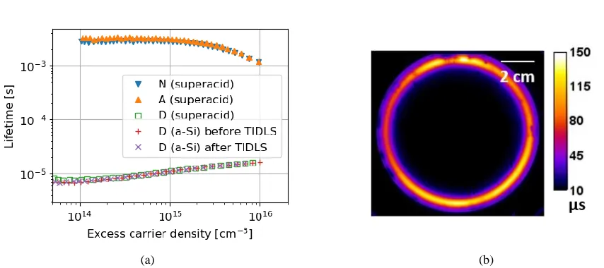
FIGURE 1. (a) Room temperature injection dependent lifetime curves of the 1 Ωcm n-type FZ-Si samples with
Room temperature injection dependent lifetime curves of the samples from each group after the superacid-derived passivation are shown in Fig. 1 (a). As can be seen, the lifetime of the degraded sample (Group D) is two orders of magnitude lower than the as grown sample (Group N) and the defect-annihilated sample (Group A) across the entire measured injection range. This indicates the effective lifetime of the degraded sample is dominated by the recombination lifetime of the activated bulk defects.
The room temperature photoluminescence (PL) image of the degraded sample after the superacid-derived passivation is shown in Fig. 1(b). The PL counts at the center of the wafer is much lower than the PL counts at the periphery, indicating that the activated defects have a non-uniform spatial distribution. This characteristic agrees with previous studies of these thermally activated defects in FZ silicon.8,9 In this study, the lifetime curves and
DLTS spectra of the degraded samples are all measured from the center.
The room temperature lifetime curves of the degraded sample with a-Si passivation before and after the TIDLS measurements are also shown in Fig. 1(a). These two lifetime curves are similar to the lifetime curve of the degraded sample with a superacid-derived passivation, indicating (a) the a-Si layer provides surface passivation quality that is sufficient for the effective lifetime of the degraded sample to be dominated by the activated bulk defects; (b) the thermally activated defects were not impacted by the deposition process of the a-Si layer; and (c) the thermally activated defects were not impacted by the TIDLS measurements.
Electrical Characterization of the Defects
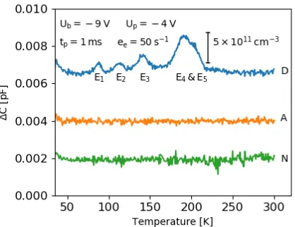
The electrical properties of the thermally activated defects are investigated by a combination of DLTS and TIDLS. The measured DLTS spectra are shown in Fig. 2. No clear electron emission signals are detected in the spectra of the as-grown sample (Group N) or the defect-annihilated (Group A) sample. In the DLTS spectrum of the degraded sample (Group D), four distinguished peaks can be observed. With a Laplace-DLTS analysis,10 it was
found that the peak at around 180 K consists of contributions from two electron emission signals. The activation energies for electron emission from the observed traps, E1-E5, have been determined as 0.16±0.005, 0.20±0.005,
0.28±0.005, 0.405±0.01 and 0.43±0.01 eV, respectively. These defect levels are similar to the ones identified by Grant et al.8 In the degraded samples studied by Grant et al.8, the E
3 center had the highest concentration among all
the traps, whereas according to our results the E4 and E5 traps have higher concentrations. In either case, it is unclear
which level is most responsible for the dramatic decrease of lifetime.
By changing the filling pulse length in the DLTS measurements, it was found that the electron capture cross sections σn of the E1, E2, E3 and E4 traps are larger than 10-16 cm2 with weak (if any) temperature dependence,
whereas σn of the E5 trap shows an exponential growth with temperature according to the following equation, σn = 7×10⁻¹⁶exp(−0.19/kT) cm2. Minority carrier transient spectroscopy (MCTS) measurements were also performed;
[image:4.612.210.419.482.643.2]yet, no hole emission signal from a defect level in the lower half of the bandgap was observed.
FIGURE 2. DLTS spectra of one sample from each group. The spectra are shifted for clarity. The measurement settings are shown in the graph. Ub and Up are the reverse bias voltage and filling pulse voltage respectively, tp is the filling pulse length and
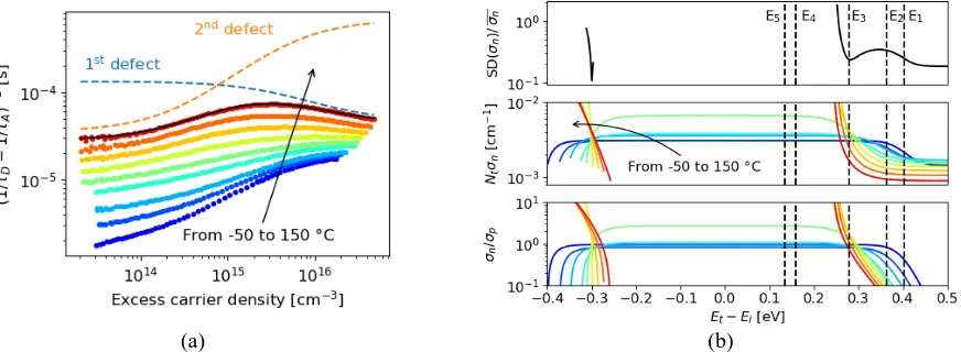
In order to quantify the recombination activity of the activated defects, TIDLS measurements were performed on the as-grown, degraded and annealed samples. For all temperatures, the lifetimes of control samples and defect-annihilated samples are nearly two orders of magnitude higher than the lifetimes of the degraded samples. Therefore, the impact of surface recombination and intrinsic recombination on the effective lifetime of the degraded samples can be considered as negligible. In our TIDLS analysis, we still use the inversely subtracted lifetime (1/τD−1/τA)−1 to further minimize the impact of surface and intrinsic recombination, where τD and τA are the lifetime of the degraded sample and defect-annihilated sample respectively. In Fig. 3(a), the inversely subtracted lifetimes of the degraded sample are shown for different temperatures.
[image:5.612.82.518.178.338.2](a) (b)
FIGURE 3. (a) Inversely subtracted lifetime (1/τD−1/τA)−1 from −50 °C to 150 °C, as well as a two defects fitting of the lifetime at 150 °C. (b) DPSS curves resulted from the TIDLS measurements.
The inversely subtracted lifetimes are then fitted with Shockley-Read-Hall statistics18,19 using the method
described in Murphy et al.20 and Morishige and Jensen et al.21 It was found that at least two defect levels are
required to achieve a satisfactory fitting of the measured data. In Fig. 3(a), the fitting of the lifetime at 150 °C is shown. At each temperature, the best fitted lifetime curve can be reproduced by infinite combinations of defect parameters (energy level Et and the productions of defect density Nt and the two capture cross sections σn and σp). These infinite combinations can be represented by the so-called defect parameter solution surface (DPSS) curve.13
Since for most of the measured temperatures, the 2st defect dominates the lifetime only at a narrow injection range,
the uncertainty of analyzing the 2nd defect can be large. Hence, here we focus only on the analysis of the 1st defect.
The DPSS curves for the 1st defect at each temperature are shown in the bottom two graphs of Fig. 3(b). Each curve
in these two graphs represents the infinite combinations of the Et, Nt·σn and σn/σp that can best fit the lifetime curve at that temperature. If it is assumed that σn is temperature independent, then all the DPSS curves for Nt·σn (middle figure) should intersect at the true Et of the defect. In the upper graph of Fig. 3(b), the standard deviation of σn normalized by their mean value is plotted. The black dashed lines in Fig. 3(b) represent the five defect levels identified by DLTS. As can be seen, the level E3 (0.28±0.005 eV) coincides with a local minimum in the standard
deviation curve. Since σn of E3 was found to be temperature independent by DLTS, this indicates that E3 is likely to
be the most dominating defect level at room temperature. From the DPSS curve for σn/σp (the bottom subfigure), the capture cross section ratio of this defect level at room temperature is around 0.88±0.09. Meanwhile, another local minimum of the standard deviation curve can be identified in the lower half of the bandgap. However, this defect level has not been detected by MCTS measurements.
Hydrogenation of the Activated Defects
The room temperature lifetime curves of a degraded sample (Group D) and a defect-annihilated sample (Group A) are shown in Fig. 4. The lifetime of the degraded sample with a-Si passivation is also shown for comparison. As can be seen, after SiNx deposition, the lifetime of the degraded sample has increased by one order of magnitude.
Since the effective lifetime of the degraded sample with a-Si passivation is dominated by the thermally activated bulk defects, this increase of lifetime indicates that some of the activated defects has been passivated during the SiNx
activated. Therefore, the passivation is not likely to be a result of a thermal effect. Instead, this passivation is likely resulted from the hydrogenation effect induced during the PECVD process. Similar results have also been found by Rougieux et al.22
After SiNx passivation, the lifetime of the degraded sample is still much lower than the lifetime of the
defect-annihilated sample, indicating that the hydrogenation occur in the PECVD process cannot fully passivate the activated bulk defects. Therefore, even if the n-type FZ silicon will be passivated by hydrogen rich SiNx film, the
[image:6.612.207.416.173.330.2]impact of the thermally activated defects still needs to be considered if the sample needs to be annealed in the temperature range leads to degradation.
FIGURE 4. Room temperature lifetime curves for a defect-annihilated sample (“A”) and a degraded sample (“D”) passivated with SiNx as well as the lifetime of the degraded sample passivated with a-Si.
CONCLUSIONS
FZ silicon should not be intuitively considered as bulk defect free or stable material. Annealing at 500 °C results in the formation of recombination active defects in n-type FZ silicon. These thermally activated defects can decrease the lifetime of the sample by more than two orders of magnitude. Using a combination of DLTS and TIDLS, we identified that the most recombination active defect level among the thermally activated defect levels is located at 0.28±0.005 eV below the conduction band, with a capture cross section ratio of 0.88±0.09 at room temperature. The effect of hydrogenation on the thermally activated defect is investigated by depositing a hydrogen rich SiNx film on
the degraded sample. It has been found that the thermally activated defects can be partially passivated solely from the hydrogenation occurring during the deposition (no additional firing).
ACKNOWLEDGMENTS
This work was supported by the Australian Government through the Australian Renewable Energy Agency under grant ARENA 2017/RND001. The views expressed herein are not necessarily the views of the Australian Government, and the Australian Government does not accept responsibility for any information or advice contained herein. Work at Warwick and Manchester was supported by the EPSRC SuperSilicon PV project (EP/M024911/1).
REFERENCES
1. J. Zhao, A. Wang, M.A. Green, and F. Ferrazza, Appl. Phys. Lett. 73, 1991 (1998).
2. A. Richter, J. Benick, F. Feldmann, A. Fell, M. Hermle, and S.W. Glunz, Sol. Energy Mater. Sol. Cells 173, 96 (2017).
3. M.A. Jensen, A. Zuschlag, S. Wieghold, D. Skorka, A.E. Morishige, G. Hahn, and T. Buonassisi, J. Appl. Phys. 124, 085701 (2018).
6. B. Hoex, S.B.S. Heil, E. Langereis, M.C.M. van de Sanden, and W.M.M. Kessels, Appl. Phys. Lett. 89, 042112 (2006).
7. A. Richter, S.W. Glunz, F. Werner, J. Schmidt, and A. Cuevas, Phys. Rev. B 86, 165202 (2012).
8. N.E. Grant, V.P. Markevich, J. Mullins, A.R. Peaker, F. Rougieux, and D. Macdonald, Phys. Status Solidi - Rapid Res. Lett. 10, 443 (2016).
9. N.E. Grant, V.P. Markevich, J. Mullins, A.R. Peaker, F. Rougieux, D. Macdonald, and J.D. Murphy, Phys. Status Solidi 213, 2844 (2016).
10. J. Mullins, V.P. Markevich, M. Vaqueiro-Contreras, N.E. Grant, L. Jensen, J. Jabłoński, J.D. Murphy, M.P. Halsall, and A.R. Peaker, J. Appl. Phys. 124, 035701 (2018).
11. D. Sperber, A. Herguth, and G. Hahn, Phys. Status Solidi - Rapid Res. Lett. 11, 1600408 (2017).
12. T. Niewelt, M. Selinger, N.E. Grant, W. Kwapil, J.D. Murphy, and M.C. Schubert, J. Appl. Phys. 121, 185702 (2017).
13. S. Rein, Lifetime Spectroscopy: A Method of Defect Characterization in Silicon for Photovoltaic Applications
(Springer Science and Business Media, Berlin, 2006).
14. S. Bernardini, T.U. Norland, G. Coletti, L. Ding, A.L. Blum, and M.I. Bertoni, in 43rd IEEE Photovolt. Spec. Conf. (IEEE, 2016), pp. 2863–2867.
15. N.E. Grant, T. Niewelt, N.R. Wilson, E.C. Wheeler-Jones, J. Bullock, M. Al-Amin, M.C. Schubert, A.C. Van Veen, A. Javey, and J.D. Murphy, IEEE J. Photovoltaics 7, 1574 (2017).
16. R.A. Sinton, A. Cuevas, and M. Stuckings, in 25th IEEE Photovolt. Spec. Conf. (IEEE, 1996), pp. 457–460. 17. Z. Hameiri, N. Borojevic, L. Mai, N. Nandakumar, K. Kim, and S. Winderbaum, IEEE J. Photovoltaics 7, 996
(2017).
18. W. Shockley and W.T. Read, Phys. Rev. 87, 835 (1952). 19. R.N. Hall, Phys. Rev. 87, 387 (1952).
20. J.D. Murphy, K. Bothe, R. Krain, V. V Voronkov, and R.J. Falster, J. Appl. Phys. 111, 113709 (2012).
21. A.E. Morishige, M.A. Jensen, D.B. Needleman, K. Nakayashiki, J. Hofstetter, T.A. Li, and T. Buonassisi, IEEE J. Photovoltaics 6, 1466 (2016).