Plasma and Fusion Research: Regular Articles Volume 14, 3402049 (2019)
Characterization of He Induced Nanostructures
Using SEM Image Analysis
∗
)
Hirohiko TANAKA, Shin KAJITA
1)and Noriyasu OHNO
Graduate School of Engineering, Nagoya University, Chikusa-ku, Nagoya 464-8603, Japan
1)Institute of Materials and Systems for Sustainability, Nagoya University, Chikusa-ku, Nagoya 464-8603, Japan
(Received 26 December 2018/Accepted 3 February 2019)
Helium induced nanostructures on tungsten were characterized by applying basic statistical analysis tech-niques to scanning electron microscope (SEM) images. As the analysis targets, pinhole- and fuzz-dominant surfaces irradiated with different ion fluences were employed. Although two-dimensional Fourier analysis of the normalized brightness of SEM images clarified several characteristic features, their differences are small to dis-tinguish the dominant nanostructures. On the other hand, probability density functions (PDFs) of the normalized brightness indicate that hole- and fuzz-dominant surfaces have long tail and Gaussian-like shape, respectively. By using several indexes with considering the black and white saturation, it was found that kurtosis and Kullback-Leibler divergence could provide reasonable judgement as the characterization index.
c
2019 The Japan Society of Plasma Science and Nuclear Fusion Research
Keywords: image analysis, statistical analysis, SEM, two-dimensional fast Fourier transform, probability density function, kurtosis, Kullback-Leibler divergence, pinhole, fuzz
DOI: 10.1585/pfr.14.3402049
1. Introduction
Tungsten (W) is thought to be the most promising ma-terial for the divertor target that should be irradiated with the high heat and particle fluxes in future magnetic fusion devices. From past researches, although W has quite low sputtering rate, helium (He) plasma irradiation could pro-voke several kinds of surface modifications such as bub-bles, pinholes, and fiberform nanostructures called fuzz, even if the incident ion energy was much smaller than the sputtering threshold [1]. Up to now, the fuzz-formation condition was deeply investigated and was found to be strongly related to the incident ion energy, surface tem-perature, and ion fluence [2]. Fuzzy nanostructure changes several surface physical characteristics, e.g., high light ab-sorptivity [3] and large surface area [4] due to an increase of the porosity [5]. Further, similar nanostructures are also found to be formed on other metals such as iron [6], vana-dium [7], platinum, and so on [8–10]. In order to utilize the unique characteristics of the fuzzy surface for an industrial application field, morphology-change conditions of several metals are energetically being surveyed.
The novel growth process of fuzzy structure has been attracted attention from modeling perspective. Density functional theory (DFT) and molecular dynamics (MD) were used for the nucleation of He clusters and bubbles and dislocation formation [11–14], and morphology changes were demonstrated using multi-scale simulations by the
author’s e-mail: [email protected]
∗)This article is based on the presentation at the 27th International Toki
Conference (ITC27) & the 13th Asia Pacific Plasma Theory Conference (APPTC2018).
combination of MD and Monte Carlo (MC) simulations [15, 16]. Even though those simulations still have a chal-lenging issue that they can only deal with a limited time and space, formations of initial protrusion and short fine structures were demonstrated.
To bridge the experiments and simulation, it is neces-sary to compare the grown structure quantitatively; frac-tal analysis has been conducted using scanning tron microscope (SEM) micrographs, transmission elec-tron microscope (TEM) micrographs, and gas adsorption isotherms [17–19]. It was found that initially formed pin-holes have a fractal feature in the size-number relation and the fuzzy structure has a multi-fractal feature. It is of inter-ests to further develop method to extract the specific char-acteristics of fuzzy structures grown by He plasma irradia-tion.
In this study, we applied basic statistical analysis tech-niques based on two-dimensional (2D) fast Fourier trans-form (FFT) and probability density function (PDF) to SEM images. As the He ion fluence increases, the fuzzy surface was formed with accompanying changes of several statisti-cal features. By introducing characterizing statistics and a measuring scale of PDFs, pinhole- and fuzz-dominant im-ages were distinguished. Such techniques are easy to ap-ply. Thus, these techniques could be easily shared among researchers and would be utilized for the parameter survey from a number of samples.
In Sec. 2, analyzed SEM images will be explained. Then, these images will be analyzed in Sec. 3. Finally, this study will be summarized in Sec. 4.
c
2019 The Japan Society of Plasma
Fig. 1 Analyzed SEM images of W samples: (a) W1, (b) W2, and (c) W3. Insets show magnified figures with the color scale fromμ−1.5σtoμ+1.5σ.
2. Analyzed SEM Images
We analyzed three W samples irradiated with He plasmas at different fluences in the linear plasma device NAGDIS-II [19]. Figure 1 shows the analyzed SEM im-ages: W1, W2, and W3, which are viewed from the normal direction to the surface. The He ion fluences of W1, W2, and W3 are 6×1024, 1.8×1025, and 4.7×1025m−2,
re-spectively. Sample information and irradiation conditions are summarized in Table 1 of Ref. [19]. On W1 surface, a number of pinholes can be found. As increasing the flu-ence, thicker convex structures appear in addition to pin-holes (see Fig. 1 (b)), and then, fuzzy nanostructure covers the surface (see Fig. 1 (c)).
Brightness (I) of these images is 8-bit grayscale which has 256 tonal steps fromI=0 (black) to 255 (white). The analyzed size of each image is 1080 pixels in vertical di-rection and 1600 pixels in horizontal didi-rection.
3. Image Analyses
As the basic technique for the image analysis, 2D FFT and PDF analyses were applied. For analyzing SEM im-ages, it should be taken into account that the mean of the
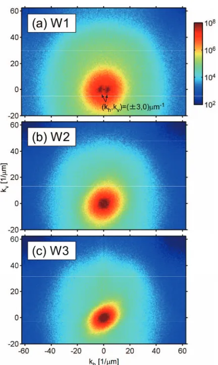
Fig. 2 2D power spectra ofInof (a) W1, (b) W2, and (c) W3 alongkhandkv.
brightness and the contrast can be changed depending on SEM devices, and beam and detector settings. Further-more, saturations in the brightness can occur depending on the settings.
In this study, to minimize the effects, the normalized brightness,In ≡(I−μ)/σ, was used for the analyses, where
μandσare the mean and the standard deviation of I in all pixels, respectively. Effects from the black and white saturation for 2D FFT and PDF analyses will be discussed later. Insets in Fig. 1 are magnified images with the color scale fromμ−1.5σtoμ+1.5σ. Their characteristic features associated with the analyses will be discussed in Sec. 3.1.
3.1
2D FFT
2D FFT analysis is widely used for identifying the crystalline nature particularly on TEM images [20, 21]. We investigated whether the 2D FFT analysis could find a dominant nanostructure from SEM images.
Figures 2 (a, b, c) shows 2D power spectra of In of
Plasma and Fusion Research: Regular Articles Volume 14, 3402049 (2019) respectively. Because a 2D power spectrum has a point
symmetric profile, kv<−20µm−1 range is not displayed
in Figs. 2 (a, b, c).
At around (kh,kv)∼(±3, 0)µm−1 in Fig. 2 (a), there
are unemphatic small peaks, indicating that there is a vertical-stripe component with a characteristic length of ∼1/3µm. Actually, in the inset in Fig. 1 (a), concavo-convex structures seem to be elongated not in the horizon-tal direction but in the vertical direction. This would reflect a stripe formation on single crystal W surfaces in the initial phase of He plasma irradiation [22]. In addition, profile of the 2D power spectrum of W3 seems to be slightly elon-gated to thekhkv>0 direction, implying that characteristic
length in the right oblique direction is slightly shorter than that in the left oblique direction. However, in any case, the spectral shape roughly looks like a concentric pattern.
Figure 3 (a) is azimuthally averaged power spectra of Figs. 2 (a, b, c) alongk=(k2
h+k 2
v)1/2. A little convex of
W1 at k ∼3µm−1 is attributed to the above-mentioned
vertical-stripe structures. A shoulder of W1 exists at
k ∼10µm−1 =(0.1µm)−1, and the wave number corre-sponds to the inverse of the typical diameter of pinholes (∼0.1µm) shown in the inset in Fig. 1 (a). Such shoul-der is observed when similar-size structures are nonperi-odically distributed [23]. Thus, it is found that pinholes are distributed nonperiodically. The power spectra of W3 has large component at smallerkrange, indicating that the fuzz forms a larger-scale rough surface compared with the typical size of pinholes on W1. Actually, submicrometer structures can be found in the inset in Fig. 1 (c). These larger-scale structures have no periodicity, because there is no spectral peak. The power spectrum of W2 looks like an intermediate between power spectra of W1 and W2. This
Fig. 3 Azimuthally averaged power spectra of (a)Inand (b) ar-tificially saturated and then normalizedInof W1 (solid), W2 (dashed), and W3 (dotted) alongk.
would be caused by the coexistence of pinholes and initial structures of fuzz.
In order to investigate the effect from the black and white saturation for these power spectra, artificially sat-urated images were analyzed. In this calculation, pixels withIless thanμ−1.5σand over thanμ+1.5σwere re-placed with−1.5σand 1.5σvalues, respectively. These ar-tificially saturated images, which correspond to the insets in Fig. 1, were normalized again and then analyzed with the 2D FFT. Figure 3 (b) shows the power spectra of the artificially saturated images. There is no clear difference between Fig. 3 (a) and Fig. 3 (b), indicating that a certain level of the black and white saturation is not a problem for the 2D FFT analysis.
From the analysis results, we found several character-istic features in three samples. However, because pinholes and fuzz have no periodicity, it is not easy to distinguish these structures from 2D FFT analysis.
3.2
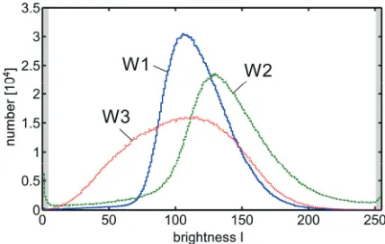
Next, we applied the PDF analysis. Figure 4 shows histograms of brightness I of three samples. They have peaks near the middle of the 256 tonal steps. Histograms of W1 and W3 become quite small at both ends. On the other hand, the histogram of W2 has small peaks atI=0 and 255, being attributable to the black and white saturation. Because the edge peaks largely affect the below-mentioned PDF analysis result in contrast to the power spectra, both ends of all histograms (∼2% in each end) were removed before the following analysis.
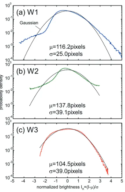
Figure 5 is semilogarithmic plots of PDFs as a func-tion ofIn. Integration of each PDF is equal to unity. PDF
tails are located within the range of−5≤In≤5 except for
a tail with a small amplitude in positiveInregion of W1. In
each figure, the standard Gaussian distribution (μ=0 and σ=1) is overplotted as a reference.
We can find significant differences between Figs. 5 (a, b) and Fig. 5 (c). The PDFs of W1 and W2 have tails in the negativeInregion with large amplitudes due to the
ex-istence of pinholes, which have darker colors (In<0). The
Fig. 5 PDFs of (a) W1, (b) W2, and (c) W3 as a function of the normalized brightness. Black dashed lines indicate the standard Gaussian distribution.
PDFs of W1 and W2 in the positiveIn region have also
larger amplitudes compared with the Gaussian distribution. This is mainly caused by brighter regions from the edge of pinholes and convex structures, because SEM image has higher brightness at the edge of structures due to secondary electron emissions from the edge face. In contrast, the PDF of W3 has no long tail and resembles the Gaussian shape due to the complicated fuzzy nanostructures. From Fig. 5, it is suggested that pinholes and fuzz could be dis-tinguished by comparing the PDF with the Gaussian distri-bution.
For characterizing a PDF, skewness (S) and kurtosis (K) are convenient indexes and often used in edge plasma field [24]. They are defined by
S ≡
(I−μ)3 σ3 =
In3
, (1)
K≡
(I−μ)4
σ4 −3=
In4
−3, (2)
where means an average. Since the Gaussian distri-bution has S =K=0, S and K values are utilizable for comparison with the Gaussian. If a PDF had a large am-plitude at positive/negativeIn tail region,S became
posi-tive/negative. Thus, the sign is important for S. On the
Fig. 6 (a) Skewness and (b) kurtosis of W1 (solid), W2 (dashed), and W3 (dotted) as a function ofIns.
other hand, positive and/or negative longer tail compared with the Gaussian producesK>0. Shorter tails in positive and negative directions makeKnegative.
Because the tail components are important forS and
K calculations, the effect from the black and white satu-ration should be taken into account. In order to confirm whether these statistics could be utilized quasi-universally for SEM images, sensitivities ofS andKagainst the satu-ration were investigated by artificially limiting theInrange.
In the following, signals satisfying|In|>Inswere removed
and a normalized brightness was then recomputed before theS andKestimations by introducing a saturation mag-nitudeIns.
Figure 6 shows the skewness and kurtosis as a func-tion ofIns. AtIns =5, where almost all data was used,S of
W1 is the largest in the three samples (see Fig. 6 (a)). As changingIns,S of W1 maintains the largest, while sign of
S switches on W2 and W3 samples. Considering the sen-sitivities ofS-sign onIns, discrimination of surface
nanos-tructures seems to be difficult fromS. On the other hand,
Kof W1 and W2 are larger than that of W3 for allInscases.
Furthermore, except for smallInscases,Kof W1 and W2
are positive and that of W3 is negative. This is caused by existence/nonexistence of the PDF tail. Therefore, Kis a possible candidate for the characterization index.
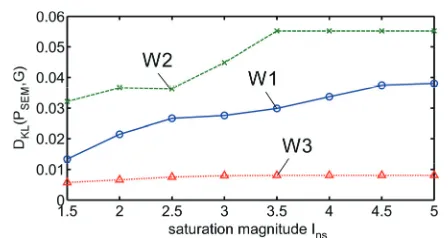
As a different candidate, Kullback-Leibler divergence (KLD) [25] is considered to compare the PDF with the Gaussian. The KLD is a famous scale for measuring dif-ference between two PDFs in probability and information theory fields and is also called “information divergence” and “relative entropy”. In plasma field, KLD was applied to turbulent signals [26]. The KLD (DKL) of a PDF (P)
against a different PDF (Q) distributing on the In axis is
Plasma and Fusion Research: Regular Articles Volume 14, 3402049 (2019)
Fig. 7 DKL(PSEM,G) of W1 (solid), W2 (dashed), and W3 (dot-ted) as a function ofIns.
DKL(P,Q)≡
∞
−∞P(In) log
P(In)
Q(In)
dIn. (3)
The DKL value is nonnegative, and DKL becomes zero
when Pand Qare the same. Although the KLD is also called “KL distance”, this is not a distance function, be-causeDKL(P,Q)DKL(Q,P).
In order to compare between a PDF from a SEM image (PSEM) and the Gaussian (G), DKL(PSEM,G) and
DKL(G,PSEM) can be calculated. Ideally, integration range
in Eq. (3) is from−∞to∞. However, far-edge tails are not acquired in a PDF from a SEM image due to the limited tonal range. BecausePlog(P/Q)=0 and∞when P=0 andQ=0, respectively, DKL(PSEM,G) has a finite value
andDKL(G,PSEM) becomes infinity if the integration range
contains aPSEM=0 region. Therefore,DKL(PSEM,G) was
only calculated as a function ofIns, as shown in Fig. 7.
Be-fore theDKLcalculation, signals satisfying|In|>Inswere
removed, and then the integral of thePSEMwas calibrated
to be unity. In allInsrange,DKL(PSEM,G) of W3 is much
smaller than those of W1 and W2. Thus, DKL(PSEM,G)
could be used for distinguish SEM images.
4. Summary
In order to characterize He induced nanostructures, we applied two basic analysis techniques to SEM images: 2D power spectrum and probability density function. To mini-mize the effects from the differences in contrast and bright-ness levels of SEM images, the normalized brightbright-ness was analyzed with taking into account of the black and white saturation.
From the 2D power spectra, nondirectional and non-periodic features of pinholes and fuzz are found. Because differences of these spectra are not significant, this method would be inadequate for distinguishing pinhole- and fuzz-dominant structures with the non-periodic nature.
In contrast, probability-density-function shapes calcu-lated from the brightness have a significant difference be-tween pinhole- and fuzz-dominant surfaces. The former surface has long tails in the PDF, while latter surface has a Gaussian-like shape. As a result, positive and negative kurtosis are observed in pinhole- and fuzz-dominant
im-ages, respectively, as if a certain level of brightness is sat-urated. Further, Kullback-Leibler divergence clearly indi-cates a resemblance with the Gaussian. In order to distin-guish pinhole- and fuzz-dominant SEM images, the kurto-sis and the Kullback-Leibler divergence would be useful.
For future work, it is of interests to apply the above-mentioned techniques to a number of SEM images with various nanostructures. Application of such characteriza-tion indexes would make it easy for researchers to survey parameter dependences. Further, above techniques could be applied to surfaces made in a computer simulation.
Acknowledgements
This research was supported by JSPS KAKENHI (16H06139), a grant from the Hibi Science Foundation, and the NINS program of Promoting Research by Net-working among Institutions (01411702).
[1] S. Takamura, N. Ohno, D. Nishijima and S. Kajita, Plasma Fusion Res.1, 051 (2006).
[2] S. Kajita, W. Sakaguchi, N. Ohno, N. Yoshida and T. Saeki, Nucl. Fusion49, 095005 (2009).
[3] S. Kajita, T. Saeki, N. Yoshida, N. Ohno and A. Iwamae, Appl. Phys. Express3, 085204 (2010).
[4] M. Yajima, Y. Hatano, S. Kajita, J. Shi, M. Hara and N. Ohno, J. Nucl. Mater.438, S1142 (2013).
[5] D. Nishijima, M. Baldwin, R. Doerner and J. Yu, J. Nucl. Mater.415, S96 (2011).
[6] S. Kajita, T. Yoshida, D. Kitaoka, R. Etoh, M. Yajima, N. Ohno, H. Yoshida, N. Yoshida and Y. Terao, J. Appl. Phys. 113, 134301 (2013).
[7] S. Kajita, T. Yoshida, N. Ohno, Y. Ichino and N. Yoshida, J. Phys. D: Appl. Phys.51, 215201 (2018).
[8] S. Kajita, T. Nojima, Y. Tomita, N. Ohno, H. Tanaka, N. Yoshida, M. Yajima, T. Akiyama, M. Tokitani and T. Yagi, Surf. Coat. Technol.340, 86 (2018).
[9] S. Takamura and Y. Uesugi, Appl. Surf. Sci. 356, 888 (2015).
[10] Y. Ueda, N. Yamashita, K. Omori, H.L. Lee, K. Ibano and A.M. Ito, J. Nucl. Mater.511, 605 (2018).
[11] C.S. Becquart and C. Domain, Phys. Rev. Lett.97, 196402 (2006).
[12] T. Tamura, R. Kobayashi, S. Ogata and A.M. Ito, Model. Simul. Mater. Sci. Eng.22, 015002 (2014).
[13] A.M. Ito, Y. Yoshimoto, S. Saito, A. Takayama and H. Nakamura, Phys. Scr.T159, 014062 (2014).
[14] R. Kobayashi, T. Hattori, T. Tamura and S. Ogata, J. Nucl. Mater.463, 1071 (2015).
[15] A. Lasa, S.K. Tähtinen and K. Nordlund, Europhys. Lett. 105, 25002 (2014).
[16] A.M. Ito, A. Takayama, Y. Oda, T. Tamura, R. Kobayashi, T. Hattori, S. Ogata, N. Ohno, S. Kajita, M. Yajima, Y. Noiri, Y. Yoshimoto, S. Saito, S. Takamura, T. Murashima, M. Miyamoto and H. Nakamura, Nucl. Fusion55, 073013 (2015).
[17] S. Kajita, Y. Tsuji and N. Ohno, Phys. Lett. A378, 2533 (2014).
[18] S. Kajita, N. Yoshida, N. Ohno and Y. Tsuji, New J. Phys. 17, 043038 (2015).
(2017).
[20] N. Yoshizawa, Y. Yamada and M. Shiraishi, J. Mater. Sci. 33, 199 (1998).
[21] J.H. Warner, M.H. Rümmeli, A. Bachmatiuk, M. Wilson and B. Büchner, ACS Nano4, 470 (2010).
[22] N. Ohno, Y. Hirahata, M. Yamagiwa, S. Kajita, M. Takagi, N. Yoshida, R. Yoshihara, T. Tokunaga and M. Tokitani, J. Nucl. Mater.438, S879 (2013).
[23] H. Tanaka, N. Ohno, N. Asakura, Y. Tsuji, H. Kawashima,
S. Takamura, Y. Uesugi and the JT-60U Team, Nucl. Fusion 49, 065017 (2009).
[24] O.E. Garcia, J. Horacek, R.A. Pitts, A.H. Nielsen, W. Fun-damenski, V. Naulin and J.J. Rasmussen, Nucl. Fusion47, 667 (2007).
[25] S. Kullback,Information Theory and Statistics(John Wiley and Sons, Inc., New York, 1959) pp. 825-827.