VERTICAL TRANSITION IN MULTILAYER
MILLIMETER WAVE MODULE USING CIRCULAR CAVITY
D. Wu, Y. Fan, M. Zhao, and Y. Zhang
School of Electronic Engineering
University of Electronic Science and Technology of China Chengdu, Sichuan 610054, China
Abstract—A novel transition structure based on Substrate Integrated Circular Cavity (SICC) is proposed in this paper. The design approach of the transition structure can also be used in other operating frequency. Good performance of flexibility and S-parameters were observed for the new transition structure. Different design tools were used to validate the design method.
1. INTRODUCTION
The development of wireless communication system promotes miniaturization of front-end modules, more and more components were arranged in a given space simultaneously for dimension restriction. In these systems, planar transmission lines in different layers were used to reduce system size or develop new circuit components. For instance, in LTCC (Low temperature co-fired ceramic) systems, low insertion loss transitions were needed between the same/different transmission lines in different layers. It is well known that line loss will deteriorate in millimeter wave band especially for planar transmission lines, which makes troubles for the design of good performance transition in millimeter wave band. Several new structures of planar transmission line transition in different layers have been demonstrated in [1, 2] although which performed in frequencies under millimeter wave band. In [1] and [2] transitions between microstrip/CB-CPW and CB-CPW (conductor backed coplanar waveguide) were constructed through a slot located in ground plane of middle layer. Insertion loss less than 2 dB was obtained in the operating frequency up to 16 GHz.
and systems. Fundamental design principles can be found in [3], the related principles and examples of transition between microstrip and SIW or other kind of transmission lines were proposed in [4], [5] and [6], and low insertion loss was observed at the frequency up to 30 GHz. Both the slot coupled structure and the via-probe transition structure can hardly perform well in millimetre wave band when fabricated with microstrip substrate for the affecting of parasitical inductive and capacitive. In [7], a SIW rectangular cavity was employed to couple energy from top layer to bottom layer without any auxiliary components in middle layers. The Via-walled cavity structure might perform well in higher frequency band for its high Q-value cavity and low parasitical inductive and capacitive structure. However, flexibility of the structure is not good enough, planar transmission lines in different layers of the transition in [7] can not spread out with arbitrary directions for the rectangular cavitys non-revolution-invariant structure, which restrict the flexibility of application. In this paper, we present a novel transition which based on SICC (Substrate Integrated Circular Cavities) structure. This SICC transition takes the advantages of high flexibility, low insertion loss, simple structure, etc, and can easily be integrated into microwave and millimeter-wave integrated circuits.
2. DESIGN OF THE SICC TRANSITION
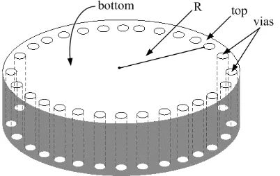
Figure 1 depicts the structure of SICC, it is constructed with top and bottom wall (conducting traces), vias array which connected the top and bottom wall. On the other hand, the operating mode of SICC should have vertical direction surface current as that ofT E101 mode in
SIW rectangular cavity for the microstrip exciting structure, soT M010
mode was selected as the working mode for its special field distribution. TheT M010 mode in SICC was characterized with revolution invariant
and z-axis irrespective if z <2.1R, it may have more flexibility than rectangular cavity in application.
It is well known that the resonant frequency (unloaded) of Circular Cavities with solid wall can be calculated by:
fmnp= c 2π√µrεr
µmn R 2 + pπ z 2
TMmnp mode
c 2π√µrεr
µmn R 2 + pπ z 2
TEmnp mode
(1)
So the corresponding resonant frequency ofT M010 is:
f010=
c 2π√µrεr ·
2.405
R =
0.383c R√µrεr
(2) whereµrandεrare relative permeability and permittivity of the filling
material used in SICC,µmn and µmn are the nth roots ofmth Bessel
function of the first kind and it’s derivative, the conductor conductivity is σ = 5.8×10⁷S/m and the loss tangent of the dielectric material is tanδ = 0.002 (30 GHz), R is the radius of the SICC with solid wall, c is the speed of light in free space.
Once the resonant frequency was given, the radius of the SICC (solid wall) can be calculated by:
R= 0.383c f010√µrεr
(3) The operating frequency was selected to be 30GHz; the permittivity of the filling material in this paper is εr = 5.7. So the corresponding
radius of the material filled SICC with solid wall can be calculated by (3), that is:
R= 0.383c
30×109√5.7 = 1.6 mm (4)
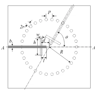
Figure 2 shows the proposed transition structure based on SICC, which consists of a SICC, a pair of identical microstrip located on top and bottom layer with an arbitrary angle ofθand two identical coupled apertures which cross at right angles with corresponding microstrip in middle layer.
Figure 2. Top view of SICC transition.
the radius of the SICC R; the length and width of aperture h, w; the radius and pitch of the via were optimized when θ = 0 with 3D Full-wave simulation tool. The initial values of above parameters were, d0 = 1 mm, l0 = 1 mm (approximately λg/4), h0 = 2 mm,
w0= 0.2 mm,R0 = 1.6 mm, the transition structure was modeled with
solid wall firstly and then the solid wall was replaced by vias-array under the guidelines of references [8–11], Some applications of SICC can be found in references [12–14], some important design guidelines can be found in [15–19]. The radius of the cavityRand the gap location d were two key parameters in designing of the transition structure; the R can be calculated with (3), and the parameterdwas approximately λg/4 ; the width of the microstrip lines were calculated to guarantee a
50 Ω impedance.
Flexibility is an important aspect should be considered in design of transition structure, the SICC based structure performed well in an arbitrary direction in different layers for the revolution-invariant field pattern distribution of the operating T M010 mode. In order
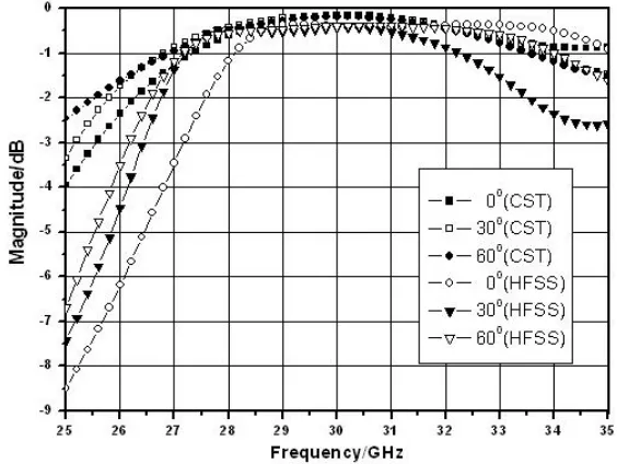
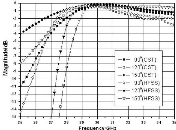
to validate the flexibility of the structure, the angle θ was set as variable parameter, simulated results aboutS11 andS21 whenθ= 30◦,
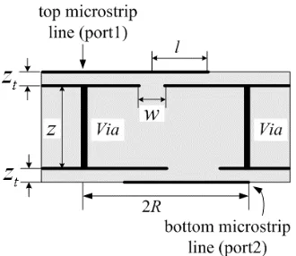
Figure 3. Lateral view of SICC transition.
Figure 4. Simulated return loss forθ <90◦.
3. SIMULATION AND RESULTS
Figure 5. Simulated return loss forθ≥90◦.
Figure 7. Simulated insertion loss for θ≥90◦.
angle of 36 degrees between two adjacent ones and the corresponding pitch is about 0.93 mm, if the radius of via was selected to be 0.2 mm. So, we have:
2r/p0.5 (5)
The condition for decreasing leakage of via walls effectively, that is
2r/p= 0.5 (6)
which mentioned in [11] can be satisfied. Return loss for different θ values of θ < 90◦ and θ ≥ 90◦ were shown in Fig. 3 and Fig. 4; the corresponding insertion loss for different θ values of θ < 90◦ and
Table 1. Dimensions of the transition structure.
d l h w R
0.6 mm 0.6 mm 2 mm 0.2 mm 1.5 mm
p r b zt z
θ≥90◦ were shown in Fig. 5 and Fig. 6. Return loss and insertion loss of the transition structure when θ= 0◦ were found to be better than −35 dB and less than 0.5 dB at the operating frequency. Return loss better than 15 dB and Insertion loss less than 0.5 dB can be observed for all the otherθvalues at the operating frequency 30 GHz. The simulated 10-dB return loss bandwidth was found to be approximately 2.5 GHz. Simulation results corresponding to two different simulation tools both show good performance between each other for the same angle ofθ in Fig. 3, Fig. 4 (return loss) and Fig. 5, Fig. 6 (insertion loss), so the predicted flexibility of the transition structure was validated.
4. CONCLUSIONS
A novel transition based on SICC (Substrate Integrated Circular Cavities) was proposed in this paper. Design method was presented for design and optimization of this transition structure. Good performance between simulated results acquire from different simulation tools was found for the proposed novel structure. Flexibility of the transition was validated by good simulation results acquired from different parameter θvalues and different simulation tools. The special transition structure was characterized with high flexibility, low insertion loss, compact structure. Some disadvantages for using of the structure, such as narrow 3-dB bandwidth and bulky dimension in a certain extent were also observed. It’s suitable for using in microwave and millimeter-wave multi-layer circuits such as LTCC module.
REFERENCES
1. Nedil, M., T. A. Denidni, and A. Djaiz, “Ultra-wideband microstrip to CB-CPW transition applied to broadband filter,” Electronics Letters, Vol. 43, No. 8, 464–466, 2007.
2. Nedil, M. and T. A. Denidni, “Ultra-wideband back-to-back CBCPW-to-CBCPW transition,” Electronics Letters, Vol. 43, No. 12, 677–678, 2007.
3. Deslandes, D. and K. Wu, “Integrated microstrip and rectangular waveguide in planar form,” IEEE Microwave and Wireless Components Letters, Vol. 11, No. 2, 68–70, 2001.
4. Deslandes, D. and K. Wu, “Analysis and design of current probe transition from grounded coplanar to substrate integrated rectangular waveguides,” IEEE Transactions on Microwave Theory and Techniques, Vol. 53, No. 8, 2487–2494, 2005.
integration of substrate integrated waveguide interconnects,” IEEE Microwave and Wireless Components Letters, Vol. 17, No. 10, 697–699, 2007.
6. Kangasvieri, T., J. Halme, J. Vahakangas, and M. Lahti, “Ultra-wideband shielded vertical via transitions from DC up to the V-band,”European Microwave Integrated Circuits Conference, 476– 479, 2006.
7. Swierczynski, T., D. A. McNamara, and M. Clenet, “Via-walled cavities as vertical transitions in multilayer millimetre-wave circuits,”Electronics Letters, Vol. 39, No. 25, 1829–1831, 2003. 8. Potelon, B., J.-C. Bohorquez, J.-F. Favennec, C. Quendo, E. Rius,
and C. Person, “Design of Ku-band filter based on substrate-integrated circular cavities (SICCs),”IEEE MTT-S International Microwave Symposium Digest, 1237–1240, 2006.
9. El-Tager, A., J. Bray, and L. Roy, “High-Q LTCC resonators for millimeter wave applications,” IEEE MTT-S International Microwave Symposium Digest, Vol. 3, 2257-2260, 2003.
10. El-Tager, A. and L. Roy, “Novel cylindrical high-Q LTCC resonators for millimeter wave applications,” IEEE MTT-S Int. Microwave Symposium Digest, Vol. 2, 637–640, 2004.
11. Cassivi, Y., et al., “Low-cost and high-Q millimeter-wave resonator using substrate integrated waveguide technique,”Proc. 32nd European Microwave Conf., Milan, Italy, September 2002. 12. Tang, H. J., W. Hong, Z. C. Hao, J. X. Chen, and K. Wu,
“Optimal design of compact millimeter-wave SIW circular cavity filter,” Electron. Lett., Vol. 41, No. 19, 1068–1069, Sept. 2005. 13. Tang, H. J., W. Hong, J. X. Chen, G. Q. Luo, and K. Wu,
“Development of millimeter-wave planar diplexers based on complementary characters of dual-mode substrate integrated waveguide filters with circular and elliptic cavities,” IEEE Transactions on Microwave Theory and Techniques, Vol. 55, No. 4, 776–782, Apr. 2007.
14. Potelon, B., J.-F. Favennec, C. Quendo, E. Rius, C. Person, and J.-C. Bohorquez, “Design of a substrate integrated waveguide (SIW) filter using a novel topology of coupling,”IEEE Microwave and Wireless Components Letters, Vol. 18, No. 9, 596–598 2008. 15. Valois, R., D. Baillargeat, et al., “High performances of shielded
LTCC vertical transitions from DC up to 50 GHz,” IEEE Transactions on Microwave Theory and Techniques, Vol. 53, No. 6, June 2005.
M. M. Tentzeris, “Low loss LTCC cavity filters using system-on-package technology at 60 GHz,”IEEE Transactions on Microwave Theory and Techniques, Vol. 53, No. 12, December 2005.
17. Eldek, A. A., “Wideband 180◦ phase shifter using microstrip-CPW-microstrip transition,” Progress In Electromagnetics Re-search B, Vol. 2, 177–187, 2008.
18. El Sabbagh, M. A., H.-T. Hsu, and K. A. Zaki, “Stripline transition to ridge waveguide bandpass filters,” Progress In Electromagnetics Research, PIER 40, 29–53, 2003.