440
Studies on Memristor Characterization based
on Non-linear Dopant Drift Model Modeled
with Window function
Prakash SavarimuthuP #
P
Department of electronics and communication Engineering, Saveetha School of Engineering, SIMATS, Thandalam, Chennai, TN – 602105, INDIA
P
#
P29TU
Abstract.
In the age of information and communication, information storage with the capability of
non-volatile low power has attracted considerable interest. Memristive devices focus on these
attributes and were achieved using nanotechnology. However, to design circuits with these
memristive devices, the characteristion needs to be described by a mathematical model. Many
models such as linear ion-drift model, non-linear ion-drift model, ThrEshold Adaptive
Memristor(TEAM) model have been proposed. These models should reasmble the physical
devices and also compute efficiently. In the present paper, the characterization of memristor
based on SPICE non-linear dopant drift model focusing on various parametric results to achieve
better i-v characteristics and power consumption compared with linear ion drift model.
INTRODUCTION
441
NON-LINEAR ION DOPANT DRIFT MODEL
The memristor representing the physical model from [2], shown in fig. 2, consists of a bilayer thin film (size D≈10nm) of TiOR2R sandwiched between platinum contacts.
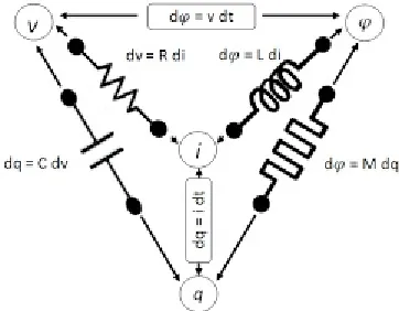
FIGURE 1. Indicates the missing gap in the passive elements now linked with the memristor.
FIGURE 2.Bilayer structure of the memristor.
Where device structure having an 'D' bilayer thickness and width of doped region of 'w'. The electric field applied to the memristor in a given direction, the boundary between the two regions is moving in the same directions. The total resistance of the memristor, RMEM, is the sum of the resistances of the doped and undoped regions,
RMEM(x)=RON x +ROFF (1-x), (1)
Where x = 𝑤
𝐷Є (0,1)
is the ratio of the width of the doped region, to the undoped region. (0 to D) represent doped area having the actual width of 'w', The relationship between the voltage and current of memristor ohm's law given by:
v(t) = RMEM(w)i(t) (2)
The rate at which the boundary movement between the doped and undoped regions depends on the resistance of doped area, on the passing current, and on other factors according to state equation[2].
𝑑𝑥
𝑑𝑡= ki(t)f(x), k =
𝜇𝑅𝑂𝑁
𝐷2 (3)
Where µ≈10P -14
P
mP 2
P
sP -1
P
VP -1
P is the so-called dopant mobility. These smaller devices at nano size can yield enormous
electric field even for small applied voltages,, which can secondarily produce significant nonlinearities in ionic transport. As a result, these can induce the rate at which the boundary between the doped to undoped regions gradually decreasing to zero. This phenomenon, called nonlinear dopant drift, can be modeled by the so-called window function f(x) given in eqn.4. This paper uses the proposed window function in the following form:
f(x) = 1- (2x-1)2p (4)
442
SPICE BASED SIMULATION RESULTS
FIGURE 3
.
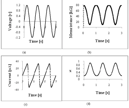
SPICE BASED MEMRISTOR CIRCUIT.Cadence-OrCAD tool used to simulate this nonlinear ion-drift model[9]. The simulated results validate memristor’s internal characteristics such as pinched hysteresis loop, φ-q characteristics. Fig. 3 shows the SPICE based Memristor circuit. The memristor was excited with sinusoidal voltage amplitude of 1.2v and frequency of 1hz. Assumed RRinitR=80kΩ, RRoffR=100kΩ, RRonR=1kΩ µ=10P
-14
P
mP 2
P
sP -1
P
VP -1
P
, p=1 and D=10nm.
FIGURE 4
.
Simulation result analyses of memristor with respect to time(a) voltage (b) memristance (c) current (d) ratio of the width of the doped region to bilayer structure.Figures 4(a-d) demonstrates the simulation result analyses of the memristor with respect to time. It can be inferred from the graphs the non-linearity of current with respect to time indicating the switching phenomenon (fig.4b). Also, the switching of memristance from high resistive state to low resistive in timefig.4c). Further, the normalized width x of the doped region is switched between the low and high levels near the limiting values of 0 and 1.
443
FIGURES 5. i-v characteristics of Memristor.
FIGURE 6. φ-q characteristics of Memristor.
RESULTS AND DISCUSSION
The effect on the frequency of the amplitude of the applied voltage, dopant mobility, applied
voltage and thickness of the thin film layer affecting the non-linear i-v curve indicates the
internal parameters of the simulated memristor which can aid in physical fabrication of
memristor and simulating memristor based circuits.
A.
Effect on the frequency of the applied voltage
FIGURE 7. i-v characteristics for different frequencies.
-40.0 -30.0 -20.0 -10.0 0.0 10.0 20.0 30.0 40.0
-1.2 -0.8 -0.4 0.0 0.4 0.8 1.2
Cu
rre
nt
[
µ
A]
Volts [V] f = 1Hz
444
In this simulation, the frequency is varied keeping the applied voltage 1.2v constant. It can be inferred from fig. 7. as frequency of the applied voltage increases the hysteresis double loop of non-linear curve diminishes and becomes a linear curve losing the memory effect.
B.
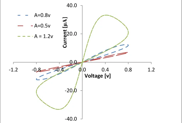
Effect of the different excitation amplitude voltage
In this simulation experiment, different amplitude excitation voltage applied by keeping the frequency 1Hz constant. As shown in fig. 8. if the amplitude of the applied voltage increases the pinched hysteresis loops also increases and vice-versa. It has been observed that increasing the amplitude voltage of 2v at f=1hz results in hard threshold switching effects[10].
FIGURE 8. i-v curve for different amplitude of the applied voltage.
C.
Effect of the thickness of the bilayer structure(D)
The simulation was carried with same amplitude voltage of 1.2v and frequency 1hz varying the bilayer thickness(D).When the thickness of the bilayer structure increased form 10nm to 100nm the non-linearity diminishes and becomes an linear curve as shown in fig. 9. The reason may be a high bias voltage is required because the distance of the doped region to cover the undoped area is larger. As a result threshold voltage of the device has not been exceeded resulting in an linear curve.
FIGURE 9. i-v curves for different thickness of bilayer structure.
-40.0 -20.0 0.0 20.0 40.0
-1.2 -0.8 -0.4 0.0 0.4 0.8 1.2
Cu
rre
nt
[
µ
A]
Voltage [v] A=0.8v
A=0.5v A = 1.2v
-40.0 -20.0 0.0 20.0 40.0
-1.2 -0.8 -0.4 0.0 0.4 0.8 1.2
Cu
rre
nt
[
µ
A]
Voltage [v] D=100N
445
D.
Effect on the mobility of ions
The experiment was repeated having the same applied voltage 1.2v and frequency of 1hz but
varying the mobility of dopant ions. Always higher the mobility of the so-called doped ions is
preferred in order for the doped region to cross the boundary as early as possible. Hence, it is
evident from the fig. 10. as the mobility of ions reduces the pinched hysteresis loop diminishes to
a linear curve. Therefore the lower the mobility of the ions decreases ionic mobility hence, as the
distance covered by the doped region is considerably less leading to an linear variation.
FIGURE 10. i-v curves for different values of mobility
E.
Power dissipation
To implement synapse (to connect between two neurons) power consumption must be low. To simulate brain requires TB of computer memory, however with memristor low power consumption is possible[11]. It can be inferred that higher the pinched hysteresis loop can be obtained with increasing voltage with increasing frequency. Therefore an optimized voltage and frequency must be chosen to retain the large sized pinched hysteresis loop. In this simulation experiment, the power dissipation for the applied voltage of 1.2v and frequency 1hz was 28.798µW indicating better power dissipation phenomenon than the linear ion-drift model[12].
FIGURE 11. Power dissipation of memristor based on non-linear dopant drift model.
-30.0 -20.0 -10.0 0.0 10.0 20.0 30.0
-1.2 -0.8 -0.4 0.0 0.4 0.8 1.2
Cu
rre
nt
[
µ
A]
Voltage [v] µ=1e-14
446
CONCLUSIONS
In this paper, characterization of memristor based on non-linear dopant drift model was simulated. This indicates simulated nonlinear ion drift model has better v-i characteristics than linear ion-drift model. Also, the effect of changing values of frequency, applied voltage, thickness and mobility are studied. Furthermore, the results indicate that the suitability of memristor in neuromorphic system which requires high computer memory density with low power dissipation can be achieved.
REFERENCES
1. Chua, L.O., Memristor-the Missing Circuit element, IEEE Transactions on circuit theory, Vol.18, No.5, 507-519, (1971).
2. S.Prakash, S.Asokan, D.B.Ghare, A guideline for designing chalcogenide materials for threshold switching”, IEEE Transactions on Electronic device letters, vol.18, no.2, 45-47, (1997).
3. S.Prakash, S.Asokan, D.B.Ghare, Easily reversible memory switching, Journal of Physics D: Applied physics, vol.29, 2004-2008, (1996).
4. Strukov, D.B, Snider, G.S, Stewart, D.R, Williams, R.S. The missing memristor found, Nature, Volume No 453, 80-83, (2008).
5. Ioannis Vourkas, and Angel Abusleme, A Digital Memristor Emulator for FPGA-Based Artificial Neural Networks, 2016 1st IEEE International Verification and Security Workshop (IVSW).
6. Pershin, Y.V., DI Ventra, M., Practical approach to programmable analog circuits with memristors, IEEE Trans. Circ.Syst.I, Volume No 57, 1857,(2010).
7. Pershin, Y.V., DI Ventra, M., Memristive circuits simulate memcapcitors and meminductors, IEEE Trans. Circ.Syst.I, Volume No 46, 517-518, (2010).
8. Manu Chilihuri, A high frequency memristor emulator circuit, M. Eng. thesis, University of Texas, Arlington, USA , Dec. 2015.
9. Biolek, Z., Biolek, D., Biolkova, V., SPICE model of memristor with nonlinear dopant drift, Radioengineering, vol.18, no.2, 210-214, (2009).
10. Pershin, Y.V., DI Ventra, M. SPICE model of memristive devices with threshold, Radioengineering, vol.18, no.2, 11-15, (2013).
11. Andy Thomas, Journal of Physics D: Appl., Phys., Vol. 46, 1-12, (2013).