Study and Defect Characterization of a Universal QCA
Gate
S.Ghosal
Department of Electronics AcharyaPrafullaChandra College, New Barrackpore,
India
D.Biswas
Department of Electrical Engineering,
Indian Institute of Technology Bombay, Powai,
Mumbai-400076, India
ABSTRACT
Quantum-dot Cellular Automata (QCA) offers a new computing paradigm in nanotechnology and is being considered as the future alternative to state-of-the art CMOS designs. The first introduced logic element, the Majority Voter (MV) led to prohibitively large and complex circuits having both uncomplemented and complemented variables. Subsequently many proposals have been made namely AOI and NNI to overcome these shortcomings. In this work we focus on a novel nanostructure (DPNNI) with double polarisation inputs which uses NAND/NOR gates as the basic building blocks, similar to conventional digital logic circuits. Simulation result shows a minimum of 43% to a maximum of 176% reduction in size of circuits with this structure in comparison to that with the AOI and NNI gates. The widespread acceptance of QCA in logic design demands investigation of defect tolerance of QCA circuit elements. Hence the defect tolerance of the proposed structure with respect to misalignment of the cells in the NAND/NOR structure have also been analyzed. Noise margin is an important figure of merit in digital circuits. The Noise Margin of this proposed structure has also been studied and it is shown to exhibit a high impedance state corresponding to a tristated structure. The fault tolerant properties of the proposed universal gate has been evaluated through simulation with QCA Designer.
General Terms
Fault Tolerance, Nand/Nor architecture, Universal Gate
Keywords
QCA, DPNNI, Noise Margin.
1.
INTRODUCTION
Over the past few decades the growth in semiconductor industry has faithfully adhered to Moore’s celebrated law whereby the component density has doubled every 18 months. However as feature size in MOS process move into DSM design various short channel effects as well as leakage current through ultrathin gate oxides seem to challenge the limits of existing CMOS technology [1]. Therefore various alternative nanostructure based designs have been proposed which seek to use the very factors limiting the growth such as the leakage tunneling current through the oxide layer. One such architecture is the quantum dot cellular automata [2], [3]. The basic logic elements of this technology are the majority voter (MV) and the inverter (INV). However, an experimental
evaluation has shown that MV is not efficiently used during technology mapping by existing logic-synthesis tools. Although it can be easily adapted to realize AND or OR, MV suffers from the disadvantage that it is not a universal gate and cannot offer the inverting function. Since at gate-level inversion is expensive in QCA (unlike conventional CMOS), built-in inversion is desirable. Moreover, it has been found that the MV is not favorable in terms of technology mapping for logic synthesis. To overcome these shortcomings various alternative structures have been proposed like AND-OR-INVERTER (AOI) and NAND-NOR-AND-OR-INVERTER (NNI) [4], [5], [6]. In this paper, the design and characterization of a novel QCA logic gate: dual polarization nand-nor-inverter (DPNNI) has been proposed. The paper presents a detailed simulation-based analysis of the DPNNI gate. The DPNNI implements a universal logic gate; and all elementary gates can be implemented using NAND/NOR building blocks as in conventional logic circuits. The AOI gate performs quite favorably, in terms of digital logic synthesis. Unlike MV, this gate is efficiently used by existing logic-synthesis tools. The experimental data on synthesis of complex designs show that using the DPNNI gate instead of AOI/NNI, results in up to 42% logic area savings. The rest of this paper is organized as follows. Section 2 is dedicated to a brief review of QCA basics and logic structure of majority voter and AOI, circuits. The Section 3 describes the proposed DPNNI gate and analyses its effectiveness on size as well as implementing standard functions. In the Section 4 QCA defect and permissible defect tolerance of the proposed AOI gate has been discussed. Section 5 gives the Results and Discussion. The simulations have been done using QCAD Designer [7].
2.
What is QCA?
Quantum-dot cellular automata (QCA) is an emerging nanotechnology that has gained significant popularity in recent years as a possible replacement for transistor circuits. University of Notre Dame researchers [Lent et al.] designed the first quantum dot cellular automata (QCA) logic gates in the early 1990’s [1]. The technology also has many powerful features, which overcome some of the most dominant problems in standard microelectronics.
2.1
Physical Structure
diagonally opposed quantum-dots. There are only two stable configurations, corresponding to the two diagonals in a square, and these two stable configurations are the two lower energy states encoding the binary values ’0’ and’1’ as shown in Fig 1. The NULL state configuration depends on the physical implementation [8][9]; for example in some cases two extra quantum-dots are placed in the center of the cell to be occupied during this state.
[image:2.595.356.496.82.321.2]
a)Logic value“0” b) Logic value “1”
Fig 1: Representation of the two logic values of a QCA cell with four quantum-dots. Black filled circles represent occupied quantum-dots while white filled circles represent
unoccupied quantum-dots.
Logic operations are performed by means of the Coulomb interactions and linear superposition of the electrical field between adjacent cells
2.2
Majority Voter
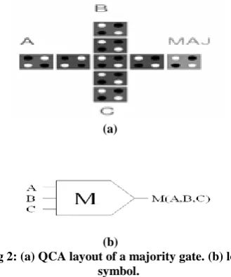
The basic logic operation is the majority voter [3] [11][12] of three inputs and the majority gate shown in Figure 2. It is described as logic function
MV (A, B, C) = AB + BC + CA
In this structure the central cell will sense the field imposed by the top, left and bottom neighboring cells by assuming a polarization equal to the polarization of the majority of these three inputs.
(a)
(b)
Fig 2: (a) QCA layout of a majority gate. (b) logic symbol.
Therefore the logic product can be performed as M(a, 0,b) and the logic sum as M(a,1, b).
2.3
AND-OR-Inverter (AOI)
This is a seven-cell gate with five input cells, one device cell, and one output cell. The gate is built from the original five
45 exhibit an inverting function.
A
B
C
D
E
F d1
d1
d2
d4
d4
d3
Fig 3(a): AOI gate layout.
A
E D
B
C
F
MV1 MV2
Fig 3(b): AOI gate Schematic
The logic function realized by the proposed AOI gate [4] is F =DE + (D + E) (A`C` +A`B +BC`)
=Maj(D,E, Maj(A`,B`C`))
where Maj() is the three-input majority function, and A` denotes the logic inversion of A. The AOI gate is logically equivalent to a concatenation of two MVs with two complemented inputs (A and C).
3.
Proposed Dual Polarization
NAND-NOR Inverter (DPNNI) Structure
A new structure to replace the majority gate as the universal building block has been proposed. It has been shown that this circuit can be used to realize NAND and NOR gate as opposed to AND/OR gate. Moreover NOT gate can also be realized. More complex functions using the above structure have also demonstrated.
The proposed structure consists of five cells (Fig 4) with a central output cell while any two of the remaining cells are used as polarizing cells and the other two as input cells. The proposed structure has a logical relationship of the form
𝐘 = 𝐋𝐓 𝐑𝐓 𝐋𝐁 + 𝐑𝐁 + 𝐋𝐁 𝐑𝐁 𝐋𝐓 + 𝐑𝐓
and 𝐘 = 𝐋𝐁𝐑𝐁 𝐑𝐓 + 𝐋𝐓 + 𝐑𝐓𝐋𝐓(𝐋𝐁 + 𝐑𝐁) Thus for RT=0; LB=0, we get 𝐘 = 𝐋𝐓 +𝐑𝐁 = 𝐋𝐓𝐑𝐁 i.e. NANDGate
[image:2.595.63.276.164.229.2] [image:2.595.82.247.452.650.2]Fig 4: The DPNNI structure
FOR LT=1; RB=0; RT=0 and LB as the input cell we get the NOT GATE. Moreover for certain input combinations the high impedance tristated state Z can be expressed as
which is manifested as neither HIGH, nor LOW polarization on simulation. The high impedance state is essential for realization of tristated logic which allows several devices to timeshare a common wire called a bus.
3.1
Characteristics of the Proposed
NAND/NOR Structure
The MV can be easily adapted for the realization of AND, OR gates but it lacks from the requisites to be treated as a universal gate.
3.1.1 Realization of NAND/NOR
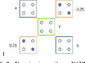
The layout and the schematic of the proposed structure to realize a NAND and NOR gate has been shown in Fig 5a and Fig 6a respectively. The structure consists of five cells consisting of two input cells, one processing/output cell and two polarizing cells. All the cells are placed at an angle of 450 with respect to the processing cell y. The polarization value may be considered to be ± 0.75 as opposed to ± 1 as in MV and AOI which represents partial confinement of the electrons. For the NAND gate the left top (LT) and right bottom (RB) cells are taken as the input cells while the other two as polarizing cells. For the NOR gate left top (LT) and left bottom (LB) cells are taken as the input cells
[image:3.595.53.172.86.188.2]I
Fig 5a: New structure acting as NAND gate
In a similar manner the INVERTER can be realized using LT=1; RB=0; RT=0 and LB as the input cell. The realization of other standard functions using this structure can be done as tabulated below in table 1.
Fig 5b: Simulation output of the proposed NAND gate
[image:3.595.366.491.321.423.2]
Fig 6a: New structure acting as NOR gate
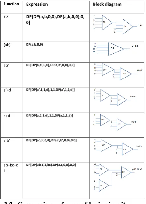
[image:3.595.313.533.488.671.2] [image:3.595.88.228.521.625.2]Table 1 Logic synthesis of some standard functions
Function Expression Block diagram
ab DP[DP(a,b,0,0),DP(a,b,0,0),0, 0]
(ab)’ DP(a,b,0,0)
ab’ DP*DP(a,b’,0,0),DP(a,b’,0,0),0,0+
a’+d DP*DP(a’,1,1,d),1,1,DP(a’,1,1,d)+
a+d DP[DP(a,1,1,d),1,1,DP(a,1,1,d)]
a’b’ DP*DP(a’,b’,0,0),DP(a’,b’,0,0),0,0+
ab+bc+c a
DP[DP(ab,1,1,bc),DP(a,c,0,0),0,0]
3.2
Comparison of area of logic circuits
designed using MV, AOI and NAND/NOR
structure
In this work the next focus is to describe the effective size of the gate shown in Fig. 4. The effective area is calculated with sum of all cell size with permissible distance. The total area of the proposed structure as shown in Fig 4, considering the cell size to be (20nmX20nm) and spacing between each cells as 2nm is (68nmX68nm=4624nm2). All the cells are placed at an angle of 450 with respect to the processing cell y. Using cells of similar size as used here and a similar inter-cell spacing the AOI has an effective area of 13750 nm2 [4]. A modified AOI [6] later proposed has an effective area (110nm X 68nm) of 7480nm2 which basically reduce the size of AOI gate by 54% of previous proposal. It was reported that the Effective area of MV is 8100nm2. The Table 2 shows the evaluation of the effectiveness of our proposal by means of logic synthesis using the DPNNI. Our proposal provides a robust and more compact alternate option to design versatile logic function. Assuming that the effective area of MV is Ea (in nm
2
) then the effective area of modified AOI is 0.92Ea. As the area of the
proposed structure is much lesser compared to the majority voter and the AOI we tried to find out the same comparison among some benchmark circuits designed using the 3 different structures. The Table 2 shows the comparison. From the above table it is noted that there is a reduction of area by atleast 43% using the new structure compared to that designed using MV and the modified AOI. The effect of
Table 2 Comparison of effective area of MV, AOI and DPNNI for some standard functions
Design using MV Design using AOI Design using DPNNI
N I n v
Ea N I
n v
Ea Impr N I
n v
Ea Impr
1 0
1 1 0 0.92 8% 1 1 1.31 -31%
1 1
1.57 1 1 1.31 26% 1 0 .57 100%
1 1
1.57 1 1 1.49 8% 1 1 1.14 43%
1 1
1.57 1 1 1.49 8% 1 1 1.14 43%
a+b 1 0
1 1 0 .92 8% 1 0 .57 43% 1 2
2.33 1 2 2.07 26% 1 0 .57 176%
4 0
4.88 4 0 5.55 -13.7 %
4 0 4.39 49%
4.
Faults in QCA Circuits
The small size of QCA based systems combined with their manufacturing methods (such as self assembly) are substantially different from CMOS and make them more susceptible to defects [13]14] and faults.In the present stage of QCA manufacturing, defects are possible in both synthesis phase and deposition phase. Manufacturing defects during synthesis may cause a cell to have missing or extra dots or/and electrons. However defects are much more likely to occur in the deposition part than in the synthesis part which will result in cell misplacement.In addition defects in QCA manufacturing may well manifest themselves differently at logic level than CMOS. Defect characterization [15] [16] is therefore vital to design and test of QCA systems.
4.1
Defect Characterization
Defect characterization in QCA circuits[19] may be classified in the following manner.
[image:4.595.314.543.605.702.2]4.2
Noise Margin
The noise in the context of digital circuits means unwanted variations of voltages and currents at the logic nodes. The electrical function of a gate is best expressed by its VTC which plots the output voltage as a function of the input voltage. These deviations can be caused by noise or by the loading on the output of the gate. The regions of acceptable high and low voltages are delimited by the VIH and VIL
voltage levels respectively. The region between VIH and VIL is
called the undefined region (transition width). The two other points VOL and VOH determine the noise margins of the
inverter. These are the maximum permitted logic-0 or “low” level at the input, VIL, and the maximum permitted logic-1 or
“high” level at the input, VIH .
For a gate to be robust and insensitive to noise disturbances, it is essential that the “0” and “1” intervals be as large as possible. A measure of the sensitivity of a gate to noise is given by the noise margins NML (noise margin low) and NMH
(noise margin high), which quantize the size of the legal”0” and “1”, respectively, and set a fixed maximum threshold on the noise value: NML=VIL-VOL and NMH=VOH-VIH
where-NML= Noise margin for low input; NMH=Noise
margin for high input. Here the strength of the polarizing cell has been continuously varied to find a threshold value beyond which the circuit ceases to give a well defined output even for the same strength of inputs.
5. Result and Discussion
As the NAND/NOR, structure can be considered as the universal logic block in the design of QCA circuits, the assessment of defect tolerance of such devices is most desirable. We analyze the defective behavior of the proposed structure as well as their sensitivity to the polarizing levels x-axis: displacement in nm
[image:5.595.329.527.71.189.2]y-axis: output voltage in volt
Fig 7a:Displacement sensitivity of A cell in NOR gate
[image:5.595.329.526.212.337.2]Fig 7b:Displacement sensitivity of B cell in NOR gate
[image:5.595.322.533.372.646.2]Fig 7c:Displacement sensitivity of top polarisation cell in NOR gate
Fig 7d:Displacement sensitivity of bottom polarisation cell in NOR gate
[image:5.595.53.250.481.598.2]Fig 8a:Displacement sensitivity of A cell in NAND gate
[image:6.595.60.275.68.595.2]Fig 8b:Displacement sensitivity of B cell in NAND gate
[image:6.595.328.528.70.199.2]Fig 8c:Displacement sensitivity of top polarising cell in NAND gate
[image:6.595.311.546.238.325.2]Fig 8d:Dispalcement sensitivity of bottom polarisation cell in NAND gate
Fig 8e:Polarisation sensitivity(Noise Margin) of NAND gate
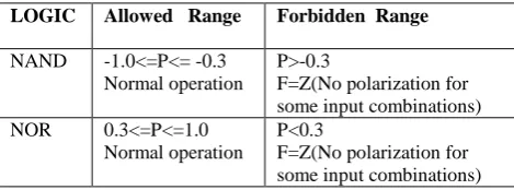
Table 3: Polarization sensitivity (NOISE MARGIN)
LOGIC Allowed Range Forbidden Range
NAND -1.0<=P<= -0.3 Normal operation
P>-0.3
F=Z(No polarization for some input combinations) NOR 0.3<=P<=1.0
Normal operation
P<0.3
F=Z(No polarization for some input combinations)
A comparative study of the structures [4][10][12] reveals the following facts. While the majority voter suffers from the drawback of having no provision for an inverter and has to rely on displaced wire chain for inversion. As a result for circuits involving complemented variables the effective circuit area becomes larger. The AOI [4] while having the inherent provision for inversion suffers from the problem of unequal spacing of input and output binary wires- that is, in fixing the distances d1, d2 and d3 of Fig. 3(a).This would pose problem in large scale implementation of such an asymmetrical structure Moreover And-Or-Inverter is not a universal gate. All Boolean functions cannot be designed using only A-O-I gate. Another drawback of A-O-I gate is that it requires more space and the A-O-I gates and circuits using AOI are more complex nature compared to that of MV or NOT gates. The tile based structures while being robust take considerably more space. Besides all these drawbacks of AOI, an important advantage of using a NAND based circuit is that the existing logic minimization rules are NAND /NOR based hence the DPNNI offers an inherent advantage as its basic building block is a NAND gate. Moreover a NAND [18] actually propagates an improved error probability due to its logic properties through its natural computation.
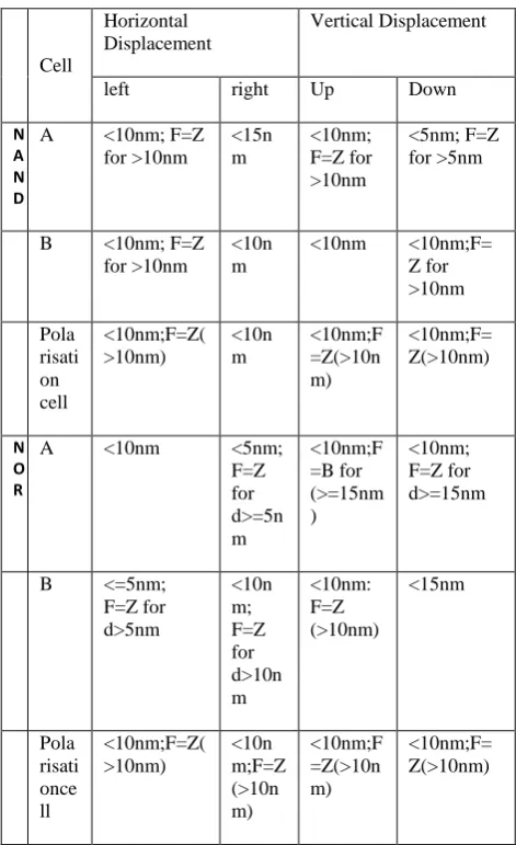
Table 4: Displacement sensitivity of cells on DPNNI structure
8.
REFERENCES
[1] International technology roadmap for semiconductors: 2001, Semiconductor Industries Association, San Jose, CA,
[2] C. S. Lent, P. D. Taugaw, W. Porod, and G. H. Bernstein,” Quantum cellular automata,” Nanotechnology, Vol.4, pp.49-57, 1993.
[3] C. S. Lent and P. D. Tougaw, 1997 “A device architecture for computing with quantum dots,” Proc. IEEE, vol. 85, no. 4, pp. 541–557.
[4] Momenzadeh,M; Jing Huang Tahoori; M.B.Lombardi, “Characterization,test and logic synthesis of and-or-inverter(AOI) gate design for QCA implementation,” IEEE Trans. Computer-Aided Design of integrated Circuits and Systems,vol.24,pp1881-1893,12,Dec.2005
[5] B.Sen and B.K.Sikdar,”Characterisation of universal Nand-Nor-Inverter QCA gate”11th IEEE VLSI Design and Test Symposium,Kolkata,August 8-11,2007
[6] Kunal Das and Debashis De “A Novel Approach for AOI gate design for QCA”,International conference on Computers and Devices for Communication ,2009 [7] K. Walus. (2002) ATIPS Laboratory QCADesigner
Homepage. ATIPS Laboratory, Univ. Calgary, Calgary,
Canada. [Online].
Available:http://www.atips.ca/projects/qcadesigner [8] I. Amlani et al.,2000 “Experimental demonstration of a
leadless quantum-dot cellular automata cell,” Appl. Phys. Lett., vol. 77, no. 5, pp. 738–740.
[9] A. Orlov et al.,2000 “Experimental demonstration of clocked single-electron switching in quantum-dot cellular automata,” Appl. Phys. Lett., vol. 77, no. 2,pp. 295–297.
[10] K.Walus, Schulaf and Julliaen et al, 2004 “Circuit design based on majority gates for application with Quantum dot cellular automata” in Proc IEEE Nanotechnology conf, vol 4, page 1350- 135.
[11] I. Amlani, A. O. Orlov, G. Toth, C. S. Lent, G. H. Bernstein and G.L. Snider, “Digital logic gate using quantum-dot cellularautomata,” Applied Physics Letters, pol. 74, pp. 2875, 1999
[12] Tougaw, P. Douglas, Lent, Craig S,” Logical devices implemented using quantum cellular automata”, Journal of Applied Physics75(3): Feb 1, 1994, pp1818-1825.M. Momenzadeh, M. Ottavi, F. Lombardi, “Modeling QCA defectst molecular level in combinational circuits,” in Proc. DFT in VLSISystems, Monterey, CA, USA, Oct. 2005, pp. 208–216.
[13] M.B Thoori, J.Huang, M.Momenzadeh, and .Lombardi, ”Testing of quantum Cell automata” IEEE Trans. Nanotechnol.,vol.3, no4. pp432-442,Dec.2004
[14] M. B. Tahoori, M. Momenzadeh, J. Huang, and F. Lombardi, “Def ects and faults in quantum cellular automata at nano scale,” in Proc. VLSI Test Symp., Napa Valley, CA, 2004, pp. 291–296.
[15] A.Fijany and B.N.Toomarian, “New design for quantumdot cellular automata to obtain fault tolerant logic gates”Journal of Nanoparticle Res.,vol.3 ,pp 27-37,2001
[16] Bo Mar, Jason George, Paul Hassler “Error immune logic for low power probabilistic computing”VLSI Design 2010 Article ID 460312
[17] S.Karthigai Lakshmi and G.Athistha”Efficient Design of Logical Structures and Functions using nanotechnology based Quantum dot cellular automata design”,Int.Journ of Comp.Appl. vol3,No.5,2010
[18] Edts:F.Lombardi,J.Huang Artech House “Design and Test of Digital circuits by Quantum dot Cellular automata”
Cell
Horizontal Displacement
Vertical Displacement
left right Up Down
N A N D
A <10nm; F=Z for >10nm <15n m <10nm; F=Z for >10nm <5nm; F=Z for >5nm
B <10nm; F=Z for >10nm
<10n m
<10nm <10nm;F= Z for >10nm Pola risati on cell <10nm;F=Z( >10nm) <10n m <10nm;F =Z(>10n m) <10nm;F= Z(>10nm) N O R
A <10nm <5nm; F=Z for d>=5n m <10nm;F =B for (>=15nm ) <10nm; F=Z for d>=15nm
[image:7.595.48.284.116.502.2]