Design and Simulation of Decoder Unit of 32-Bit
RISC Processor
Mrudul S. Ghaturle1, Prof. R. D. Kadam2
1
M-Tech (Student) ,E&T Department, BDCOE, Sevagram
2
Assistant Professor, E&T Department, BDCOE, Sevagram
Abstract: The paper proposes 32-bit RISC processor with floating point arithmetic for high speed and low power consumption .It is having five stage pipelining which is designed using VHDL. Number of instruction are designed for this processors. We use 5-stage pipelining which involves instruction fetch module, instruction decode, module, execution module, memory i/o and write block. This paper focuses on the decoder unit which is having different instruction formats for different type of instructions. Keywords: RISC processor, floating point arithmetic, VHDL.
I. INTRODUCTION
The processor in a personal computeror embedded in small devices is often called a microprocessor. Types of processors according to the Instruction
set:-A. CISC (Complex Instruction Set Computing)
RISC (Reduced instruction set computing) The RISC Processor have reduced number of Instructions, fixed instruction length, more general purpose registers, load-store architecture and simplified addressing modes which makes individual instructions execute faster, achieve a net gain in performance and an overall simpler design with less silicon consumption as compared to CISC.RISC design ideally suited to participate in a powerful trend in the embedded Processor market - the "system-on-a-chip". The most common RISC microprocessors are ARM, SP ARC, MIPS and IBM's PowerPC. Some CPUs have been specifically designed to have a very small set of instructions – but these designs are very different from classic RISC designs, so they have been given other names such as minimal instruction set computer (MISC), or transport triggered architecture (TTA), etc. Despite many successes,
RISC has made few inroads into the desktop PC and commodity server markets, where Intel's x86platform remains the dominant
processor architecture .Outside of the desktop arena, however, the ARM architecture (RISC) is in widespread use in smartphone, tablets and many forms of embedded device. It is also the case that since the Pentium Pro (P6) Intel has been using an internal RISC processor core for its processors. While early RISC designs differed significantly from contemporary CISC designs, by 2000 the highest performing CPUs in the RISC line were almost indistinguishable from the highest performing CPUs in the CISC line[9].
II. DECODER
The first stage of a pipelining is instruction fetch (IF) stage. The operation of the IF stage starts when the ROM (Read Only Memory) fetch the instruction from text files. When the instruction is fetched from the IF stage, the opcode is sent to the decoder unit. ID stage sends control command to other units of processor based on opcode of the instruction. Branch unit is also included in ID stage. Input of ID stage is from IF stage.ID stage includes four instruction formats
A. R-Type (Register type)
B. I-Type (Immediate type )
C. J-Type (Jump type)
D. I/O-Type (Input-Output type)
III. MIPS INSTRUCTION SET
MIPS design consist four types of instruction set. Register type, immediate type and Jump type and Input-output. The instruction format is shown in the below figure, respectively
Volume 5 Issue VII, July 2017- Available at www.ijraset.com
©IJRASET (UGC Approved Journal): All Rights are Reserved
931
[image:3.612.203.411.245.331.2]Figure 1. R-Type Instructions Format
Figure 1 shows R-Type instruction format. Here last 6 bits represents the opcode. Next 15 bits represents 3 registers Rs, Rt and Rd respectively, on which operations are performed. Rs, Rt are source registers and Rd is the destination registers respectively. Next 5 bits is shift amount which is point to the number of bits to be shifted. Last 6 bits is function field points to the function that needs to be perfomed on the registers.The data path for R-Type instruction can be depicted as follows in figure 2. It is used mainly for ADD, SUB and OR operation. E.g. add Rd, Rs, Rt. Here signed addition contents of (Rs) + (Rt) is saved into Rd.
Figure 2. Datapath for R-Type Instructions Format
B. Immediate Type(I-Type)
Figure 3. I-Type Instructions Format
Figure 3 shows I-Type instruction format. Similar to Rtype, first 6 bits represents the opcode and next 10 bits represents Rs, Rt respectively. Here Rs is source register and
also note that Rt is source register for store and destination register for load operation. Last 16 bits represents immediate value which is a part of instruction but not part of memory.
Figure 4. Datapath for I-Type Instructions Format
The data path for I-Type instruction can be depicted as follows in figure 4. It shows that Rt register can be used both as source and destination accordingly and lastl6 bits is the
immediate value sent to sign extend and then to ALU, for performing the required operation. It is used for ADD!, AND!, and ORI operation. E.g. addi Rt, Rs,Here (Rs) + 5 is stored in the destination register Rt. 5 is
[image:3.612.198.414.510.619.2]C. Jump Instruction(J-Type)
Figure 5. J-Type Instructions Format
Figure 5 shows J-Type instruction format. First 5 bits of this instruction format represent the type of branch operation to be performed. The remaining 26 bits represents the branch offset in 2's complement format. This number is added to the value of the PC to obtain the branch target address .In figure 6 shows functionality of J -type instruction. It shows that the last four bits of PC+4 are appended to the shift left by 2 value of the 26-bit instruction, taken from Instruction Memory, to get the 32-bit jump address. E.g. j trgt. Here, j is jump instruction word and trgt is target. It skips the other instructions and jumps to the target.
Figure 6. Datapath for J-Type Instructions Format
[image:4.612.202.407.247.327.2]D. Input-output Type(I/O-Type)
[image:4.612.206.408.384.431.2]Figure 7. I/o-Type Instructions Format
Figure shows Input-output Instruction format for giving the input and obtaining the output.
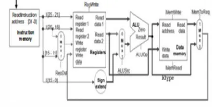
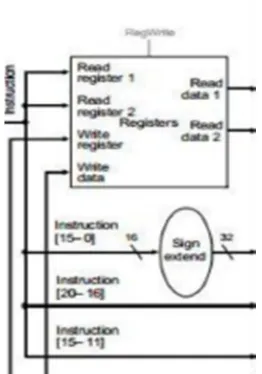
E. Block Diagram
[image:4.612.241.372.511.698.2]Volume 5 Issue VII, July 2017- Available at www.ijraset.com
©IJRASET (UGC Approved Journal): All Rights are Reserved
933
F. RTL View 1) Decoder:
G. Simulation 1) Decoder:
IV. CONCLUSION
In decoder module by the use of instruction formats (R-type, I-type, J- type, I/o-type) and datapths ,the execution of any instruction becomes faster and errorless. It is easy to edit &debug.
REFERENCES
[1] Sarika U. Kadam, S. D. Mali, “Design of Risc Processor using VHDL”, 2016International Journal of Research Granthaalaya, Vol.4 (Iss.6): June, 2016, DOI:10.5281/zenodo.56647.
[2] Swati Joshi ,Sandhya Shinde,Amruta Nikam, “32-bit pipeline Risc Processor in VHDL using Booth Algorithm ,”International Research Journal of Engineering and Technology(IRJET),e-ISSN: 2395 -0056, Volume: 03 Issue: 04 | April-2016 ,pp.2484-2487
[3] Vishwas V.Balpande ,Vijendra P.Meshram,Ishan A. Patilm,Sukeshini N.Tamgadem,Prashant Wanjari, “Design and Implementation of RISC processor on FPGA,”Indian Journal of Advanced Research in computer science and software Engineering, ISSN:2277 128xVol 9(8),Volume 5,Issue 3,March 2015,pp.1161-1165
[4] Soumya Murthy, Usha Verma, “FPGA based Implementation of Power Optimization of 32 Bit RISC Core using DLX Architecture,” 2015 International Conference on Computing Communication Control and Automation, DOI 10.1109/ICCUBEA.2015.19
[5] Mohit N. Topiwala, N. Saraswathi , “Implementation of a 32-bit MIPS Based RISC Processor using Cadence,” 2014 IEEE International Conference on Advanced Communication Control and Computing Technologies (ICACCCT), ISBN No. 978-1-4799-3914-5/14/©2014 1EEE.
[6] Mrs. Rupali S. Balpande,Mrs. Rashmi S. Keote, “Design of FPGA based instruction Fetch and Decode Module of 32-bit (MIPS) processor,” International Conference on communication Systems and Network Technologies,DOI:10.1109/CSNT.2011.91,2011
[8] Sharda P. Katke, G.P. Jain,"Design and Implementation of 5 Stages Pipelined Architecture in 32 Bit RISC Processor", IJETAE, Volume 2. Issue 4 April 2012, pp. 340-346
[9] RISC, CISC and Floating point Wikipedia
[10] Kui YI, Yue-Hua DING, “32-bit RISC CPU Based on MIPS Instruction Fetch Module Design”, 2009 International Joint Conference on Artificial Intelligence, 978-0-7695-3615-6/09, 2009 IEEE
[11] Gautham P, Parthasarathy R. Karthi, Balasubramanian. "Low Power Pipelined MIPS Processor Design," in the proceedings of the 2009, l2th international symposium,2009 pp. 462-465
[12] Neenu Joseph. Sabarinath. S. "FPGA based Implementation of High Performance Architectural level Low Power 32-bit RISC Core", 2009 IEEE [13] Harpreet Kaur, Nitika Gulati, "Pipelined MIPS With Improved Datapath", IJERA, Vol. 3, Issue 1, January -February 2013, pp.762-765
[14] Pejman Lotfi-Kamran. Ali-Asghar Salehpour. Amir-Mohammad Rahmani. Ali Afzali-Kusha, and Zainalabedin Navabi. "Dynamic Power Reduction of Stalls in Pipelined Architecture Processors", International Journal Of Design, Analysis And Tools For Circuits And Systems. Vol. I, No. I, June 2011.