N A N O E X P R E S S
Open Access
Effect of etching time on morphological, optical,
and electronic properties of silicon nanowires
Nesma Nafie, Manel Abouda Lachiheb and Mongi Bouaicha
*Abstract
Owing to their interesting electronic, mechanical, optical, and transport properties, silicon nanowires (SiNWs) have attracted much attention, giving opportunities to several potential applications in nanoscale electronic,
optoelectronic devices, and silicon solar cells. For photovoltaic application, a superficial film of SiNWs could be used as an efficient antireflection coating. In this work we investigate the morphological, optical, and electronic
properties of SiNWs fabricated at different etching times. Characterizations of the formed SiNWs films were performed using a scanning electron microscope, ultraviolet–visible-near-infrared spectroscopy, and light-beam-induced-current technique. The latter technique was used to determine the effective diffusion length in SiNWs films. From these investigations, we deduce that the homogeneity of the SiNWs film plays a key role on the electronic properties.
Keywords:Silicon nanowires, Reflectivity, Light-beam-induced-current, Diffusion length
Background
Silicon nanowires (SiNWs) have attracted much atten-tion in the recent years due to their importance in the field of electronic devices and photovoltaic [1-4]. Hence, SiNWs could be used as an antireflection coating due to the reduction of optical loss which is an important factor to obtain efficient Si solar cells. However, when SiNWs are used as an antireflection coating, a great care should be taken to avoid degradation of the elec-tronic properties, which in turn can increase the serial resistance of the solar cell. Different methods have been employed to fabricate SiNWs, such as chemical physical deposition [5], laser ablation [6,7], thermal evaporation [8,9], and etching. In this paper, we used the silver-assisted chemical etching technique [10-15]. We fabri-cate SiNWs at different durations, ranging from 10 to 90 min.
Methods
Substrates used in this study are P+ silicon wafers, boron-doped and (100) oriented, with thickness of 500 μm and resistivity of 0.01 to 0.02 Ωcm. After
cleaning, silicon samples were immersed into the etching solution containing 0.05 M AgNO3, 40% HF, and H2O2 at room temperature for different etching times; 10, 20, 30, 40, 50, 60, 70, 80, and 90 min. After etching, samples were rinsed with deionized water to remove residual HF and immersed in a H2O-HNO3 (2 and 1 V) solution during several seconds to remove the silver film.
The morphology of samples was analyzed using a scanning electron microscope (SEM). We performed top and cross-section SEM images of the samples. The cross-section SEM images were used to evaluate the length of SiNWs. We measured the surface reflectivity in the 250 to 1,250 nm spectral range by a UV–vis-NIR spectrophotometer. To study the electronic properties of the formed films, we evaluate the effective diffusion lengths (L) of minority carriers in the SiNWs films. Values of L were carried out from the light-beam-induced-current (LBIC) profiles measured on metal/ SiO2/SiNWs/c-Si/metal diode.
Results and discussion
In Figure 1 we give the top SEM views of one sample, before (Figure 1a) and after (Figure 1b) removing the sil-ver film. One can see in Figure 1a, the silsil-ver dendrites formed during the etching process. In Figure 1b, we give a tilted SEM view of the SiNWs after removing the Ag * Correspondence:[email protected]
Laboratoire de Photovoltaique, Centre de Recherches et des Technologies de l’Energie, Technopole de Borj-Cedria, BP 95, Hammam-Lif, Tunis 2050, Tunisia
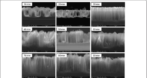
film. In Figure 2, we give cross-sectional SEM images of SiNWs films prepared at 10, 20, 30, 40, 50, 60, 70, 80, and 90 min etching times. As reported in Figure 3, the mean length of the film varies from 21 to 38 μm. From Figure 3, we notice that the etching velocity is similar for 10, 20, and 30 min. However, it is more important for 40 and 50 min, where the maximum length is reached. When the sample is etched at greater durations, the length decreases by 10μm from its maximum value and seems to be stabilized at values around 28μm. This was attributed to the fact that when the etching process started, the HF solution etches the silicon substrate lead-ing to an increase of the SiNWs’ length. After reaching the maximum length at 50 min, SiNWs themselves are
etching by the HF solution as observed in the SEM image corresponding to 60 min.
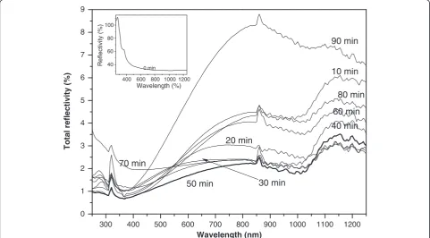
The total reflectivity in the 250 to 1,250 nm spectral range of formed films has very low values, less than 1% in the UV domain and a maximum of 8% in the visible and near-infrared regions (Figure 4). Generally, radiations with small wavelengths (UV domain) are absorbed at small depth and this absorption depends on the surface morphology. In the case of the non-treated sample, the reflectivity in the UV region is greater than 50% as shown in the inset of Figure 4. However, values of the reflectivity of SiNWs films in the UV domain are in the 0.5% to 1.5% range, which is unusual in silicon, even with texturized morphology
[image:2.595.63.539.89.238.2](a) (b)
[image:2.595.56.540.456.714.2]Figure 1Top SEM views of one sample.(a) Before, and (b) after removing the silver film.
and/or porous silicon. This was attributed to the im-portant internal surface area of SiNWs. From curves in Figure 4, we remark that in the fully used spectral range, the SiNWs film elaborated at 50 min has the minimum value of the total reflectivity. The small values of reflectivity are attributed to the multiple reflections of incident photons which are important when the length of SiNWs film is important (38 μm during 50 min).
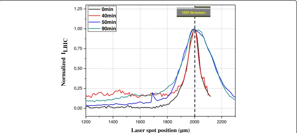
For the electronic characterization, we use the LBIC technique at the He-Ne wavelength. A schematic illus-tration of the LBIC technique is given in Figure 5. LBIC measurements were performed on metal-insulator-semiconductor structures formed on SiNWs films. Typ-ical LBIC profiles are given in Figure 6. We notice that we obtained the same shape of LBIC profiles for samples etched during 30, 50, 60, 70, 80, and 90 min. However, for samples etched during 10, 20, and 40 min, the LBIC profiles have approximately the same shape of that one performed on the MIS diode without SiNWs (0 min). Using the LBIC measurements (ILBIC), we determine the effective values of L. To carry out L values, we fit the LBIC theoretical expression given in Equation 1 [16] to the measured LBIC profiles.
ILBIC /expð x LÞ
x3
2 ð
1Þ
Obtained values of the effective diffusion length are plot in Figure 7. We remark that the obtained Lvalues can be divided into two domains: red and green regions in Figure 7. The red region corresponds to theLvalues obtained for samples prepared during 0, 10, 20, and 40 min. The green region corresponds to samples pre-pared at 30, 50, 60, 70, 80, and 90 min.
To understand whyLvalues change from a sample to another, we use the cross-section SEM images of Figure 2
300 400 500 600 700 800 900 1000 1100 1200 0 1 2 3 4 5 6 7 8 9
400 600 800 1000 1200 40 60 80 100 Reflectivity (%) Wavelength (%) 0 min
Total reflectivity (%)
[image:3.595.56.290.88.265.2]Wavelength (nm) 90 min 10 min 80 min 60 min 40 min 50 min 70 min 30 min 20 min
Figure 4Total reflectivity spectra of all SiNWs films in the 250 to 1,250 nm wavelength range.The inset is the total reflectivity of untreated silicon surface.
0 10 20 30 40 50 60 70 80 90 100 20 22 24 26 28 30 32 34 36 38 40
Length of SiNWs (µm)
[image:3.595.57.539.437.703.2]Etching time (min)
and the total reflectivity of films given in Figure 4. In Figure 2, we remark that durations 10, 20, and 40 min lead to inhomogeneous SiNWs films. However, the cross-section SEM images of samples prepared during 30, 50, 60, 70, 80, and 90 min show homogeneous films. In addition, taken into account that at the used wave-length in the LBIC investigations (He-Ne: 633 nm), the corresponding values of the total reflectivity (Figure 4) cannot explain, for example, why theLvalue of the sam-ple prepared at 90 min is greater than that one prepared at 30 min. Consequently, we attribute these variations not to the total reflectivity, but to the carriers’trapping at surface defects. For this purpose, we consider the schemes given in Figure 8. Thus, when the MIS diode
contains homogeneous SiNWs, a great amount of photo-generated electrons by the laser beam can reach the top metal contact. However, when SiNWs are not homogeneous, surface recombination at small wires reduces the LBIC current value, leading to a decrease in the effective diffusion length.
Conclusions
In this study, we present a morphological, optical, and electronic study of SiNWs films elaborated at different durations; 10, 20, 30, 40, 50, 60, 70, 80, and 90 min. At some etching durations, a regular structure of formed SiNWs was observed. The SiNWs lengths vary from 21 to 38μm. We notice a spectacular very low value of the Si
SiNWs
Generation volume Laser
beam
Ag/Al contact
Ag/Al contact
[image:4.595.59.539.89.268.2]ILBIC
Figure 5Schematic illustration of the LBIC technique.
1200 1400 1600 1800 2000 2200
0,00 0,25 0,50 0,75 1,00 1,25
Normalized I
LBIC
Laser spot position (µm) 0min
40min 50min 90min
[image:4.595.58.539.499.714.2]MIS Structure
total reflectivity reaching a minimum less than 1% in the 250 to 400 nm and a minimum of 1.5% in the visi-ble domain. From LBIC investigations, we deduce that the homogeneity of the SiNWs film plays a key role on the electronic properties. Hence, we carried out that when the SiNWs film is inhomogeneous, surface re-combination of photo-generated carriers can decrease the effective diffusion length.
Competing interests
The authors declare that they have no competing interests.
Authors’contributions
NN prepared samples, MIS diodes, and performed SEM images. She also achieved the reflectivity and LBIC measurements. MAL helped on the preparation of samples, SEM investigations, carrying out the length of SiNWs, and the interpretation of LBIC profiles. Finally, MB supervised the work, did the interpretations, and wrote the text with NN and MAL. All authors read and approved the final manuscript.
Received: 27 April 2012 Accepted: 8 June 2012 Published: 16 July 2012
References
1. Zhao XY, Wei CM, Yang L, Chou MY:Quantum confinement and electronic properties of SiNWs.Phys Rev Lett2004,92:236805.
2. Ma DDD, Lee CS, Au FCK, Tong SY, Lee ST:Small diameter SiNWs.Science 1874,2003:299.
3. Li DY, Wu YY, Kim P, Shi L, Yang PD:Thermal conductivity of individual SiNWs.Appl Phys Lett2003,83:2934.
4. Cui Y, Lieber CM:Functional nanoscale electronic devices assembled using SiNWs building blocks.Science2001,291:851.
5. Westwater J, Gosain DP, Tomiya S, Usui S, Ruda H:Growth of silicon nanowires via gold/silane vapor–liquid–solid reaction.J Vac Sci Technol B 1997,15:554.
6. Morales AM, Lieber CM:A laser ablation method for the synthesis of crystalline semiconductor nanowires.Science1998,279:208.
7. Wang N, Zhang YF, Tang YH, Lee CS, Lee ST:SiO2-enhanced synthesis of Si nanowires by laser ablation.Appl Phys Lett1998,73:3902.
8. Yu DP, Bai ZG, Ding Y, Hang QL, Zhang HZ, Wang JJ, Zou YH, Qian W, Xiong GC, Zhou HT, Feng SQ:Nanoscale silicon wires synthesized using simple physical evaporation.Appl Phys Lett1998,72:3458.
9. Zhang YF, Tang YH, Lam C, Wang N, Lee CS, Bello I, Lee ST:Bulk quantity Si nanowires synthesized by SiO sublimation.J Cryst Growth2000,212:115. 10. Peng KQ, Yang YJ, Gao SP, Zhu J:Synthesis of large-area silicon nanowires
arrays via self-assembling nanoelectrochemistry.Adv Mater2002,14:1164. 11. Peng K, Yung Y, Gao S, Zhu J:Dendrites-assisted growth of silicon
nanowires in electroless metal deposition.Adv Funct Mater2002,13:127. 12. Peng K, Fung H, Hu J, Wu Y, Zhu J, Yun Y, Lee ST:Metal-particle-induced,
highly localized site-specific etching of Si and formation of single-crystalline Si nanowires in aqueous fluoride solution.Chem Eur2006, 12:7942.
13. Srivastava SK, Kumar D, Singh PK, Kar M, Kumar V, Husain M:Excellent antireflection properties of vertical silicon nanowire arrays.Sol Energ Mater Sol Cells2010,94:1506.
0 10 20 30 40 50 60 70 80 90 100
70 75 80 85 90 95 100 105 110 115 120 125 130 135 140
L (
µ
m
)
Etching time (min)
Values of L for homogeneous
SiNWs film
[image:5.595.56.545.92.395.2]Values of L for inhomogeneous SiNWs film
Figure 7Obtained values of the diffusion length vs. etching time.
MIS diode with homogeneous SiNWs
MIS diode with inhomogeneous SiNWs
[image:5.595.305.540.471.740.2]14. Peng KQ, Xu Y, Wu Y, Yan Y, Lee ST, Zhu J:Aligned single-crystalline Si nanowires arrays for photovoltaic applications.Small2005,11:1062. 15. Peng KQ, Wu Y, Fang H, Zhong XY, Xu Y, Zhu J:Uniform, axial-orientation
alignment of one-dimensional single-crystal silicon nanostructure arrays.
Angew Chem Int Ed2005,44:2737.
16. Ioannou DE, Dimitriadis CA:A SEM-EBIC minority-carrier diffusion-length measurement technique.IEEE Trans Electron Dev1982,ED-29(3):445–450.
doi:10.1186/1556-276X-7-393
Cite this article as:Nafieet al.:Effect of etching time on morphological,
optical, and electronic properties of silicon nanowires.Nanoscale
Research Letters20127:393.
Submit your manuscript to a
journal and benefi t from:
7 Convenient online submission
7 Rigorous peer review
7 Immediate publication on acceptance
7 Open access: articles freely available online
7 High visibility within the fi eld
7 Retaining the copyright to your article