Logic Circuit Design Implementation on FPGA at
Reduced Dynamic Power Consumption
Kirthika Anandan
Department of Electronics and Communication Engineering, M. Kumarasamy College of Engineering, Thalvapalyam, Karur – 639119, INDIA
Kishana R. Kashwan, IEEE Member
Department of Electronics and Communication Engineering – PG, Sona College of Technology (Autonomous), TPT Road, Salem – 636005, INDIAABSTRACT
This paper introduces a new technique for reducing glitches in logic circuits implemented on Field Programmable Gate Arrays (FPGAs). The technique is based on the principles of path balancing. The main objective was to achieve glitch minimization which, in turn would reduce dynamic power during routing on FPGAs. The glitch aware routing was adopted for simulations tests. The input paths to look-up table (LUT) are balanced by aligning signals so that all input signals arrive simultaneously at LUT. To perform simulation tests and validation of new design, two different benchmark logic circuits of adder and multiplier were considered for implementation on FPGAs. Simulated results’ analyses of selected benchmark circuits showed that there was a reduction in dynamic power consumption by FPGAs by about 11.5% and 7.5% for LUT input size of 16 bits, for adder and multiplier circuits respectively. The improvements in power consumptions are based on the computations for glitch aware router with path balancing compared to that of glitch unaware routers.
General Terms
Digital Electronics, Logic Design, Circuits and Systems, Arithmetic and
Keywords
VLSI, FPGA, Logic Circuits, Dynamic Power, Glitch, LUT, Router, Logic Synthesis.
1.
INTRODUCTION
The programmable logic blocks in an FPGA serves two purposes, first it provides computation facility and second it acts as memory for storage of digital information. The basic building block is a programmable combinational logic. It consists of flip-flops, latches and fast-carry-logic. Many FPGAs also contain a heterogeneous mixture of different blocks. These are used for specific functions, such as memory blocks, multipliers and multiplexers. The FPGAs can be programmed for making logic connections between logic blocks and input-output (IO) blocks. Pass transistors and multiplexers are used to connect logic gates. Many routing algorithms are used to place and route operations. IOs occupy nearly 40% of FPGA area and its design requires diversity in supply and reference voltages. IOs also affect power consumption as these form capacitances and act as gateways for supply voltages and clock frequencies.
The power consumption in FPGAs can be broadly categorised into two classes according to the sources of consumption. These are dynamic and static power consumptions. According to the literature available, dynamic power alone is about 67 % of total power consumption in FPGAs [1]. It, therefore, is quite explicit that reducing dynamic power in FPGAs would effectively reduce total power consumption. Dynamic power consumption takes place only during signal transitions at input
and output of a logical gate. There are two types of signal transitions. First, the functional transitions that are required to perform logical operations and the second transitions are due to spurious signals or glitches. The glitches are short time faults in a system or circuit, which normally occur due to unbalanced inputs paths to LUT in an FPGA. The glitches normally do not affect the functional accuracy of a synchronous circuit but these do cause additional power consumption in FPGA. Within dynamic power consumption, glitches add about is 40% of power consumption in FPGAs [2]. It, therefore, is very important to reduce glitches, if dynamic power consumption is to be reduced for the designs to be implemented on FPGA.
The concept of glitch aware power reduction algorithm was introduced for the first time by Quang Dinh et al [2]. The detailed analysis and results presented by [2] indicates that the algorithm is very effective for reducing dynamic power consumption in FPGAs. This paper is further extension of the same work [2] for validating the algorithm by implementing it for different logical benchmarking circuits of adders and multipliers. For the design of logic system synthesis, don’t-cares are an important concept and they are frequently used for the logic circuits optimization. A don’t-care condition may be defined as an input state of a logic function for which the logical output may be either logic ‘0’ or ‘1’. It does not affect the functional correctness of the circuit. Don’t-cares can occur due to externally applied signals or sometimes even within circuit itself due to neighbouring logic. For example a fan-in does not contain a certain input combination. Yet another example may be cited as a condition of a function whose output does not affect the circuit’s outputs under specific conditions.
A new technique to reduce dynamic power consumptions in FPGAs using glitch reroute [2] is implemented and analysed for simulated results for carry save adder and booth multiplier circuits. This technique consists of delaying faster signals deliberately so that these signals reach LUT at same time. This is called balancing inputs paths to LUT. The goal here is to reduce glitches which in turn would reduce dynamic power consumption in FPGAs. Importantly it has no impact on the other part of design flow of the same logical circuit. The technique is applied only after accomplishment of placement and routing functions. As a consequence, the algorithm does not take into account the performance and area usage of the logic circuit implementation on FPGAs. The experimental set up for simulation tests maintains the results of the existing compilation while only making changes to the glitches within LUT.
and a brief future direction for a research on the techniques of power reduction in FPGA implementation.
2.
POWER CONSUMPTON IN FPGA
The Field Programmable Gate Array (FPGA) has been used consistently for simulation of several circuits and systems designs for research and educational purposes. FPGAs are very flexible for design modification and have reusability feature as any design can be erased and reconfigured at ease. The increasing costs, short design time and changing requirements suit most for programmable logic blocks. In order to explain fundamental structures of FPGA, it consists of logic blocks, I/O pads and interconnections, all of these are programmable. This makes FPGA as most versatile configurable logic circuit block. Even very advanced industrial solutions are being implemented by using Hardware Description Languages (HDLs) such as Verilog and VHDL in conjunction with FPGAs hardware implementation. The basic
programmable logic element is a k-input LUT for FPGA
architecture. A k-input lookup table (k-LUT) can implement any Boolean functions of and up to k input variables.
Power reduction is quite desirable for implementation of very large logic circuits and systems. FPGAs are no exception and more so due to the fact that FPGAs consume more power compared to Application Specific Integrated Circuits (ASICs) design. This is a disadvantage as being not much suitable for wireless and handheld DSP appliances. This indicates that there is a need for reduction of power consumption in FPGAs. Significant dynamic power consumption can be calculated by using the following equation.
Dynamic Power Consumption = ½V2dd f Σi Ci Si (1)
Where Vddis supply voltage, f is clock frequency, i = 1, ..., n
is total number of gates in a logic block, Ciis load capacitance
for ith gate and Si is switching activity for ith gate. This paper
is aiming to reduce switching activity for a gate so that it consumes less dynamic power. The delays do occur in the routing network. This may be due to late arrival of signals at LUT inputs due to synchronization problems. This leads to waiting of some of the early arriving signals so that an alignment of the signals may be achieved. This finally leads to the glitches and consequently a large amount of power consumption occurs.
To demonstrate the effects of glitching, consider the signal activity of an n-bit ripple carry adder. If next set of input arrive at the adder input port, all n-bit sums are computed
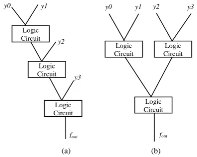
simultaneously but the carry bits must ripple from the least significant bit up to the most significant bit. The most significant bit of the adder could switch n times due to ripple factor. The sum is computed at the final transition. The other intermediary switching is analogous to glitch. For example, the carry-out of 32nd bit of a 32-bit ripple carry adder is switched 32 times and sum-out also switches 32 times before a final computation is made. The higher significant bits have larger switching rate. Figure 1 illustrates two types of logic circuits, glitch-prone and glitch-free circuits.
There are number of algorithms proposed to optimize the FPGA performance and speed of execution of underlying functions of algorithms. Versatile place and route software is quite often used for optimization of routing operations in FPGA [3]. The problem of glitches in FPGA was tried by mapping that balances LUT levels for different paths [4]. Yet another research aimed at reducing glitches by inserting programmable delay units into configurable logic blocks of FPGAs [5]. The delay units make sure that all signals arrives at the same time at LUT. Some of the recent research on this topic suggests that there have been efforts to reduce glitches targeted to FPGAs. The delay due to various interconnections is more responsible for glitches compared to logic functional delay.
[image:2.595.69.265.104.260.2]Many researchers have used versatile place and route (VPR) toolset for FPGA placement and routing with Pathfinder [5], [6]. CAD based designs have shown good results for minimization of glitches which reduces dynamic power up to 10% and more significantly these do not change architecture of the design [7]. A solution based on critical path with least delay used Lagrangian relaxation method [8]. In as far as algorithms are concerned, FPGA routing based on the congestion was proposed in the Pathfinder research [9]. Firstly, a small sub group of critical paths is identified and then the group is optimized by repeated trials of remaking group by including some more paths and simultaneously excluding other paths. There may be some of the paths overlapping and hence least delay path method may not be very efficient. More recent work for glitch minimization includes new tools that can be used to investigate the power consumption in FPGA circuits and architectures. [10], [11]. These methods are normally hybrid in the nature that the combination of techniques such as GlitchMap, GlitchLess etc. with efficient place and route algorithms often produce a better solution. This research had demonstrated through simulation tests that interconnects are usually the major power consumption sources in FPGA and thereby total interconnect power is dominant. Leakage power can also be considerable at nano-scales as the transistors are more likely to be suffering from leakage current at this scales. Area optimization in FPGA had also been studied in details and proposed details are supporting the fact that dynamic power can be, to some extent, minimized. These techniques are helpful in two ways as these tend to minimization of the dynamic power consumption and same time area on the chip [12], [13]. In one of the research, the shortest path technique is combined with other constraints [14] such as complexity, hazards and fault prone nodes of a graph. Here, the idea is that physically short path may not be always good enough to optimize dynamic power consumption in FPGAs. There are studies suggesting that the relation between Boolean operations and algebraic operations depends upon probabilities of each input being logical 0 or 1 [15]. The fault detection may be strongly depended upon these probabilities and thus determined power consumption should be a function of accuracy of fault detection. The switching activity and capacitance effects are Figure 1. Topology of logic circuits (a) Glitch prone
and (b) Glitch free
Logic Circuit
Logic Circuit
Logic Circuit
y0
(a)
y1
y2
y3
fout
y2
Logic Circuit
Logic Circuit
Logic Circuit
(b)
fout y1
depicted in figure 2. These variations show that as levels of the logic circuit, through which signals travel, increase, the capacitive effects and switching activities both increase. The rate of capacitance increase is faster and thus delays also increase accordingly.
3.
LOGIC DESIGN IMPLEMENTATION
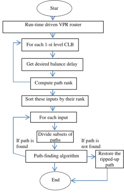
The general algorithm overview used for implementing carry select adder and booth multiplier is illustrated by figure 3. Firstly a VPR router is initialized and then balancing is done for chosen subsets of the paths with the goal of minimization of delay and cost function in terms of length. Selected pairs are reordered and then divided again in order to form new pairs. Next step consist of using path finding algorithms to reroute the paths with least delays and lengths of the paths in order to reduce overall delay [16], [17].
The inputs are selected based on the principle that a longer path would always result in power overheads due to more capacitance involved and a number of buffers that appear in the path of a signal as it travels through circuit levels. Balancing is only performed on the relevant and effective inputs as all inputs may not need balancing or may not actually cause glitches. The balancing is performed by using heuristic approach with constraints of switching activities and capacitance as illustrated in figure 2.
LUT inputs are required to be ordered for the likelihood of probable glitch occurrences. For ordering Boolean difference signal probability and binary decision diagrams are also cosidered as constraints. This research work focused on multiple existing algorithms for computing ordering arrangements. The experimental setup preferred small increase in delays rather than large delays for simulations tests. Then, finally the path ranking is determined for each path. Figure 3 illustrates the general arrangement of the experimental execution steps for glitch re-router algorithm for conducting simulation tests for two chosen circuits of carry select adder and booth multiplier chosen for experimental tests. The flow chart sequence shows step by step method to determine the path order, input signal balance and the ranks of the input signals. Firstly a small set of paths of finite length is chosen. Paths with smallest delays are identified and then combine all such paths. Again increase the delay and repeat the steps until a final threshold level is reached during iterations. The target paths are chosen by selecting nodes
closest in vicinity and ensuring that no overlaps occur when edges are connected.
For example, in a given data module, the experimental setup included 16 delay paths with different widths. The different widths of signals ensure that each of the 16 signals arrive at different times at LUT while travelling through chosen paths. On reaching to LUT, the signals get switched from 0 to 1 or 1
to 0. The mismatched arrival of signals at LUT leads to unnecessary power dissipation in the circuit. It can be avoided if design is planned and implemented properly on FPGAs.
The power so wasted can be minimized if some logic block in FPGAs can route the incoming signal on balanced paths at the time of signal reaching to router module. The router switches the received data on to a balanced path based on its time delay. Balancing path module balances the switched data. The balancing paths match time delay between data paths and LUT. The synchronization block within LUT receives data from balancing path and performs synchronization on 16 bit to check the received data for accuracy. In the next step it
separates a 16 bit data block and sends it to LUT Block. LUT
[image:3.595.334.535.125.439.2]stores the synchronized data which can be used for any combinational and sequential operations to be performed by the logic circuit in the future operations. The simple method explained here is very effective and easy to implement for validations and simulation tests. Though the method is not new and many researchers have applied for optimization, this
Figure 3. Flowchart for glitch minimization in logic design of carry select adder and booth multiplier circuits.
Star t
Run-time driven VPR router
For each 1-st level CLB
Get desired balance delay delay
Compute path rank
Sort these inputs by their rank
For each input
Divide subsets of paths
Path-finding algorithm Restore the ripped-up
path If path is
found
End
[image:3.595.58.274.134.292.2]If path is not found Figure 2. Switching Activity Vs Capacitance with increasing
paper describes elaborately for two new benchmarking circuits for simulations test.
4.
SIMULATION RESULTS
The experimental setup was based on a computer system with a 2.20 GHz Intel (R) Core (TM)2 Duo CPU with a system type of 32-bit operating system from Microsoft Inc. The
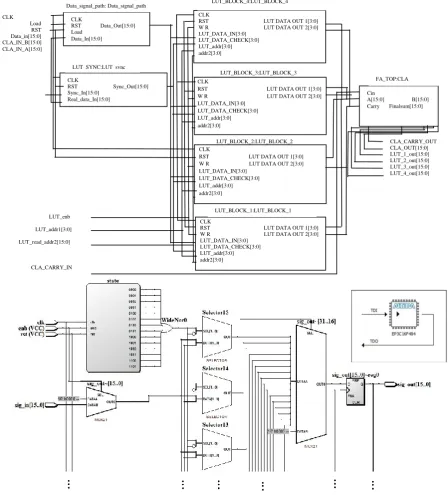
benchmarking circuits for carry select adder used are shown in figure 4 and figure 5 with glitch unaware and glitch aware implementation respectively. The comparison of algorithm, GlitchReroute, with glitch unaware versatile place and route’s router and glitch aware router is illustrated in figure 4 and
figure 5. The LUT input size was selected with k = 16. Main
implementation platform was EP3C16F484C6 Cyclone III device family from Altera Inc. as shown in figure 4 in box. The software platform used was Quartus-II for running simulation tests. Quartus version 10.1 Build 153 11/29/2010 SJ Web Edition, which is a registered trademark of Altera Corporation. The toolbox, PowerPlayAnalyzer, a part of Altera’s Quartus II software was used for estimating power
[image:4.595.64.513.169.665.2]consumption on FPGA implementation of carry select adder. The Quartus II was run for simulation in order to synthesize, place, and route the circuit of adders as mentioned above. These files are used for both glitch unaware versatile place and route’s router and glitch aware versatile place and route’s router for proposed circuit.
Figure 4. Glitch unaware-view of RTL schematic block diagram of carry select adder as a benchmarking circuit CLK
Load RST Data_in[15:0] CLA_IN_B[15:0] CLA_IN_A[15:0]
LUT_enb
LUT_addr1[3:0]
LUT_read_addr2[15:0]
CLA_CARRY_IN CLK
RST Data_Out[15:0] Load
Data_In[15:0]
Data_signal_path: Data_signal_path
CLK
RST Sync_Out[15:0] Sync_In[15:0]
Real_data_In[15:0] LUT_SYNC:LUT_sync
CLK
RST LUT DATA OUT 1[3:0] W R LUT DATA OUT 2[3:0] LUT_DATA_IN[3:0]
LUT_DATA_CHECK[3:0] LUT_addr[3:0] addr2[3:0] CLK
RST LUT DATA OUT 1[3:0] W R LUT DATA OUT 2[3:0] LUT_DATA_IN[3:0]
LUT_DATA_CHECK[3:0] LUT_addr[3:0] addr2[3:0]
LUT_BLOCK_4:LUT_BLOCK_4
LUT_BLOCK_1:LUT_BLOCK_1
Cin
A[15:0] B[15:0] Carry Finalsum[15:0]
FA_TOP:CLA
CLA_CARRY_OUT CLA_OUT[15:0] LUT_1_out[15:0] LUT_2_out[15:0] LUT_3_out[15:0] LUT_4_out[15:0] LUT_BLOCK_3:LUT_BLOCK_3
LUT_BLOCK_2:LUT_BLOCK_2 CLK
RST LUT DATA OUT 1[3:0] W R LUT DATA OUT 2[3:0] LUT_DATA_IN[3:0]
LUT_DATA_CHECK[3:0] LUT_addr[3:0] addr2[3:0]
CLK
RST LUT DATA OUT 1[3:0] W R LUT DATA OUT 2[3:0] LUT_DATA_IN[3:0]
Glitchreroute was performed on Quartus II to simulate the circuits and generate a Netlist viewer specifically for RTL schematics. Figure 4 also shows the routing module. Next step was to run PowerPlayAnalyzer to estimate the power consumption on board FPGA. For this a LUT of input size
k=16 was used. The PowerPlayAnalyzer reports showed
power estimation for carry select adder. Table 1 enlists the dynamic power consumption which was computed by using PowerPlayAnalyzer simulation test on carry select adder
[image:5.595.78.504.206.560.2]circuit. GlitchReroute is able to reduce dynamic power consumption by 11.5% compared to glitch unaware versatile place route’s router. The total power consumed has not been shown by each circuit due to the fact that LUTs that mapped circuits were much fewer than the total number of LUTs available in the Cyclone III devices. This means that most of the power is consumed by unused LUTs and thus the total power is not comparable to the used LUTs by algorithm with glitch unaware router fairly.
Table 1: Performance comparison analysis
Combinational logic
Routing Type
Total logic elements I/O
pins
Total Registers
Peak inter- connect
usage
Dynamic Power Dissipation
(mW)
Total combinational
functions
Dedicated logic register
No. of registers using
Synchronous Clear
No. of registers using Asynchronous
Clear
No. of registers using Clock
Enable
Carry Select Adder
Glitch unaware router
249 238 142 16 141 141 6% 77.31
Glitch aware router
192 96 46 16 0 16 2% 68.29
Booth Multiplier
Glitch un aware router
317 372 158 17 141 238 5% 78.81
Glitch aware router
262 246 78 17 0 17 4% 71.30
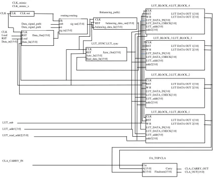
Figure 5. Glitch aware-view of RTL schematic block diagram of carry select adder as a benchmarking circuit
CLK CLK CLK out
CLK_mimic: CLK_mimic_x
CLK Load RST Data_in[15:0]
CLK
RST Data_Out[15:0] Load
Data_In[15:0] Data_signal_path: Data_signal_path
clk
enb sig out[15:0] rst
sig in[15:0] routing:routing
CLK
RST Sync_Out[15:0] Sync_In[15:0]
Real_data_In[15:0] LUT_SYNC:LUT_sync
LUT_enb
LUT_addr1[3:0]
LUT_read_addr2[15:0]
CLA_CARRY_IN
LUT_BLOCK_1:LUT_BLOCK_1 CLK
RST LUT DATA OUT 1[3:0] W R LUT DATA OUT 2[3:0] LUT_DATA_IN[3:0]
LUT_DATA_CHECK[3:0] LUT_addr[3:0] addr2[3:0]
LUT_BLOCK_4:LUT_BLOCK_4
Cin
A[15:0] Carry B[15:0] Finalsum[15:0]
FA_TOP:CLA
CLA_CARRY_OUT CLA_OUT[15:0] CLK
RST LUT DATA OUT 1[3:0] W R LUT DATA OUT 2[3:0] LUT_DATA_IN[3:0]
LUT_DATA_CHECK[3:0] LUT_addr[3:0] addr2[3:0]
CLK
RST LUT DATA OUT 1[3:0] W R LUT DATA OUT 2[3:0] LUT_DATA_IN[3:0]
LUT_DATA_CHECK[3:0] LUT_addr[3:0] addr2[3:0]
CLK
RST LUT DATA OUT 1[3:0] W R LUT DATA OUT 2[3:0] LUT_DATA_IN[3:0]
LUT_DATA_CHECK[3:0] LUT_addr[3:0] addr2[3:0]
LUT_BLOCK_2:LUT_BLOCK_2 LUT_BLOCK_3:LUT_BLOCK_3 CLK
RST balancing_data_out[15:0] balancing_data_In[15:0]
Generally, the carry-select adder consists of two ripple carry adders and a multiplexer. Two n-bit numbers are added by a carry-select adder by using two ripple carry adders. In order to perform the computation two times, two carry adder circuits are required, first time with the assumption that the carry being 0 and second time with assumption that the carry is
being 1. After accomplishment of two computations, the
results of correct sum, as well as the correct carry are determined.
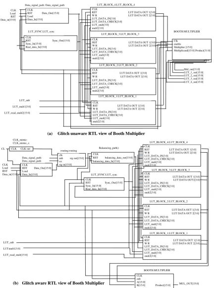
[image:6.595.84.517.76.658.2]The second benchmarking circuit chosen was booth multiplier. Booth’s multiplication algorithm multiplies two Figure 6. Glitch (a) unaware and (b) glitch aware RTL schematic block diagrams of booth multiplier as a
benchmarking circuit CLK
Load RST Data_in[15:0]
LUT_enb
LUT_mult1[3:0]
LUT_read_mult2[15:0] CLK
RST Data_Out[15:0] Load
Data_In[15:0]
Data_signal_path: Data_signal_path
CLK
RST Sync_Out[15:0] Sync_In[15:0]
Real_data_In[15:0] LUT_SYNC:LUT_sync
CLK
RST LUT DATA OUT 1[3:0] W R LUT DATA OUT 2[3:0] LUT_DATA_IN[3:0]
LUT_DATA_CHECK[3:0] LUT_mult[3:0] mult2[3:0] CLK
RST LUT DATA OUT 1[3:0] W R LUT DATA OUT 2[3:0] LUT_DATA_IN[3:0]
LUT_DATA_CHECK[3:0] LUT_mult[3:0] mult2[3:0]
LUT_BLOCK_4:LUT_BLOCK_4
LUT_BLOCK_1:LUT_BLOCK_1
Clk enable Multiplier [15:0] Multiplicand[15:0] Product[31:0] BOOTH:MULTIPLIER
Mul_out[31:0] LUT_1_out[15:0] LUT_2_out[15:0] LUT_3_out[15:0] LUT_4_out[15:0] LUT_BLOCK_3:LUT_BLOCK_3
LUT_BLOCK_2:LUT_BLOCK_2 CLK
RST LUT DATA OUT 1[3:0] W R LUT DATA OUT 2[3:0] LUT_DATA_IN[3:0]
LUT_DATA_CHECK[3:0] LUT_mult[3:0] mult2[3:0]
CLK
RST LUT DATA OUT 1[3:0] W R LUT DATA OUT 2[3:0] LUT_DATA_IN[3:0]
LUT_DATA_CHECK[3:0] LUT_mult[3:0] mult2[3:0]
CL K
CLK CLK out CLK_mimic: CLK_mimic_x
CLK Load RST Data_in[15:0]
CLK
RST Data_Out[15:0] Load
Data_In[15:0] Data_signal_path: Data_signal_path
clk
enb sig out[15:0] rst
sig in[15:0] routing:routing
CLK
RST Sync_Out[15:0] Sync_In[15:0]
Real_data_In[15:0] LUT_SYNC:LUT_sync
LUT_enb
LUTmult1[3:0]
LUT_read_mult[15:0]
LUT_BLOCK_1:LUT_BLOCK_1 CLK
RST LUT DATA OUT 1[3:0] W R LUT DATA OUT 2[3:0] LUT_DATA_IN[3:0]
LUT_DATA_CHECK[3:0] LUT_mult[3:0] mult2[3:0]
LUT_BLOCK_4:LUT_BLOCK_4
CLK enb
A[15:0] B[15:0] Product[15:0]
BOOTH:MULTIPLIER
MUL_OUT[15:0] CLK
RST LUT DATA OUT 1[3:0]
W R LUT DATA OUT2[3:0] LUT_DATA_IN[3:0]
LUT_DATA_CHECK[3:0] LUT_mult[3:0] mult2[3:0]
CLK
RST LUT DATA OUT 1[3:0] W R LUT DATA OUT 2[3:0] LUT_DATA_IN[3:0]
LUT_DATA_CHECK[3:0] LUT_mult[3:0] mult2[3:0]
CLK
RST LUT DATA OUT 1[3:0] W R LUT DATA OUT 2[3:0] LUT_DATA_IN[3:0]
LUT_DATA_CHECK[3:0] LUT_mult[3:0] mult2[3:0]
LUT_BLOCK_2:LUT_BLOCK_2 LUT_BLOCK_3:LUT_BLOCK_3 CLK
RST balancing_data_out[15:0] balancing_data_In[15:0]
Balaancing_path()
(a) Glitch unaware RTL view of Booth Multiplier
signed binary numbers in two’s complement notation. Booth used desk calculators for multiplication that were faster at shifting than adding. He invented an algorithm to increase the multiplication speed. Booth’s algorithm is quite often used by researcher of computer architecture and related topics.
Figure 6 shows the RTL view of booth’s multiplier for glitch unaware and glitch aware simulation results respectively. The power consumptions report is shown in Table 1. Similar to the carry select adder, the experimental set up consisted of a LUT
of input size k=16 for Booth’s multiplier. The
PowerPlayAnalyzer was used to generate power reports. For Booth’s multiplier, dynamic power consumption was reduced by a 7.5% compared to glitch unaware versatile place route’s router simulation.
5.
CONCLUSION
In this paper, the authors have presented a technique for reducing dynamic power in FPGAs by minimizing glitches during routing for two specific circuits of carry select adder and Booth’s multiplier. The routing was carried out with GlitchReroute routing approach. The algorithm tried to find routes with target delays and balancing paths leading to LUT inputs, so that signal arrival times are aligned at LUT. The simulation tests have shown a reduction in dynamic power consumption in FPGAs. Finally a comparison was made with glitch unaware versatile place and route’s router and glitch aware router. The results attained 11.5% reduction in dynamic power in FPGAs on implementation of carry select adder and a similarly a 7.5 % reduction in power consumption in case of Booth’s multiplier was observed.
For further research in the future, it is planned that dynamic power in FPGAs can still be reduced by using path balancing technique with other glitch reduction technique as a hybrid approach in FPGA. These approaches may include technology mapping and technology decomposition.
6.
REFERENCES
[1] Q. Dinh, D. Chen, and D. F. Wong, “A routing approach
to reduce glitches in low power FPGAs,” in Proc. of Int. Symp. Physical Design, 2009, pp. 99–106.
[2] Quang Dinh, Deming Chen and Martin D. F. Wong, “A
Routing Approach to Reduce Glitches in Low Power FPGAs”, IEEE Trans. on Computer-Aided Design of Integrated Circuits and Systems, Vol. 29, No. 2, 2010, pp 235-240.
[3] F. Li, D. Chen, L. He, and J. Cong, “Architecture
evaluation for power efficient FPGAs”, in Proc. Int. Symp. Field-Programmable Gate Arrays, 2003, pp. 175–184.
[4] L. Cheng, D. Chen, and D. F. Wong, “GlitchMap: An
FPGA technology mapper for low power considering glitches,” in Proc. Design Autom. Conf., 2007, pp. 318– 323.
[5] J. Lamoureux, G. Lemieux, and S. Wilton, “GlitchLess:
Dynamic power minimization in FPGAs through edge
alignment and glitch filtering,” IEEE Trans. Very Large Scale Integr. Syst., vol. 16, no. 11, pp. 1521–1534, Nov. 2008.
[6] V. Betz and J. Rose, “VPR: A new packing, placement
and routing tool for FPGA research,” in Proc. Int. Workshop Field Programmable Logic Applicat., 1997, pp. 213–222.
[7] V. Betz, J. Rose, and A. Marquardt, “Introduction,” in Architecture and CAD for Deep-Submicron FPGAs. Boston, MA: Kluwer Academic, 1999, pp. 1–10.
[8] S. Lee and M. D. F. Wong, “Timing-driven routing for
FPGAs based on Lagrangian relaxation,” IEEE Trans. Comput.-Aided Design Integr. Circuits Syst., vol. 22, no. 4, pp. 506–510, Apr. 2003.
[9] L. McMurchie and C. Ebeling, “PathFinder: A
negotiation-based performance-driven router for
FPGAs,” in Proc. Int. Symp. Field- Programmable Gate Arrays, 1995, pp. 111–117.
[10] F. Li, Y. Lin, L. He, D. Chen, and J. Cong, “Power modeling and characteristics of field programmable gate arrays,” IEEE Trans. Computer.-Aided Design Integr. Circuits Syst., vol. 24, no. 11, pp. 1712–1724, 2005.
[11] R. Fung, V. Betz, and W. Chow, “Simultaneous
short-path and long short-path timing optimization for FPGAs,” in Proc. Int. Conf. Comput.-Aided Design, 2004, pp. 838– 845.
[12] D. Chen and J. Cong, “DAOmap: A depth-optimal area
optimization mapping algorithm for FPGA designs,” in Proc. Int. Conf. Computer-Aided Design, 2004, pp. 752–759.
[13] B. Ramkumar and Harish M Kittur, “Low-Power and
Area-Efficient Carry Select Adder” in IEEE trans. On VLSI systems
[14] E. Dijkstra, “A note on two problems in connection with
graphs”, in Numer. Math., vol. 1, no. 1, pp. 269–271, Dec. 1959.
[15] K. P. Parker and E. J. McCluskey, “Probabilistic
treatment of general combinational networks,” IEEE Trans. Comput., vol. C-24, no. 6,pp. 668–670, Jun. 1975.
[16] A. Raghunathan, S. Dey, and N. K. Jha, “Register
transfer level power optimization with emphasis on glitch analysis and reduction,” IEEE Trans. Comput.-Aided Design Integr. Circuits Syst., vol. 18, no. 8,pp. 1114–1131, Aug. 1999.
[17] E. M. Sentovich, K. J. Singh, L. Lavagno, C. Moon, R.