University of Warwick institutional repository: http://go.warwick.ac.uk/wrap
This paper is made available online in accordance with publisher policies. Please scroll down to view the document itself. Please refer to the repository record for this item and our policy information available from the repository home page for further information.
To see the final version of this paper please visit the publisher’s website. Access to the published version may require a subscription.
Author(s): O.M. Alatise, K.S.K. Kwa, S.H. Olsen, A.G. O’Neill
Article Title: The impact of self-heating and SiGe strain-relaxed buffer thickness on the analog performance of strained Si nMOSFETs Year of publication: 2010
Link to published article:
http://dx.doi.org/10.1016/j.sse.2009.09.029
Publisher statement: “NOTICE: this is the author’s version of a work that was accepted for publication in Solid-State Electronics resulting from the publishing process, such as peer review, editing, corrections, structural formatting, and other quality control mechanisms may not be reflected in this document. Changes may have been made to this work since it was submitted for publication. A definitive version was
The Impact of Self-Heating and SiGe Strain Relaxed Buffer
Thickness on the Analog Performance of Strained Si nMOSFETs
O. M. Alatise, K.S.K. Kwa, S.H. Olsen and A.G. O’Neill,
School of Electrical, Electronic and Computer Engineering, Newcastle University,
Newcastle upon Tyne, NE1 7RU, UK
School of Electrical, Electronic and Computer Engineering,
Newcastle University
Merz Court, Newcastle upon Tyne, NE1 7RU, UK
E-mail: [email protected]
Tel: +44-(0)191-222-7595
Abstract- The impact of the SiGe strain relaxed buffer (SRB) thickness on the analog
performance of strained Si nMOSFETs is investigated. The negative drain conductance
caused by self-heating at high power levels leads to negative self-gain which can cause
anomalous circuit behavior like non-linear phase shifts. Using ac and dc measurements,
it is shown that reducing the SRB thickness improves the analog design space and
performance by minimizing self-heating. The range of terminal voltages that leverage
positive self-gain in 0.1 µm strained Si MOSFETs fabricated on 425 nm SiGe SRBs is
increased by over 100% compared with strained Si devices fabricated on conventional
SiGe SRBs 4 µm thick. Strained Si nMOSFETs fabricated on thin SiGe SRBs also show
45% improvement in the self-gain compared with the Si control as well as 25%
enhancement in the on-state performance compared with the strained Si nMOSFETs on
the 4 µm SiGe SRB. The extracted thermal resistance is 50% lower in the strained Si
device on the thin SiGe SRB corresponding to a 30% reduction in the temperature rise
compared with the device fabricated on the 4 µm SiGe SRB. Comparisons between the
maximum drain voltage for positive self-gain in the strained Si devices and the ITRS
projections of supply voltage scaling show that reducing the SiGe SRB thickness would
be necessary for future technology nodes.
Index Terms- Analog MOSFET, Self-heating, Silicon-Germanium, Strained Silicon,
I. INTRODUCTION
Tensile strained silicon (Si) enhances electron mobility by lifting the conduction
band degeneracies, reducing carrier scattering and increasing the population of carriers in
sub-bands with lower transverse effective mass [1]. Strained Si implemented in radio
frequency complimentary metal oxide on semiconductor (RFCMOS) shows good prospects
for mixed signal solutions. The epitaxial deposition of Si on silicon-germanium strain relaxed
buffers (SiGe SRBs) generates biaxial tensile strain in the Si layer with a strain magnitude
that is proportional to the degree of lattice mismatch. Manufacturing difficulties such as the
production cost of graded buffers, process optimization, silicidation chemistry, yield and
device issues such as germanium (Ge) out diffusion, oxide interface properties and
self-heating, have made uniaxial (or process induced) strain preferable to biaxial strain.
Uniaxial strain induced by silicon nitride (Si3N4) contact etch stop layers and source/drain
silicon-germanium (SiGe) selective epitaxial growth have made inroads into industrial CMOS
processes [2, 3]. The stress magnitude predicted by simulations of such devices is as high as
600 MPa [4]. This is less than what is obtainable on biaxial strained substrates, where stress
magnitudes in excess of 1.4 GPa can be realised, corresponding to strained Si epitaxially
grown on a Si0.8Ge0.2 SRB. Since much larger values of strain can be realized, it is worthwhile
to investigate some of the challenges that arise from strained layer heteroepitaxy. This
investigation addresses one such challenge, namely, self-heating and its impact on analog
metal oxide on semiconductor field effect transistor (MOSFET) performance.
Self-heating arises from the lower thermal conductivity of SiGe relative to Si, which
means that the MOSFET is less capable of dissipating heat as the channel current is increased
since the channel is separated from the substrate by a low thermal conductivity SRB layer [5,
6]. The consequence is increased carrier scattering that lowers the drain current in saturation
where the power levels are higher. Self-heating is important in analog devices where the duty
cycle is higher (the MOSFET is on for longer periods of time) and the drain conductance
behaviour of the MOSFET is important because of its relationship with the output resistance
and self-gain. Self-heating is most observable in the MOSFET output characteristics where
the reduction in the drain current from its saturation magnitude is obvious as the drain voltage
is increased. This amounts to a negative drain conductance which causes a negative self-gain
and thus renders the circuit behaviour anomalous by causing non-linear operation and phase
shift [7]. Simulations of the frequency response of high gain amplifiers using bipolar junction
transistors showed that self-heating can cause serious errors in the small signal parameters
and affect the compensation of such circuits [8]. Self-heating was reported to exacerbate
current mismatch due to localized temperature differences which affect the performance of
circuits such as current mirrors and digital-to-analog converters that strongly depend on
current matching [9]. It was also shown that small signal amplifier characteristics displayed
visible anomalies due to self-heating. Hence, circuit designers using strained Si technology on
SiGe SRBs must be careful to ensure that the bias terminals of the MOSFET are such that the
drain conductance is not negative. This implies limitations in the range of gate and drain
voltages caused by the possibility of negative drain conductance.
Thin SiGe SRBs have been proposed as a method of reducing self-heating in strained
Si MOSFETs [10, 11]. Conventional graded buffers have thicknesses that are normally on the
order of one or several micrometers thick however literature shows that progress has been
made on the reduction of buffer thicknesses. Some studies on thin SiGe SRB technology
focus on materials growth and characterization [12-14] whereas others focus on self-heating
in devices [10, 11, 15-21]. The introduction of point defects during the growth of the SRB has
been demonstrated as a method of fabricating thin SiGe SRBs [13]. Si0.6Ge0.4 SRBs with
point defect supersaturation at low growth temperatures [14]. Thicknesses below 100 nm
were achieved for SiGe SRBs with Ge percentages as high as 70% [13]. 500 nm thick
Si0.56Ge0.44 SRBs prepared by low energy plasma enhanced chemical vapour deposition
(PECVD) with acceptable defect density magnitudes were reported but were used in
fabricating modulation doped field effect transistors (MODFETs) [20]. Olsen et al used 200
nm SiGe SRBs to demonstrate that some of the performance enhancement lost to self-heating
at high terminal voltages in thick SRB devices can be recovered by scaling the buffer
thickness [10]. Strained Si pMOSFETs on a 400 nm Si0.8Ge0.2 SRB were demonstrated by Lei
et al [18] with on-state enhancements of 25%. Sawano et al achieved 100 nm SRB thickness
with 17% Ge content and full relaxation using ion implantation [21].
There has been no reported investigation on the impact of SiGe SRB scaling on the
analog performance of strained Si MOSFETs. This investigation for the first time shows the
impact of self-heating on the analog performance of strained Si MOSFETs and how thin SiGe
SRBs can be used to limit the deleterious nature of self-heating by relaxing the limitations
imposed on the design space.
II. DEVICE FABRICATION
A Si control wafer, a wafer with strained Si grown on a conventional thick SiGe SRB
and a wafer with strained Si on a thin SiGe SRB were co-processed. The device on the thick 4
µm SiGe SRB comprised a 2.5 µm graded buffer, a 1.5 µm constant composition Si0.8Ge0.2
layer and a 10 nm tensile strained Si layer. In the case of the thin SiGe SRB devices, a layer
of SiGe:C was used to achieve high strain relaxation. The total thickness in the thin SRB was
425 nm. The MOSFETs underwent an identical MOSFET process fabrication flow. A 1.4 nm
gate oxide was thermally grown followed by 100 nm pre-doped poly deposition. Next was
sidewall spacer formation, source/drain deep implants, nickel silicidation and aluminum
metallization. A variety of gate lengths were fabricated with 10 µm gate widths. Fig. 1 shows
the cross-sectional TEM of the thin and thick SiGe strain relaxed.
III. ELECTRICAL RESULTS AND DISCUSSION
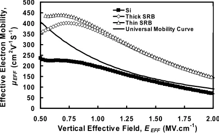
Using the split CV technique with series resistance correction [22], the effective
mobility was extracted from 1 µm gate length devices. Fig. 2 shows the effective electron
mobility as a function of the vertical effective field. The thin and thick SRB devices both
exhibited 100% mobility enhancement compared with the Si control device. This result shows
that the effective strain in the thin and thick SiGe SRB devices is equivalent and that buffer
scaling has not adversely affected mobility enhancement.
A model was developed in [23] for small signal output admittance parameters in
silicon-on-insulator (SOI) MOSFETs and was used to show the non-linear behaviour of
CMOS inverters and cascode amplifiers with self-heating taken into account [7]. Using this
model, the DC self-gain of the MOSFET can be expressed as
DS TH DS
m V
I R g
g A
θ
+
= (1)
where AV is the self-gain, gm is the transconductance, gDS is the drain conductance, RTH is the
thermal resistance, θ is the temperature sensitivity of the mobility and IDS is the drain current.
From equation (1), it is apparent that a high RTH will have a negative impact on the AV of the
MOSFET. Due to the lower thermal conductivity of SiGe, the thermal resistance of SiGe
buffers is higher than that of Si and increases with the buffer thickness. Fig. 3 (a) and Fig.
gate length Si control nMOSFET and the strained Si nMOSFETs on the thin and thick SiGe
SRBs. Since future deep submicrometer technology nodes (0.022 µm and below) will have
non-minimum length (NML) analog MOSFETs with gate lengths of about 0.1 µm designed
for delivering high AV, the results in Fig. 3(b) are representative of state-of-the-art devices and
show that self-heating is an important factor in NML MOSFETs. It can be seen in Fig. 3(a)
that the 1 µm gate length strained Si nMOSFETs have significant self-gain enhancement
compared with the Si control device for VDS less than 1 V. At VDS= 0.5 V, the self-gain of the
strained Si nMOSFETs is an order of magnitude higher than the Si control device. As VDS is
increased, the percentage enhancement in the self-gain is reduced particularly for the strained
Si nMOSFET on the thick SiGe SRB where the self-gain becomes higher in Si. The reduction
in the self-gain at high VDS is due to self-heating and it can be seen from Fig. 3(a) that the
effect is ameliorated in the strained Si nMOSFET on the thin SiGe SRB. The problem of
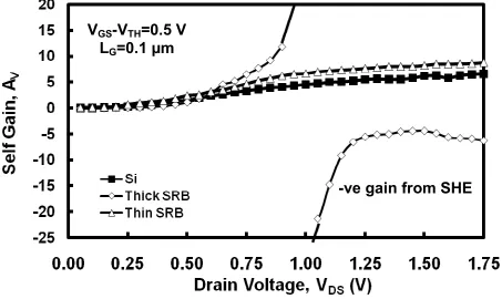
negative self-gain is however not exhibited for the 1 µm gate length devices. Fig. 3(b) shows
the same AV vs. VDS characteristics for the 0.1 µm gate length devices where a discontinuity
can be observed in the characteristic of the thick SiGe SRB device at a VDS of approximately 1
V. This discontinuity occurs when the denominator in (1) crosses the zero mark and the
self-gain rises infinitely. It can be seen from Fig. 3(b) that the problem of the negative
self-gain evident in the strained Si nMOSFETs on the thick SiGe SRB is eliminated in the thin
SiGe SRB. In addition, the self-gain of the strained Si nMOSFETs on the thin SiGe SRB also
shows up to 45% improvement compared with the bulk Si nMOSFET. The self-gain
improvement in the strained Si nMOSFET on the thin SiGe SRB evident in Fig. 3 is due to
improved on-state performance (higher gm) while maintaining similar drain conductance
(gDS).
The problem of negative self-gain due to self-heating in the strained Si nMOSFET on
(VGS & VDS) useable in analog circuits designed for high gain. To best illustrate the impact of
the buffer thicknesses on the design space, two-dimensional contour plots are used as shown
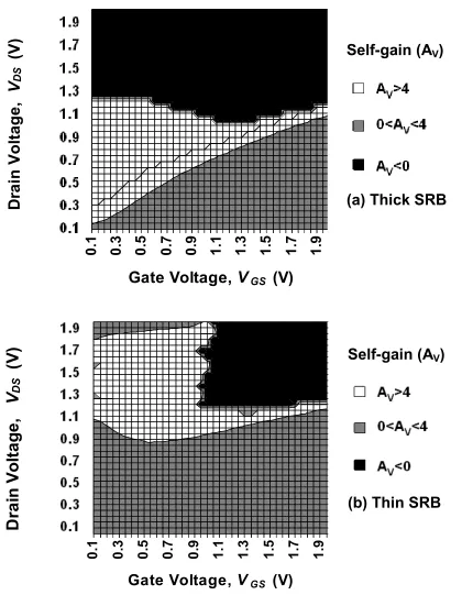
in Fig. 4a and Fig. 4b. Fig. 4a and Fig. 4b show the self-gain contours as functions of the VGS
and VDS for the 0.1 µm strained Si nMOSFETs on the thick and thin SRB respectively. In Fig
4a, approximately 40% of the design space area is comprised of negative self-gain, which
imposes very rigid limitations on the bias potentials available for delivering positive self-gain.
Drain voltages above 1.1 V for all gate voltages yield negative self-gain with the strain Si
nMOSFETs on the thick SiGe SRB. In Fig. 4b, the percentage area of the design space
comprised of negative self-gain is reduced to 15% because the potentials that cause negative
drain conductance are higher in magnitude thereby demonstrating the effectiveness of thin
SiGe SRBs in reducing the impact of self-heating. Hence, reducing the buffer thickness from
4 µm to 425 nm reduces the percentage area of negative self-gain on the contour maps from
40% to 15%. These plots indicate that the use of thin SiGe SRBs relax the restrictions that
self-heating imposes on the design space if normal analog circuit operation is to be ensured.
Self-heating also has a deleterious impact on the cut-off frequency of the device
which is another important analog metric. The cut-off frequency of the MOSFET is
proportional to the drain current and the transconductance. The performance enhancement in
the drain current of the strained Si device, which is reduced by self-heating at higher power
densities, can be recovered by thinning the SiGe buffer. The performance enhancement is
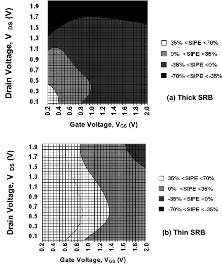
dependent on the terminal voltages of the MOSFET since the self-heating is a function of the
power levels. Fig. 5a shows the contour map of the performance enhancement in the 0.1 µm
gate length strained Si device on the thick SiGe SRB compared with the Si control whereas
Fig. 5b shows that of the strained Si nMOSFET on the thin SiGe SRB. Fig. 5a and Fig. 5b
show that the area with performance enhancement is approximately 25% and 90% for the
nMOSFET on the thick SiGe SRB, performance enhancement is evident only for small gate
overdrives and drain voltages because of self-heating at high power levels. This shows that
much of the performance enhancement lost to self-heating in the strained Si devices on the
thick SRBs is recovered in the strained Si devices on the thin SRBs. This is important for high
speed analog devices where the mobility enhancement due to strain can be manifested as
higher cut-off and maximum oscillation frequencies.
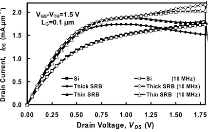
AC conductance measurements have been performed on the strained Si devices so as
to remove the effects of self-heating and extract the intrinsic device characteristics [24, 25].
The thermal resistance is also extracted from these measurements. The output characteristics
derived from the AC conductance technique is shown in Fig. 6 where the reduction in the
drain current characteristics due to self-heating has been removed by the high frequency
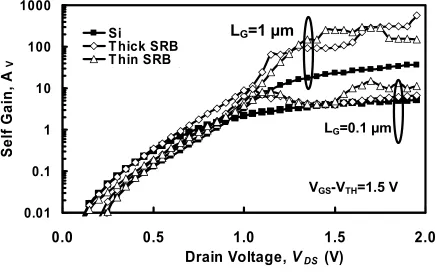
measurements. Fig. 7 shows the self-gain for 0.1 µm and 1 µm gate length nMOSFETs using
the high frequency (10 MHz) drain conductance measurements. Negative self-gain is absent
in the 0.1 µm gate length strained Si nMOSFET on the thick SiGe SRB and the intrinsic
performance of the device shows that the self-gain compared with Si control is improved by
mobility enhancement due to strain. Since the device under real circuit operation will not be
biased with a high frequency AC drain signal, the high frequency measurements of Fig. 6 and
Fig. 7 show the potential performance if the challenge of self-heating is solved.
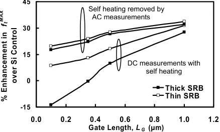
The impact of self-heating on the cut-off frequency is also ascertained by measuring
the maximum cut-off frequencies, ftMAX, of the devices at DC and at 10 MHz at a drain voltage
of 2 V. Fig. 8 shows the percentage enhancements in ftMAX for the strained Si devices on the
thick and thin SiGe SRBs as functions of the gate length with and without self-heating. The
percentage enhancement of ftMAX compared with the Si control extracted with self-heating
present reduces from 30% at 1 µm to -15% at 0.1 µm in the thick SRB device and from 30%
as the gate length is reduced. By reducing the thickness of the SiGe SRB from 4 µm to 425
nm, 25% of the ftMAX enhancement lost to self-heating at 0.1 µm gate length is recovered
thereby demonstrating the effectiveness of thinning the SiGe buffer. In the absence of
self-heating, Fig. 8 shows that the percentage enhancement of ftMAX reduces from 30% at 1 µm
to approximately 20% at 0.1 µm for both devices. Since 10% of the ftMAX enhancement is still
lost with self-heating removed, other factors such as series resistance and mobility
degradation (due to the higher channel doping in the strained Si devices) may be present.
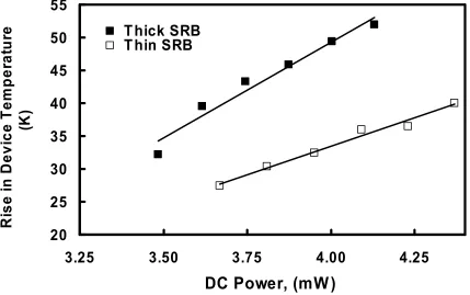
The thermal resistance is a measure of the heat conduction efficiency and can be used
to evaluate the amount of self-heating in the respective devices. The thermal resistances of the
strained Si devices have been calculated using (2) below which is a semi-empirical MOSFET
model with the temperature dependencies of the threshold voltage and effective mobility
taken into account. It was first derived for SOI MOSFETs in [25] and later used for strained
Si MOSFETs on SiGe SRBs in [11, 26].
( ) ( ) − + + − − + + + − + = − T k T T V LE V I T kI LE V T T V V I g V T T g g DSAT SAT DSAT DS DS SAT DSAT k O DS DSAT O DS DS DS O DST DS 600 exp 8 . 0 1 600 600 exp 8 . 0 1 1
1 β χ λ (2)
where gDS is the drain conductance at low frequencies, gDST is the drain conductance at
high frequencies, TO is the ambient temperature, T is the device temperature, VDSAT is the
saturation drain voltage, λ is the channel length modulation factor, L is the MOSFET gate
length, ESAT is the critical electric field, χ is the temperature threshold coefficient, k is
the mobility temperature exponent,
β
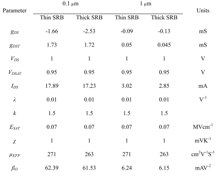
O is the transconductance factor and VDS is the drain(2) using measured values of the MOSFET parameters shown in table 1. The calculated
temperatures are shown as functions of the DC power, which is calculated as IDS.VDS for the
0.1 µm gate length strained Si nMOSFETs. Fig. 9 shows the rise in the device temperature as
a function of the DC power level where the higher temperatures are evident in the strained Si
nMOSFETs on the thick SiGe SRB. It is also observed that reducing the thickness of the SiGe
SRB from 4 µm to 425 nm reduces the temperature rise in the device by 30% which is
responsible for higher drive current and higher self-gain in the thin SiGe SRB device. The
thermal resistance, which is calculated as
(
T −TO)(
VDSIDS)
−1, is extracted from the slope of theline of best fit in Fig. 9. The thermal resistances of the 0.1 µm gate length strained Si
nMOSFETs on the thick and thin SiGe SRB were 30.5 K.mW-1 and 16.6 K.mW-1 respectively.
This amounts to approximately 50% reduction of the thermal resistance in the strained Si
device on the thin SiGe SRB.
Due to the fact that heat dissipation in strained Si nMOSFETs is not only dependent
on the thickness of the SiGe SRB, it is difficult to make comparisons of thermal resistances
between devices that are not co-fabricated. The gate length has an impact on the thermal
resistance. The thermal resistance is known to increase as the gate length is reduced because
the smaller cross-sectional area of the MOSFET reduces the heat conduction efficiency to the
Si substrate [27]. The strained layer thickness also affects the thermal resistance since the
typical strained Si thickness is much lower than the room temperature phonon mean free path
(200 nm to 300 nm at 300 K in Si) and phonon scattering at the Si/SiGe heterointerface will
contribute to the thermal resistance [27]. Other parameters such as the source/drain extension
and the sidewall spacer width will also affect the thermal resistance. The thermal resistance
values calculated here are comparable to what has been published in literature for strained Si
MOSFETs on SiGe SRBs [10, 26]. This reduction in thermal resistance and temperature rise
globally strained Si devices are to be implemented in mixed-signal applications.
Knowing the maximum drain voltage (VDSMAX) allowable for positive self-gain at a
particular gate length and SiGe buffer thickness is important for mixed signal design in
strained Si technology due to the fact that there are limits to how much SiGe buffers can be
scaled. The onset of negative gDS was at VDS =1.0 V and 1.25 V for the 100 nm LG strained Si
nMOSFET on the thick and thin SiGe SRB respectively. Hence, there is a fundamental
trade-off between VDSMAX and the maximum buffer thickness for positive self-gain. i.e. VDSMAX
decreases for thicker SiGe SRBs and increases for thinner SiGe SRBs. Since there are
challenges in scaling SiGe SRB thicknesses due to strain relaxation and threading dislocation
density requirements, circuit designers can scale VDS as an alternative so as to ease the burden
on the device fabricators. However, there are also limits to VDS scaling and other design
parameters may affect the choice of the drain bias. The choice of VDS depends on the
application. For example, laterally diffused power MOSFETs comprising of low doped drain
extensions are typically used for high power amplification in telecommunications base
stations. These devices are usually biased at drain voltages of about 28 V [28]. The gate
length of the device will also affect VDSMAX. VDSMAX reduces with the gate length which is
expected since the power density, hence self-heating increases with gate length reduction. Fig.
10 shows the drain conductance as a function of the drain voltage for 1 µm, 0.5 µm, 0.35 µm
and 0.1 µm gate length strained Si nMOSFETs on the thick SiGe SRBs at a gate voltage
overdrive of 1.5 V. At the inset of the Fig. 10 is a magnified illustration of how VDSMAX is
read-off from the drain voltage axis by taking the VDS point at which gDS=0. As the gate length
of the MOSFET is reduced from 1 µm to 0.1 µm, VDSMAX reduces from 1.2 V to 0.9 V, which
illustrates that fact that the design space becomes more rigid as for short channel MOSFETs.
There is already a long-term expectation in the semiconductor industry for scaling
in highly scaled analog MOSFETs as VDS may be reduced below VDSMAX. Scaling VDD is
essential in CMOS because the high lateral electric field caused by aggressive gate length
scaling has a negative impact on device reliability and also because of the rapidly increasing
power density in very large scale integration applications [30]. Power supply scaling is even
more important in some mixed signal wireless circuits where battery life is critical. However,
since VDD is not being scaled as aggressively as the MOSFET gate length, the problem of
self-heating still persists for now. The international technology roadmap for semiconductors
(ITRS) “RF and analog/mixed signal” guide [28] as well as the “Process Integration, Devices
and Structures” guide [29] is used to show the interplay between projected power supply
voltages and VDSMAX in strained Si MOSFETs at various gate lengths. Fig. 11 shows the
supply voltage as a function of the gate length for ITRS long and near term projections in low
standby power, high performance logic, high-speed NFET and low noise amplifier (LNA)
nFET. Fig 11 also shows that the VDSMAX of the strained Si nMOSFETs on the thin and thick
SiGe SRB. The devices on the thin SiGe SRB show greater flexibility in the design space
since VDSMAX is higher compared with the devices on the thick SRB for all gate lengths.
VDSMAX is improved by 30% for all the gate lengths in the strained Si nMOSFETs on the 425
nm thick SiGe SRB compared with the strained Si devices on the 4 µm thick SiGe SRB. Fig.
11 shows that SRB thinning is necessary for analog MOSFETs implemented in strained Si
since the VDD scaling has not gone below VDSMAX.
Scaling the power supply voltages has implications on the processing speed of
CMOS circuits. As the drain voltage is reduced, the lateral electric field is reduced and hence,
the velocity of the electrons entering the drain is also reduced. Higher drain voltages therefore
translate to shorter gate delay however, at the cost of higher power dissipation and
self-heating. This trade-off between the on-state speed and the power dissipation is well
power supply scaling, the importance of high mobility channels becomes more apparent as
technologists seek to maintain circuit speed at reduced power supplies. The low VDS
performance of the Si control and strained Si devices under investigation is assessed by
calculating the minimum gate delay as a function of VDS. The minimum gate delay, tDMIN, is
calculated from the maximum transconductance, gmMAX, extracted from the gate transfer
characteristics (IDS vs. VGS) by
MAX m
OX MIN
D
g
C
t
=
2
π
(3)
where COX is the gate dielectric capacitance per unit area. The percentage improvement in
tDMIN for the strained Si nMOSFETs on the thick and thin SiGe SRB is calculated. The results
of the calculations are shown in Fig. 12 where the percentage improvements in tDMIN
compared with the Si control are shown for the 0.1 µm gate length strained Si nMOSFETs as
functions of the drain voltage. It can be seen from Fig. 12 that the improvement in tDMIN
remains positive for the strained Si device on the thick and thin SiGe SRB up to 0.5 V and 0.8
V respectively. The performance reduction at high drain voltages is due to self-heating and
does not occur for longer gate length devices where power densities are lower. That
performance reduction occurs at a higher drain voltage for the thin SiGe SRB is indicative of
the fact that self-heating is reduced in the device by virtue of lower thermal resistance. Fig. 12
shows that the improvements in the on-state performance increases as the drain voltage is
reduced and is 15% higher for the strained Si nMOSFET on the thin SiGe SRB at VDS=0.5 V.
This is encouraging since Fig. 11 shows VDD could be scaled to 0.5 V in the near future.
Hence, the reduction in on-state performance from VDS scaling is replenished by the
projection of supply-voltage scaling is promising for the prospects of strained Si nMOSFETs
on thin SiGe SRBs since higher performance enhancement compared with the Si control is
obtainable at lower VDS. As VDD is scaled below VDSMAX, which is 30% higher for the thin
SiGe SRB, the problem of negative self-gain is diminished and better on state performance
enhancement is obtained.
IV. CONCLUSIONS
Analog circuit designers using strained Si/SiGe technology must be careful not to
bias MOSFETs in the design space of negative drain conductance otherwise the circuit may
produce negative gain and anomalous non-linear phase shift. It has been shown that reducing
the thickness of the SiGe SRB improves the design space of analog MOSFETs by reducing
the impact of self-heating. Measured data shows that the drain conductance in 425 nm thick
SiGe SRB devices is improved by 40% compared to the 4 µm thick SiGe SRB devices. A
45% improvement in self-gain compared with bulk Si was also obtained using thin SiGe
SRBs. AC conductance measurements were used to extract the thermal resistance of the
strained Si devices which was 50% lower in the strained Si nMOSFETs on the 425 nm thick
SiGe SRB where the temperature rise in the device was reduced by 30% compared with the
strained Si nMOSFETs on the 4 µm thick SiGe SRB. The intrinsic drain current was used to
compute the true self-gain of the MOSFETs, which showed over 100% enhancement in the
strained Si nMOSFETs. Measured data shows that thinner buffers are required to mitigate
self-heating in short channel devices and the maximum drain voltage for positive self-gain is
improved by 30% in the strained Si devices on the 425 nm thick SiGe SRB compared with the
4 µm thick SiGe SRB. Since there are limits to how thin SiGe SRBs can be and how small the
drain voltage can be scaled, the application requirements will determine which parameter will
V. ACKNOWLEDGEMENT
We would like to acknowledge the contribution of EUFP7 NANOSIL, EUFP6 SiNANO,
REFERENCES
[1] K. Rim, J. Hoyt, and J. Gibbons, "Analysis and fabrication deep submicron strained Si n-MOSFETs,"
IEEE Trans. Electron Devices, vol. 47, pp. 1406-1415, 2000.
[2] S. Thompson, G. Sun, Y. Choi, and T. Nishida, "Uniaxial process induced Strained Si: Extending the CMOS roadmap," IEEE Trans. Electron Devices, vol. 53, pp. 1010-1020, 2006.
[3] S. Thompson, "A Logic technology featuring strained Silicon," IEEE Electron Device Lett, vol. 25, pp. 191-193, 2004.
[4] S. Thompson, "A 90 nm logic technology featuring strained silicon," IEEE Trans. Electron Devices, vol. 51, pp. 1790-1797, 2004.
[5] G Nicholas, T Grasby, E Parker, T Whall, and T. Stotnicki, "Evidence of reduced self heating in strained Si MOSFETs," IEEE Electron Device Lett., vol. 26, pp. 684-686, 2005.
[6] K Rim, J Hoyt, and J. Gibbons, "Transconductance enhancement in deep submicron strained Si nMOSFETs," in IEDM Tech. Dig., pp. 707-710, 1998.
[7] M Fox and S. Brodsky, "Effects of self heating induced negative output conductance in SOI circuits,"
Proceedings in SOI Conference, pp. 152-153, 1993.
[8] R Fox, S Lee, and D. Zweidinger, "The effects of BJT self heating on circuit behavior," IEEE J. of
Solid-State Circuits, vol. 28, pp. 678-685, 1993.
[9] B. Tenbroek, M. Lee, W. White, J. Bunyan, and M. Uren, "Impact of self heating and thermal coupling on analog circuits in SOI CMOS," J. Solid-State Circuits., vol. 33, pp. 1037-1046, 1998.
[10] S Olsen, E Cousin, J Varzgar, R Agaiby, J Seger, P Dobrosz, S Chattopadhyay, S Bull, A O'Neill, P Hellstrom, J Edholm, M Ostling, K Lyutovich, M Oehme, and E. Kasper., "Control of self heating in thin virtual substrate strained Si MOSFETs," IEEE Trans. Electron Devices, vol. 53, pp. 2296-2305, 2006.
[11] R Agaiby, A O'Neill, S. Olsen, G. Eneman, P Verheyen, R Loo, and C. Claeys, "Quantifying self heating effects in strained Si MOSFETs with scaling," in Proc. ESSDERC, pp. 97-100, 2006.
[12] K. Lyutovich, M. Bauer, E. Kasper, H. Herzog, T. Perova, R. Maurice, C. Hofer, and C. Teichert, "Thin SiGe buffers with high Ge content for nMOSFETs," Mater. Sci. Eng. B, vol. 89, pp. 341-345, 2002. [13] K. Lyutovich, E. Kasper, F. Ernst, M. Bauer, and M. Oehme, "Relaxed SiGe buffer layer growth with
point defect injection," Mater. Sci. Eng. B, vol. 71, pp. 14-19, 2000.
[14] K. Lyutovich, J. Werner, M. Oehme, E. Kasper, and T. Perova, "Characterisation of virtual substrates with ultra-thin Si0.6Ge0.4 strain relaxed buffers," Mat. Sci. Semicond. Proc., vol. 8, pp. 149-153, 2005.
[15] H. Herzog, T. Hackbarth, U. Seiler, U. Konig, M. Luysberg, B. Hollander, and S. Mantl, "Si/SiGe nMODFETs on thin SiGe virtual substrates prepared by means of He implantation," IEEE Electron
Device Lett., vol. 23, pp. 485-487, 2002.
[16] T. Hackbarth, H. Herzog, F. Rinaldi, T. Soares, B. Hollander, S. Mantl, M. Luysberg, and P. Fichtner, "High frequency n-type MODFETs on ultra-thin virtual SiGe substrates," Solid-State Electron., vol. 47, pp. 1179-1182, 2003.
[17] T. Hackbarth, H. Herzog, K. Hieber, U. Konig, S. Mantl, B. Hollander, S. Lenk, H. Kanel, M. Enciso, F. Aniel, and L. Giguerrer, "Strained silicon FETs on thin SiGe virtual substrates produced by He
implantation: effect of reduced self heating on DC and RF performance," Solid-State Electron., vol. 48, pp. 1921-1925, 2004.
[18] M. Lei, Y. Hua, L. Chun, Y. Qi, Z. Jing, X. Jing, and T. Zhou, "Fabrication of strained Si channel pMOSFET on thin relaxed Si1-xGex virtual substrate," Proc. 7th International Conference on Solid State
and Integrated Circuits Technology, vol. 1, pp. 325-327, 2004.
[19] R. Agaiby, Y. Yang, S. H. Olsen, A. G. O'Neill, G. Eneman, P. Verheyen, R. Loo, and C. Claeys, "Quantifying Self-Heating Effects with Scaling in Globally Strained Si MOSFETs," Solid-State
Electron., vol. 51, pp. 1473-1478, 2007.
[20] T Hackbarth, H Herzog, K Hieber, U Konig, M Bollani, D Chrastina, and H. Kanel, "Reduced self heating in Si/SiGe field effect transistors on thin virtual substrates prepared by low energy plasma enhanced chemical vapour depostion," Appl. Phys. Lett., vol. 83, pp. 5465-5466, 2003.
[21] K Sawano, A Fukumoto, Y Hoshi, Y Shiraki, J Yamanaka, and K. Nakagawa, "Strained Si n channel metal oxide semiconductor field effect transistors formed on very thin SiGe relaxed layer fabricated by ion implantation technique," Appl. Phys. Lett., vol. 90, pp. 90-92, 2007.
[22] D. Schroeder, "Semiconductor material and device characterization," Wiley, 1998.
[23] A. Caviglia and A. Iliadis, "Linear dynamic self heating in SOI MOSFETs," IEEE Electron Device Lett., vol. 14, pp. 133-135, 1993.
significance for circuit simulation," IEEE Trans. Electron Devices, vol. 48, pp. 730-736, 2001.
[25] B Tenbroek, M Lee, W White, J Bunyan, and M. Uren, "Self heating effects in SOI MOSFETs and their measurement by small signal conductance technique," IEEE Trans. Electron Devices, vol. 43, pp. 2240-2248, 1996.
[26] K Jenkin and K. Rim, "Measurement of the effect of self heating in strained silicon MOSFETs," IEEE
Electron Device Lett., vol. 23, pp. 360-362, 2002.
[27] C. Fiegna, Y. Yang, E. Sangiorgi, and A. O'Neill, "Analysis of self heating effects in ultrathin-body SOI MOSFETs by device simulation," IEEE Trans. Electron Devices, vol. 55, pp. 233-244, 2008.
[28] ITRS, "Radio Frequency and Analog/Mixed Signal Technologies for Wireless Communications," ITRS, pp. 7-10, 2003.
[29] ITRS, "Process Integration, Devices and Structures," International Technology Roadmap for
Semiconductors, 2005.
TABLE. 1. MOSFET PARAMETERS USED IN CALCULATING THERMAL
RESISTANCE AND CHANNEL TEMPERATURE.
Parameter
0.1 µm 1 µm
Units
Thin SRB Thick SRB Thin SRB Thick SRB
gDS -1.66 -2.53 -0.09 -0.13 mS
gDST 1.73 1.72 0.05 0.045 mS
VDS 1 1 1 1 V
VDSAT 0.95 0.95 0.95 0.95 V
IDS 17.89 17.23 3.02 2.85 mA
λ 0.01 0.01 0.01 0.01 V-1
k 1.5 1.5 1.5 1.5
ESAT 0.07 0.07 0.07 0.07 MVcm-1
χ 1 1 1 1 mVK-1
µEFF 271 263 271 263 cm2V-1S-1
Fig.1. TEM images of the thin and thick SiGe SRB devices under investigation.
O Alatise
Si substrate
2.5 µm Graded SiGe buffer
1.5 µm Constant composition layer 10 nm Strained Si channel
425 nm SiGe SRB
Fig. 2. The effective electron mobility as a function of the vertical effective field for the Si
control and strained Si devices on the thin and thick SiGe SRBs. There is 100% mobility
enhancement in the strained Si devices compared with the Si control. Full strain relaxation is
achieved in the strained Si device on the thin SiGe SRB.
O Alatise
0
50
100
150
200
250
300
350
400
450
500
0.50
0.75
1.00
1.25
1.50
1.75
2.00
Vertical Effectiv e Field,
E
EFF(MV.cm
-1
)
E
ff
e
c
ti
v
e
E
le
c
tr
o
n
M
o
b
il
it
y
,
µ
E F F(
c
m
2V
-1S
-1)
Si Thick SRB Thin SRB [image:22.595.82.516.83.352.2]Fig. 3(a). Self-gain as a function of drain voltage for the 1 µm gate length strained Si and bulk
Si MOSFETs measured at VGS-VTH=500 mV. High AV enhancement is evident in the strained
Si nMOSFETs compared with the Si control at VDS less than 0.5 V. As VDS is increased, AV
reduces in the strained Si nMOSFETs due to self-heating. AV reduction is less in the strained
Si nMOSFET on the thin SiGe SRB.
O Alatise
L
G=1 µm,
V
GS-V
TH=0.5 V
0.1
1
10
100
1000
0.0
0.5
1.0
1.5
2.0
Drain Voltage, V
DS(V)
S
e
lf
G
a
in
,
A
VSi
[image:23.595.81.515.82.367.2]Fig. 3(b). Self-gain as a function of drain voltage for the 100 nm gate length strained Si and
bulk Si MOSFETs measured at VGS-VTH=500 mV. Negative drain conductance due to self
heating effects (SHE) causes negative self-gain for the thick SiGe SRB devices at high VDS.
This problem is eliminated by the thin SRBs.
O Alatise
-ve gain from SHE
V
GS-V
TH=0.5 V
[image:24.595.78.531.84.354.2]Fig. 4. Self-gain contour plots for (a) thick (b) thin SiGe strain-relaxed buffer. The negative
gain space is halved using thin SRB technology enabling greater design flexibility.
O Alatise
0
.1
0
.3
0
.5
0
.7
0
.9
1
.1
1
.3
1
.5
1
.7
1
.9
0.1
0.3
0.5
0.7
0.9
1.1
1.3
1.5
1.7
1.9
Gate Voltage,
V
GS(V)
D
ra
in
V
o
lt
a
g
e
,
V
D S(
V
)
Self-gain (A
V)
(a) Thick SRB
0 .1 0 .3 0 .5 0 .7 0 .9 1 .1 1 .3 1 .5 1 .7 1 .9 0.1 0.3 0.5 0.7 0.9 1.1 1.3 1.5 1.7 1.9
Gate Voltage,
V
GS(V)
D
ra
in
V
o
lt
a
g
e
,
V
D S(
V
)
Fig. 5. SIPE contour plots for (a) thick (b) thin SiGe strain-relaxed buffer. SIPE is
significantly better in the thin SRB devices due to reduced self heating.
O Alatise
0
.2
0
.4
0
.6
0
.8
1
.0
1
.2
1
.4
1
.6
1
.8
2
.0
0.1
0.3
0.5
0.7
0.9
1.1
1.3
1.5
1.7
1.9
Gate Voltage, V
GS(V)
D
ra
in
V
o
lt
a
g
e
,
V
D S(
V
)
(a) Thick SRB
0 .2 0 .4 0 .6 0 .8 1 .0 1 .2 1 .4 1 .6 1 .8 2 .00.1 0.3 0.5 0.7 0.9 1.1 1.3 1.5 1.7
Gate Voltage, VGS (V)
D
ra
in
V
o
lt
a
g
e
,
V
D S(
V
)
[image:26.595.73.511.81.607.2]Fig. 6. Drain current as a function of drain voltage with and without self heating effects on 0.1
µm gate length MOSFETs at a gate overdrive VGS-VTH of 1.5 V.
O Alatise
0.0
0.5
1.0
1.5
2.0
0.00
0.25
0.50
0.75
1.00
1.25
1.50
1.75
Drain Voltage,
V
DS(V)
D
ra
in
C
u
rr
e
n
t,
I
DS(
m
A
.µ
m
-1
)
Si Si (10 MHz )
Thick SRB Thick SRB (10 MHz )
Thin SRB Thin SRB (10 MHz )
V
GS-V
TH=1.5 V
Fig. 7. Self-gain as a function of drain voltage with the self heating effect removed by drain
conductance measurements at 10 MHz. There is an enhancement in the self-gain in the
strained Si devices compared with the bulk Si device.
O Alatise
0.01
0.1
1
10
100
1000
0.0
0.5
1.0
1.5
2.0
Drain Voltage,
V
DS(V)
S
e
lf
G
a
in
,
A
V
Si
T hick SRB
T hin SRB
Si (10 M Hz)
L
G=0.1 µm
L
G=1 µm
Fig. 8. The percentage enhancement of the maximum cut-off frequency compared with Si
control as a function of the gate length for the strained Si devices on the thick and thin SiGe
SRBs at a drain voltage of 2 V.
O Alatise
-15
0
15
30
45
0.0
0.2
0.4
0.6
0.8
1.0
1.2
Gate Length,
L
G(µm)
%
E
n
h
a
n
c
e
m
e
n
t
in
f
tM
A
X
o
v
e
r
S
i
C
o
n
tr
o
l
Thick SRB
Thin SRB
DC measurements with
self heating
Self heating removed by
[image:29.595.82.520.84.347.2]Fig. 9. The rise in device temperature due to SHE as a function of the dissipated power using
data from AC and DC measurements. The results show a 30% higher temperature rise in the
thick SRB devices compared with the thin SRB devices. The average thermal resistance is
calculated by determining the slope of the line of best fit.
O Alatise
20
25
30
35
40
45
50
55
3.25
3.50
3.75
4.00
4.25
DC Power, (mW )
R
is
e
i
n
D
e
v
ic
e
T
e
m
p
e
ra
tu
re
(K
)
T hick SRB
T hin SRB
Fig.10. The drain conductance as a function of the drain voltage for the 1 µm, 0.5 µm, 0.35
µm and the 0.1 µm strained Si nMOSFETs on the thick SiGe SRB at a gate voltage overdrive
of 1.5 V.
O Alatise
-5
0
5
10
15
20
25
30
35
40
0.0
0.5
1.0
1.5
2.0
Drain Voltage,
V
DS(V)
D
ra
in
C
o
n
d
u
c
ta
n
c
e
,
g
D S(
m
S
)
1 µm
0.5 µm
0.35 µm
0.1 µm
-3.0 -2.5 -2.0 -1.5 -1.0 -0.5 0.0 0.50.75 1.00 1.25 1.50 1.75
Drain Voltage, VDS (V)
Fig. 11. The power supply voltage for various gate lengths as mandated by the ITRS. The
maximum allowable drain voltage for positive self-gain for both the strained Si devices on the
thin and thick SiGe SRB is shown as a function of the gate length.
O Alatise
0.50
0.75
1.00
1.25
1.50
1.75
2.00
2.25
2.50
0.001
0.01
0.1
1
10
Gate Length,
L
G(µm)
S
u
p
p
ly
V
o
lt
a
g
e
,
V
DD
(
V
)
Low standby power (near term) high performance logic (long term) Low standby power (long term) Precision analog RF driver (long term) High speed NFET (long term)
LNA nFET Thick SRB Thin SRB
VDSMAX Thin SRB
VDS MAX
[image:32.595.81.505.84.345.2]Fig. 12. The percentage enhancement in the minimum delay as a function of the drain voltage
for the 100 nm strained Si nMOSFETs on the thick and thin SiGe SRBs.
O Alatise
-60
-50
-40
-30
-20
-10
0
10
20
30
0.00
0.25
0.50
0.75
1.00
1.25
1.50
%
E
n
h
a
n
ce
m
e
n
t
in
t
DM
IN
o
v
e
r
S
i C
o
n
tr
o
l
Drain Voltage,
V
DS(V)
[image:33.595.84.510.82.353.2]Fig.1. TEM images of the thin and thick SiGe SRB devices under investigation.
Fig. 2. Self-gain as a function of drain voltage for strained Si and bulk Si MOSFETs measured
at VGS-VTH=500 mV. Negative drain conductance due to self heating effects (SHE) causes
negative self-gain for the thick SiGe SRB devices at high VDS. This problem is eliminated by
the thin SRBs.
Fig. 3. Self-gain as a function of drain voltage for strained Si and bulk Si MOSFETs measured
at VGS-VTH=500 mV. Negative drain conductance due to self heating effects (SHE) causes
negative self-gain for the thick SiGe SRB devices at high VDS. This problem is eliminated by
the thin SRBs.
Fig. 4. Self-gain contour plots for (a) thick (b) thin SiGe strain-relaxed buffer. The negative
gain space is halved using thin SRB technology enabling greater design flexibility.
Fig. 5. SIPE contour plots for (a) thick (b) thin SiGe strain-relaxed buffer. SIPE is
significantly better in the thin SRB devices due to reduced self heating.
Fig. 6. Drain current as a function of drain voltage with and without self heating effects on 0.1
µm gate length MOSFETs at a gate overdrive VGS-VTH of 1.5 V.
Fig. 7. Self-gain as a function of drain voltage with the self heating effect removed by drain
conductance measurements at 10 MHz. There is an enhancement in the self-gain in the
Fig. 8. The percentage enhancement of the maximum cut-off frequency compared with Si
control as a function of the gate length for the strained Si devices on the thick and thin SiGe
SRBs at a drain voltage of 2 V.
Fig. 9. The rise in device temperature due to SHE as a function of the dissipated power using
data from AC and DC measurements. The results show a 30% higher temperature rise in the
thick SRB devices compared with the thin SRB devices. The average thermal resistance is
calculated by determining the slope of the line of best fit.
Fig.10. The drain conductance as a function of the drain voltage for the 1 µm, 0.5 µm, 0.35
µm and the 0.1 µm strained Si nMOSFETs on the thick SiGe SRB at a gate voltage at
maximum transconductance.
Fig. 11. The power supply voltage for various gate lengths as mandated by the ITRS. The
maximum allowable drain voltage for positive self-gain for both the strained Si devices on the
thin and thick SiGe SRB is shown as a function of the gate length.
Fig. 12. The percentage enhancement in the minimum delay as a function of the drain voltage