University of Twente
Faculty of Electrical Engineering, Mathematics & Computer Science
Highly tunable hole quantum dots in Si-Ge
shell-core nanowires
Gertjan Eenink
Graduation committee Prof. Dr. Ir. W.G. van der Wiel Dr Ir. F.A. Zwanenburg
Dr. Ir. R.J.E. Hueting J. Ridderbos MSc.
Gertjan Eenink
Highly tunable hole quantum dots in Si-Ge shell-core nanowires
Thesis for the degree of Master of Science in Electrical Engineering
Januari 9, 2016
Graduation committee: J. Ridderbos MSc. , Dr Ir. F.A. Zwanenburg, Prof. Dr. Ir. W.G. van
der Wiel, and Dr. Ir. R.J.E. Hueting
University of Twente Chair of Nano Electronics
Mesa+ Institute for Nanotechnology
Faculty of Electrical Engineering, Mathematics & Computer Science
Drienerlolaan 5
Abstract
Acknowledgement
I did not do all work on this thesis without support of course: the NanoElectronics group has helped me tremendously during the past year. Having already spent the time of my bachelor’s thesis there, I already knew it as a very friendly group. Following up with my master’s thesis felt like coming home.I want to thank the whole group for including me in the social and scientific environment, and a few persons specifically for assistance during this thesis.
First of all I want to thank, Joost Ridderbos, whose daily supervision has been a great help. He was always quick to help me with problems, but also made sure that I kept being critical of the methods I used and things I observed. I of course already knew that beforehand, as he also supervised my bachelor’s thesis.
Secondly, Floris Zwanenburg, supreme leader of the silicon quantum electronics splinter group, for introducing me into quantum physics. Already during my first year of electrical engineering, he was present as "Docent beoordelaar" for a project about maglev trains. He set me up with Andrew Dzurak for my intership at the UNSW in Sydney, which has been a great opportunity.
I want to follow up with a thank you to the rest of the silicon quantum team; Matthias Brauns, Sergey Amitonov and Chris Spruytenburg were all very helpful when i ran into all sorts of problems with nanowires, cleanroom fabrication and measurements. During group meetings, the critical input of the whole team was always appreciated. The penultimate round of thanks goes to Wilfred van der Wiel, the chairman of NanoElectronics, for hosting me in his group, and Ray Hueting, taking part in my graduation committee as external member for the second time,
Contents
1 Introduction 3
2 Theory 5
2.1 Silicon Germanium Nanowires . . . 5
2.1.1 Nanowire growth . . . 6
2.1.2 Holes in Si/Ge nanowires . . . 6
2.1.3 Mobility . . . 8
2.2 Quantum dots . . . 10
2.2.1 Coulomb diamonds . . . 14
2.3 Double quantum dots . . . 16
2.3.1 Stability . . . 17
2.3.2 Bias triangles . . . 19
2.3.3 Pauli spin blockade . . . 20
3 Fabrication and measurement setup 23 3.1 Wire deposition . . . 24
3.2 FET devices . . . 25
3.3 Bottom gate devices . . . 26
3.3.1 Pitch . . . 26
3.3.2 Embedded gates . . . 28
3.3.3 Gate oxide . . . 29
3.3.4 Oxide capping . . . 29
3.4 Measurement preparations and setup . . . 30
4 Results and discussion 31 4.1 Mobilities . . . 31
4.2 Single quantum dot . . . 33
4.2.1 Stability maps . . . 34
4.2.2 Coulomb diamonds . . . 36
4.3 Double quantum dot . . . 38
4.3.1 Stability maps . . . 38
4.3.2 Bias triangles . . . 41
4.4 Quantum dots between adjacent gates . . . 42
5 Conclusion 45
6 Outlook 47
Bibliography 49
Appendices 53
Appendix A: processflow . . . 53 Appendix B: Coulomb diamond slopes . . . 55 Appendix C: bottom gate device . . . 56
1
Introduction
"Can you do it with a new kind of computer–a quantum computer?" Approximately 35 years ago, Richard Feynman posed this question in his "keynote speech": simu-lating physics with computers [1]. This is one of the big technological challenges for the 21st century: the realisation of a quantum computer to simulate quantum systems [2]. These computers are based on qubits instead of normal bits, which opens up a whole new way of computation. While classical bits are limited to digital calculations based on 1’s and 0’s, qubits can utilize the quantum mechanical phenomena entanglement and superposition. This has the potential to increase the computational power of computers enormously for some types of problems, for example factorising large prime numbers [3], more efficient search algorithms [4] and exact first-principles calculations of molecular properties [5][6]. These sorts of computations get exponentially more complicated when done one classical comput-ers, rendering them impossible even for supercomputers. On quantum computers on the other hand, these problems are in principle solvable, by simulation of one quantum system on another.
Over the last decades the development of quantum algorithms has started [7][8], as well as the design of fault tolerant computing methods [9][10]. All these de-velopments have one thing in common: the need of qubits. These are steadily being developed in different platforms [11][12]. Many of these qubits are based on electrons, while hole spin qubits are relatively unexplored. For example, useful properties that enable control of spins using electric fields have been predicted for holes confined in Si-Ge Core-Shell nanowires [13][14].
In the NanoElectronics group at the University of Twente, attempts are made to confirm all of these theoretically predicted properties [15][16][17] using nanowires fabricated at the University of Eindhoven [18]. Highly tunable quantum dots are electrostatically defined in nanowires using a gate structure beneath the wire, which allows control over tunnel barriers and dot potentials. The challenge remains to reach the single hole regime. This was not possible in previous generation devices due to quantum dots splitting up into double dots before they could the last hole could be reached.
In an attempt to improve on this, we aim to reduce the pitch of the bottom gate structure, fabricate successful nanowire devices and reach the single hole regime.
2
Theory
In this chapter, the theory related to silicon-germanium shell-core nanowires and some of the interesting physics of holes in these wires is explained. The second part explains how to form quantum dots in these wires, with a summary of the theory behind electron transport in quantum dots. Single quantum dots are well explained in L.P. Kouwenhoven et al. 2003 [19], double dots in W. Van der Wiel et al. 2003 [20] and spins are covered in R.Hanson et al. 2007 [21]. As this thesis deals with holes, electron-hole symmetry is assumed, "which states that electrons with energy above the Fermi sea behave the same as holes below the Fermi energy"[22]. While this allows us to make use of the extensive literature for electrons, does not hold for all properties. Particularly the few hole regime has deviating properties, for example the mixing of heavy and light holes, as explained in section 2.1.2.
2.1 Silicon Germanium Nanowires
In this thesis, mono-crystalline nanowires grown at the TU Eindhoven by Ang Li et al. are used. They consist of a germanium core surrounded by a silicon shell (Fig. 2.1a). Silicon-germanium shell-core nanowires make use of the≈500 meV difference in valence band energies between the Si shell and Ge core, which causes the Fermi level to be pinned below the valence band energy of germanium. This results in the accumulation of free holes in the germanium core (Fig. 2.1b) [23][24][25]. The hole gas formed is radially confined by the Si shell, forming a (quasi) 1D system. These holes exhibit a high mobility [26] due to the low amount of defects in these wires. Locally, the hole gas can be depleted by the application of a positive gate voltage using metal electrodes, which confines the free holes in the lateral direction. A multi-gate structure allows the formation of a quantum dot system and the control of its parameters: the energy levels of the dots, the coupling between the dots and the barriers between the dots and the leads. [27] Holes are also more susceptible to electric fields, due to the spin orbit interaction (SOI) being much stronger in the valence band [28]. An exceptionally strong Rashba-type SOI is predicted (section 2.1.2), enabling control of hole spins using electric fields [29] as opposed to magnetic fields [11] .
Ge core
15-30 nm
Si shell
~5 nm
CB
VB
Si nanowire
SiO2
S Al D
2O3g1 g2 g3 g4 g5 g6 15nm
15nm
200nm 50nm
E
Fb)
a)
Fig. 2.1: a)Cartoon of the cross-section of a SiGe shell-core nanowire with its corresponding band structure. b)Free holes are induced in the germanium core. [23][24]
2.1.1 Nanowire growth
The nanowires are grown using the vapour-liquid-solid method, assisted by gold nanoparticles on germanium <111>substrates. A More details can be found in Ang Li et al. GH4vapour is adsorbed onto the surface of Au colloids and diffuses into
the drop. Supersaturation results in Ge growth at the interface of the droplet and the substrate. An Si shell is grown on the wire fromSi2H6 [18]. While the growth
substrate is mono crystalline, three different growth orientations are obtained for the wires: <111>, <110>and <112>. These orientations are strongly correlated to the core radius where for smallerr, <110>and <112>directions are preferred. The mismatch of lattice parameter between silicon and germanium results in strain in the wire. While other crystal orientations have a high defect density, <110>wires show a nearly defect free shell. This growth direction has mostly been found for wires with a diameter smaller than 30 nm [18].
2.1.2 Holes in Si/Ge nanowires
At zero magnetic field, four degenerate valence-band edge states exist in Si-Ge core-shell nanowires. These are formed from the differentz-axis spins of heavy holes:
J = 3/2, Jz =±3/2and light holesJ = 3/2, Jz =±1/2(Fig. 2.3a). Below these
Due to the strong spin orbit interaction (SOI) of holes, they can have an effective spinJ = 3/2instead ofJ = 1/2. Strong coupling of spin and momentum enables efficient spin manipulation by electric fields. The mixed state gives rise to a Rashba type spin orbit interaction, resulting from dipolar coupling of the spin states to an external electric field (direct Rashba SOI) [13].
5 nm 5 nm
b)
a)
Fig. 2.2: a)High resolution transmission electron microscopy (HRTEM) image of a repre-sentative <111>oriented Si-Ge shell-core nanowire imaged along the <110<di-rectionb)HRTEM image of the cross-section of a <110>nanowire.
b)
c)
a)
d)
b)
a)
Bulk Confined
SO SO
LH
HH
LH
HH
k k
E E
Fig. 2.3: Schematic of the top of the valence band ina)a typical semiconductor andb)a . Heavy-hole (HH) and light-hole (LH) states are distinguished by their different
z-axis spins:Jz=±3/2andJz=±1/2and different mass. The split-off (SO) band lies below.[30]b)Top of the valence band for holes experiencing confinement.
2.1.3 Mobility
Electron or hole mobility (µ) is a measure for the drift velocity (vd) of a charge
carrier moving through a material as function of an electric field (E). Thus it is defined as vd = µE. It is frequently used as a measure for the performance of a
semiconductor, as it depends on defect concentration. In Si-Ge shell-core nanowires, a higher mobility indicates a lower defect density, thus better quality dots and less unintentional dots. It also results in easier or depletion of the wire thus easier formation and manipulation of quantum dots.
An equation for the mobility can be derived from the equation for conductivity:
σ =neµ (2.1)
Hereσis the conductivity (mS2), n is the charge carrier density (m13),µis the mobility (cmV s2) and e is the electron charge (eV).
Using the gate capacitance, the mobility of the holes in the nanowire can be calcu-lated. Starting with equation 2.1 this is done by first expressing the charge carrier density as
n= Q
eπr2L (2.2)
Where Q is the total charge in the nanowire andπr2Lis the volume of the nanowire.
UsingQ=C·V (capacitor equation) with the assumptionQ= 0at the pinch-off voltageVp, the charge in the nanowire can be defined as
Q=CG(Vp−VG) (2.3)
Combining 2.1 andσ =GπrL2 (conductance as function of conductivity of a circular wire), the mobility can be related to the charge carrier density as:
µ= G·L
πr2e·n (2.4)
Using equations 2.2 and 2.3 this becomes
µ= G·L
2
CG(Vp−VG)
(2.5)
Taking the charge carrier density atVp= 0,G/Vpcan be replaced by the derivative dG
dVG, resulting in:
µ= L 2
CG
dG dVG
(2.6)
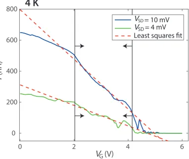
To determine the mobility of a wire, the slope ofISD in the linear regime is extracted
[image:16.595.132.515.143.465.2]from measurements at different source-drain bias voltages using a least squares fit. Figure 2.4 shows the fitting of two curves. Details of this method can be found in the supplementary info of [18].
V
G
(V)
I
(nA)
0
200
400
600
800
0
2
4
6
V
SDV
SD= 4 mV
Least squares fit
= 10 mV
4 K
Fig. 2.4: Plot ofISDvsVG forVSD = 10 mV (blue) and VSD = 1 mV (green). The red dotted lines show the fit made by the script using the least squares method.
2.2 Quantum dots
Quantum dots are small regions defined in a semiconductor with typical dimensions of around 100 nm. By application of electric fields, these dots can be gradually depleted of electrons or holes, so that a small, controlled number N is present. Because of coulomb repulsion, each added electron or hole requires additional an additional energy cost, causing electrons on these dots to occupy quantized energy levels. Figure 2.5 shows how these dots are formed electrostatically using two barrier gates and a plunger gate. Figure 2.6 depicts a schematic of a quantum dot with tunnel coupled source and drain contacts and a capacitively coupled gate (plunger).
VB
E
FV
PlungerTB
TB
V
Barrier1V
Barrier2Fig. 2.5: Schematic depiction of the band diagram of a single quantum dot.EF denotes the Fermi level, VB the valence band, TB a tunnel barrier and QD where the quantum dot is formed. Two tunnel barriers form a quantum dot with quantized energy states. VoltagesVBarrier1,VBarrier2andVP lungercontrol the height of the tunnel barriers and the energy levels of the dot.
Quantum dots can be described by the constant interaction model, which combines a quantized energy spectrum and the Coulomb blockade effect. Firstly, it assumes a constant dot capacitanceC=CS+CD+CG, the total capacitance which consists of
the capacitances between the dot and the leads (CS andCD) and that between the
dot and the gate (CG). Additionally, it is assumed that the single-particle energy-level
spectrum is independent of the number of electrons on the dot. These assumptions lead to a ground state energy of [19][21]
U(N) = [−|e|(N −N0+CgVg] 2
2C +
N
X
n=1
En(B) (2.7)
where N is the amount of electrons in the dot,VG is the applied gate voltage, B is
the applied magnetic field,N0is the charge in the dot compensating for background
V
SD+
-+
-V
gS
D
C
LC
RR
LR
RN
1C
GI
SDFig. 2.6: Schematic picture of a single quantum dot, its terminals and the corresponding capacitances and tunnel barriers.
The electrochemical potential of the dot is defined as the energy need to add another electron to the dot, and is derived as [19]
µdot(N) =U(N)−U(N−1) = (N −N0 1 2)EC−
EC
|e|CgVg+EN (2.8)
with the charging energyEC = e
2
C. Transitions between successive ground states are
spaced by the addition energy [21]
Eadd(N) =µ(N+ 1)−µ(N) =U(N+ 1)−2U(N) +U(N−1) =EC+ ∆E (2.9)
The addition energy can be zero when multiple electrons are added to the same spin-degenerate level.
To be able to observe this quantized charge tunnelling, two assumptions have to be made:
• (1) e2/C >> kBT The charging energy must be greater than the thermal
energy, which can be obtained by cooling the sample or decreasing dot size.
• (2) Rt >> h/e2 The tunnel barriers to the dot must be opaque enough to
localize the electrons i.e. the quantum fluctuations inN due to tunnelling off and on the dot is much smaller than one during the measurement timescale. This follows from the Heisenberg uncertainty principle∆E∆t= (e2/C)R
tC >
h. This implies that Rt should be much larger than h/e2 = 25.8kΩ, the
resistance quantum, which can be obtained by weakly coupling the dot to source and drain contacts.
Fig. 2.7: Diagram of the potential landscape of a quantum dot. µS, µD andµ(N)are the chemical potentials of the source, drain and dot.a)A dot in Coulomb blockade, no levels in the dot fall within the bias window, no transport is possible.b)A dot with a chemical potential level falling in the bias window, resulting in a tunnelling current. The amount of electrons in the dot changes betweenN andN−1. c)
[image:19.595.92.424.58.381.2]Current through the dot as a function of gate voltage, resulting in the characteristic Coulomb oscillations. The potential landscape around the dot changes between situationa)andb)as a function of the gate voltageVG. The peak spacing in this plot indicates the addition energyEaddtimesα, the lever arm of the gate [21].
Figure 2.7 shows the potential levels of the dot. If a level in the dot falls within the source-drain window, the number of electrons on the dot can alternate betweenN
andN+ 1and a tunnelling current is observed. If no levels fall in the window, the number of electrons on the dot is fixed and no tunnelling occurs: coulomb blockade. By adjusting the chemical potential of the dot usingVG, its different energy levels
can be aligned to the potential of the leads, lifting the coulomb blockade. Figure 2.7c shows a plot of the current versus the gate voltage, resulting in coulomb oscillations. Peaks indicate a fluctuation of the amount of electrons on the dot betweenN and
b)
a)
Fig. 2.8: Schematic diagrams of the potentials of a quantum dot in high bias regime. Gray levels indicate an excited state.a)VSDexceeds∆E, electrons can tunnel via two levels.b)VSDexceeds the addition energy, leading to double-electron tunnelling. [21]
.
WhenVSD is increased such that also a transition involving an excited state falls
within the bias window, two tunnelling paths are available for the electrons (Fig. 2.8a). Because the presence of an additional electron increases the charging energy, it is not possible for electrons to tunnel through these barriers simultaneously. This does lead to an increase in effective tunnelling rate. If the bias window is increased to be larger than the addition energy, double-electron tunnelling can take place. (Fig. 2.8b) [21]
2.2.1 Coulomb diamonds
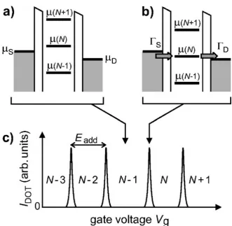
Plotting the conductance versusVSD and VG (bias spectroscopy) results in a plot
showing coulomb diamonds. At zero source-drain bias, conduction is only possible on specific gate voltages where a dot level exactly aligns withµ0. An increasing bias
voltage expands these points of conductance into ranges of gate voltage. At high bias multiple levels in the quantum dot conduct, resulting in double electron tunnelling. Inside the diamonds no conduction is possible and each diamond corresponds to a certain number of electrons on the dot, in the example shown for a depletion dot, an increasing gate voltage reduces the amount of electrons on the dot. To find out the exact amount, the last electron needs to be determined, which can be found by its non-closing corresponding diamond.
To form these diamonds, the drain is grounded and a voltage is applied to the source to obtain chemical potentials of µS = µ0 +eVSD and µD = µ0 where µ0 is the
potential for zero applied bias. The charge on the dot is constant i.e. no conduction is possible whenµdot(N) < µ0 andµdot(N + 1)> [µ0+eVSD]or in words, when
the energy levels in the dot lay outside the source-drain window (the situation in figure 2.7a). Combining this with equation 2.8 gives the following equations for the diamond edges forVSD >0:
0 = (N −1
2)EC−e(CG/C)VG+EN −µ0 (2.10)
eVSD= (N−N0+ 1
2)EC−e(CG/C)VG+EN+1−µ0 (2.11)
Finding aVSDthat satisfies both these equations (the crossing of the edges thus the
peak of the diamond) results ineVSD=EC+ ∆E and a difference in peak height
between subsequent diamondsN andN + 1 ofδE, assumingN + 1 corresponds to a new orbital level. ForVSD<0a similar exercise can be done to yield the other half
of the diamonds. The conversion factor between gate voltage and energyα =CG/C
follows from equation 2.8) and can be extracted from the diamonds as the ratio between its height and width. The slopes of CG/(C−CS) for tunnelling to the
source and−CG/CSfor tunnelling to the drain can be derived from the work needed
0
V
SDC/(C-C )
G S
-C /C
G
S
N+1 N
V
g
E =E +add C ΔE E =Eadd C
ΔE
b)
a)
Fig. 2.9: a)Schematic depiction of coulomb diamonds with its energies and equations for its slopes. No conduction is possible inside the diamonds.b)Example of coulomb diamonds (dI/dVSDvsVSDandVg5). [16]
2.3 Double quantum dots
While a single quantum dot is defined electrostatically by two barriers and a plunger gate (Fig.2.5), a double dot structure has two capacitively coupled plungers, two tunnel barriers to the source and drain from dot one and two respectively, and one tunnel barrier in between the dots (see figure 2.10).
The constant interaction model can be expanded from single quantum dots to
VSD
+
-+
-Vg1S
D
CL CM CR
RL RM RR
N
1N
2+
-Vg2
Cg1 Cg2
I
SDFig. 2.10: Schematic representation of a double dot system with its leads, tunnel barriers and capacitances. [20]
double quantum dots [20]. The double dot energy is now given by:
U(N1, N2) = 1 2N
2 1EC1+
1 2N
2
2EC2+N1N2ECm+f(Vg1, Vg2), (2.12)
with
f(Vg1, Vg2) = 1
−|e|[Cg1Vg1(N1EC1+N2ECm) +Cg2Vg2(N1ECm+N2EC2)] (2.13)
+1 e2[
1 2C
2
g1Vg21EC1+ 1 2C
2
g2Vg22EC2+Cg1Cg2Cg2Vg2ECm], (2.14)
whereN1(2),EC1(2),Cg1(2)andVg1(2)are the occupations number, charging energy,
gate capacitance and gate voltage for the first (second) dot, respectively. ECmis the
electrostatic coupling energy, the energy of one dot when an electron is added to the other. The different and capacitances energies can be related as:
EC1 = e2 C1
1
1− C2m
C1C2
EC2 = e2 C2
1
1− Cm2
C1C2
ECm=
e2 Cm
1
1−C1C2
C2
m
, (2.15)
SettingCm = 0 (the coupling between the dots), results in the mutual charging
energy ECm = 0, which reduces equation 2.12 to the sum of the energy of two
independent single dots. SettingCm ≈C1(2)results in a single large quantum dot
with a charge occupancy ofN1+N2.
More interesting is the region with intermediate coupling, resulting in a series double quantum dot.
Similar to the single quantum dot, the electrochemical potentialµ1(2)(N1, N2)of dot
1(2) is defined as the energy needed to add theN1(2)th electron to dot 1(2), while havingN2(1)electrons on dot 2(1). Its expression (in a way similar to equation 2.8)
is derived from equation 2.12:
µ1(N1, N2)≡U(N1, N2)−U(N1−1, N2) (2.16)
= (N1− 1
2)EC1+N2ECm− 1
|e|(Cg1Vg1EC1+Cg2Vg2ECm), (2.17)
µ2(N1, N2)≡U(N1, N2)−U(N1, N2−1) (2.18)
= (N2− 1
2)EC2+N1ECm− 1
|e|(Cg2Vg2EC2+Cg1Vg1EC2), (2.19)
2.3.1 Stability
From the chemical potential equations, a charge stability diagram can be constructed (Fig. 2.11), with equilibrium electron numbers N1(2) as a function of Vg1(2). By
changing the barrier potential between the dots, a system with weak, intermediate or strong interdot coupling can be formed. In weakly coupled or decoupled dots (Fig. 2.11a), the gate potential applied on one dot does not change the electron occupation of the other dot. When the coupling is increased, a hexagonal "honeycomb" structure (2.11b) appears, with so called "triple points" (dotted square). Increasing the coupling causes the dots to behave as one large dot with the combined charge of two dots (2.11c).
The triple points (Fig. 2.12a on page 19) form for double dots coupled in series (intermediately coupled dots). The tunnel barriers need to be sufficiently opaque to localize the electrons to a dot but still allow measurable transport. Conductance is only possible when electrons can tunnel through both dots (this requires three available states), so both dot potential levels align with the source and drain (as seen in figure 2.13a).
Two points are distinguished, state corresponding to two different charge transfer processes. One around the (0,0) state indicated by•and pathein Fig. 2.12a.
(N1, N2)→(N1+ 1, N2)→(N1, N2+ 1)→(N1, N2)
and one around the (1,1) state, indicated byand pathh:
(N1+1, N2+1)→(N1+ 1, N2)→(N1, N2+ 1)→(N1+ 1, N2+ 1)
The energy difference between these cycles determines the spacing between these points, and is given byECm. The other dimensions of the honeycomb cells (figure
2.12b) can be related to the capacitances from equation 2.15 [20].
∆Vg1 =
|e|
Cg1
(2.20)
∆Vg2 =
|e|
Cg2
(2.21)
∆Vgm1 = |e|Cm Cg1C2
= ∆Vg1 Cm
C2
(2.22)
∆Vgm2 = |e|Cm Cg2C1
= ∆Vg2 Cm
C1
(2.23)
b)
a)
Fig. 2.12: a)Zoom of a triple point, indicating the two possible ways of transport: hole transfer and electron transfer. b)Schematic of one honeycomb cell from the stability diagram, indicating the spacings between coulomb peaks. [20]
2.3.2 Bias triangles
A bias voltage to the source and grounding the drain (µL = −|e|V and µR = 0)
couples to the double dot through the source capacitanceCL. This causes these
triple points to expand into triangular regions, bounded by the conditions: −|e|V = µL > µ1, µ1 > µ2, and µ2 > µR = 0. δVg1 and δVg2 are now related to the bias
voltage as:
α1δVg1 =
Cg1 C1|e|δVg1
=|eV| α2δVg2 =
Cg2 C1|e|δVg2
=|eV| (2.24)
whereα1andα2 are the conversion factors (lever arms) between gate voltage and
energy [20].
b)
a)
Fig. 2.13: a)Schematic representation of the triple points between charge states (region in dotted square of figure 2.11. Four charge states are present, separated by solid lines. At the solid line connecting the two triple points, the state (0,1) and (1,0) are degenerate.b)Effect of a finite bias. Current can flow in the triangular gray regions. [20]
2.3.3 Pauli spin blockade
Electrons can have either a spin up or a spin down. When no magnetic field is present, these states are degenerate i.e. have the same energy. Applying a magnetic field splits the two spin states in energy by the Zeeman energy[21]. Using this energy difference, Pauli spin blockade can be formed i.e. spin dependent tunnelling. It can be utilized to implement spin-to-charge conversion in double quantum dot. This has been experimentally realised in different double quantum dot systems [34][35][36][17].
Figure 2.14 illustrates this effect.[21] A spin blockade occurs in one bias direction due to the energy difference between two spin states. With (N1, N2) = (0,1), at
negative bias, the transfer sequence: (0,1)→(0,2)→(1,1)→(0,1)occurs. There is permanently one electron on the right dot, which excludes another electron with the same spin from entering the dot due the Pauli exclusion. Only an opposite spin can be added, forming the singlet state S(0,2). From this state, one electron can tunnel to the left lead via the left dot.
In contrast, at positive bias the transfer sequence: (0,1)→(1,1)→(0,2)→ (0,1)
occurs, and electrons with either spin state can tunnel onto the left dot, independent of that of the left dot. If these form the singlet stateS(1,1), the electron can tunnel to the right lead via the right dot. Otherwise, a triplet stateT(1,1)is formed and no transport is possible due toT(0,2)being too high in energy. Relaxation of the spin state allows the electron to tunnel, but due to the relaxation time, this current is negligible. A bias voltage exceeding the singlet-triplet splitting EST enables
tunnelling from theT(1,1)to theT(0,2), lifting the spin blockade.
b)
a)
Fig. 2.14: Schematic and measurements of Pauli spin blockade.a)Potential diagrams of the different regimes in bias triangles illustrating the process of Pauli spin blockade. In the one electron regime (top row), transport is possible at positive and negative bias. In the two-electron regime (bottom row) however, this is not possible for a negative bias. Color edges ofa)represent points in the experimental results
b)Double dot current as a function ofVLandVR. Insets: simple rate equation predictions of charge transport. Image from [21], reproduced from [37].
Fig. 2.15: Schematic of a spin initialization, manipulation and read process, controlled by a combination of a voltage pulse and burst.[38]
3
Fabrication and measurement
setup
This chapter explains the device design and the fabrication steps involved to create successful devices. The two main types of devices are shown: a field effect transistor (FET) device (Fig. 3.1a), which is used for characterisation of nanowires, and bottom gated nanowire devices (Fig. 3.1b), used for measuring quantum dots. Both devices consist of with a p++ doped <100> Si substrate with a 105 nm layer ofSiO2on
top. Wires are deposited either directly on the sample or on bottom gate structures. The bottom gate structures consist of Ti/Pd gates with a very small pitch, covered inAl2O3. As last step, Ti/Pd source and drain contacts are deposited on the wires.
The designs of the devices are explained, as well as different generations of bottom gate devices. The process flow can be found in appendix A. The chapter ends with showing a finished sample and the setup used to conduct measurements on the nanowire.
Si
SiO2
Al2O3
g1 g2 g3 g4 g5 g6
15nm 15nm
105nm 50nm
nanowire
nanowire
S D
Ti/Pd
S D
a)
b)
550nm
40nm
700nm
Fig. 3.1: Schematic cross-sections ofa)A FET device with 700 nm spaced 0.4/50 nm thick Ti/Pd source (S) and drain (D) contacts on a nanowire directly on the sample (a p++ doped Si substrate with a 105 nm layer ofSiO2).b)A device with a nanowire on 40 nm pitch, 0.4/15 nm thick Ti/Pd bottom gates (g1-g6), encapsulated in 15 nmAl2O3. Dimensions vary between different generations of devices.
10 µm
2 µm
5 µm
b)
c) d)
20 µm
a)
Fig. 3.2: Deposition of nanowires using a Micro Manipulator. Optical microscope images of
a)Part of the nanowire growth chip. b)A wire on the tip.c)A wire deposited on bottomgates. A low light intensity is used to attempt to increase the visibility of the wire.d)AFM image of the same wire, confirming it’s deposition.
3.1 Wire deposition
In order to make bottom gated devices, nanowires need to be deterministically place on top of bottom gates with high precision. In order to do this, we use a Micro Manipulator (Kleindiek MM3A-EM). This tool consists of a sharp tip (≈100 nm diameter) on an arm which can be displaced in the X, Y and Z direction and rotated around its axis using piezo elements. Wires are picked up from or broken off the growth chip (Fig. 3.2a and b), and then put down either directly on the chip for nanowire FET devices or on a set of bottom gates (Fig. 3.2c). Vanderwaals forces cause the nanowire to stick to the substrate when laid down.
1 mm
20 µm
20 µm
20 µm
b)
c)
a)
d)
S D
1 µm
Fig. 3.3: Design of a nanowire FET device.a)Overview of the chip.b)A single writefield, the unit cell of the design.c)A deposited nanowire. Inset: AFM image of the wire.
d)Source and drain contact design for the nanowire.
3.2 FET devices
To characterize the performance of the nanowires, devices similar to field effect transistors (FETs) are fabricated. Source and drain contacts are patterned onto the deposited nanowires, explained in Fig. 3.3, while the substrate will serve as a global back-gate. The first layer is fabricated using optical lithography, contact pads of 200 by 200µm are patterned and connected to smaller structures. The big pads are connected to the paths seen on the edges of Fig. 3.3a. Markers are patterned on each field of 100 by 100µm(Fig. 3.3b) using electron beam lithography (EBL) on a layer of PMMA.
Titanium and palladium (Ti/Pd) structures are deposited using electron-beam evap-oration and lift off. These markers encode for a specific location on the sample and are used to locate deposited nanowires by aligning microscope images to the design (Fig. 3.3c). Cross shaped markers are also written to align an EBL pattern with the source drain contacts to the nanowires, seen in Fig. 3.3d. Before depositing metal, the silicon oxide covering the wire needs to be etched, to ensure good contact. This oxide has grown while the wire was exposed to ambient conditions: during deposition. Etching is done using 12,5% buffered hydrogen fluoride, and imme-diately after a metal layer of 0.5 nm titanium and 50 nm palladium is deposited using e-beam evaporation and lift-off. Titanium is used as a sticking layer for the palladium, while palladium is chosen because its work function matches the electron affinity of germanium [39], thus allows for good ohmic contacting. An AFM image of a fabricated device can be seen in Fig. 3.5b.
3.3 Bottom gate devices
To form tunable hole quantum dots, we fabricate devices with nanowires on bottom gates. These structures consist of 6 gates (0.4nm/15nm Ti/Pd) covered in 15 nm
Al2O3 (Fig. 3.4b) and are patterned in the middle of the fields using EBL as seen in
Fig. 3.4a. After deposition, promising wires are contacted using an additional EBL step aligned to markers written simultaneously with the gates. An AFM image of a finished device can be seen in Fig. 3.5a.
Various processes and parameters in the bottomgate design can be tuned or changed. This section will cover a few important aspects which were improved.
3.3.1 Pitch
The pitch of the bottom-gates is critical for reaching the single-hole regime without splitting the dot into a double dot, which became evident in the previous generations of devices with a pitch of 100 nm [15].
40nm 550nm
b)
c)
100nm 900nm
a)
g1 g2
g3 g4 g5
g6
Fig. 3.4: Design of a bottom-gated nanowire device. Colors represent the dose used for each structure.a)Overview of a writefield. b)The bottom gate structure, consisting of the gates (orange and green), an oxide layer (blue) and pads to supply a flat surface for the nanowire to attach to (red). The oxide layer actually covers the whole structure. c)A zoom of the gate structure.
1 µm 1 µm
b) a)
S
D
S
D
g1 g2 g3
g4 g5 g6
Al2O3
Fig. 3.5: AFM images ofa)A bottomgate device (with an older design of oxide windows) andb)A typical nanowire FET device.
b)
c)
a)
d)
2 µm
g1
g2
g3 g4 g5
g6
2 µm
g1
g2 g3 g4
g5 g6 Al2O3
Fig. 3.6: AFM images ofa)40 nm pitch gates andb)60 nm pitch embedded gates with height profiles taken at the red lines forc)40 nm pitch gates. d) 60 nm pitch embedded gates. Blue lines mark the centres of the outermost gates, which are separated by five times the pitch.
Now, exposure by scattering electrons [42] is the limiting factor of the feature size. A decrease in thickness of the PMMA layer reduces the path length for an electron to scatter, thus also the width. A reduction from 85 to 55 nm allowed for pitches down to 40 nm (Fig. 3.6a and c).
3.3.2 Embedded gates
The smoothness of the bottom gate structures has an effect on the nanowire deposi-tion: wires stick better to smooth surfaces due to a higher contact area.
To obtain a more even surface, the gates can be embedded in the silicon oxide layer (Fig. 3.6b and d). Before depositing metal on the developed gate patterns, a 12,5% BHF etch is used to etch a trench in theSiO2 approximately as deep as the thickness
of the gates. The etch is isotropic, causing it to also etch theSiO2 in between the
trenches. Etching away theSiO2 below the PMMA bridges separating the trenches
3.3.3 Gate oxide
Previously, theAl2O3 covering the sample was etched using 12,5% BHF. Problems
arise from the aggressiveness of this etchant: it has a fast etch rate ( 1 nm per second) etches theSiO2 layer too. When attempting to etch layers thicker than 15
nm, the resist covering the gates would be removed during the etch causing the oxide to be attacked, and slight over etches resulted in attack of the silicon oxide layer.
To be able to etch thicker layers ofAL2O3, another etchant is used:
Tetramethy-lammonium hydroxide. TMAH is selective toAL2O3and etches at a rate of∼1 nm
per 40 seconds. Coincidentally, this is the main ingredient of the developer used for the etching mask, allowing us to develop and etch in one step. The timing of this process is non critical and results in a 100% yield of the gate oxide layer.
3.3.4 Oxide capping
To increase the coupling between the gates and the wire, devices are capped with an additional layer ofAl2O3 all over the sample, grown by atomic layer deposition at a
temperature of 100 °C. Higher temperatures have been found to destroy nanowires. This layer embeds the wire inAl2O3, increases the coupling between the gates and
the nanowire by a factor 1.8 [43].
3.4 Measurement preparations and setup
Finished chips are "glued" to a printed circuit board using PMMA/copolymer. Wires connect the contact pads on the chip and those on the PCB (Fig. 3.7). These are made using a W7476E Wedge-wedge wirebonder, which uses ultrasonic energy to "weld" aluminum wires to a substrate. The contacts on these PCB’s can be connected to the wiring in a dipstick or dilution refrigerator and then be addressed using a Delft Electronic IV/VI rack. The PCB’s are mounted in a dipstick and lowered into a dewar of liquid helium (4.2K). A metal canister shields the sample from electromagnetic interference and a temperature sensor is in place to be able to confirm that the sample is at liquid helium temperature.
After loading a sample, the contacts on the PCB are connected to the IV-VI rack. This setup contains low noise voltage sources and current measurement units. To reduce noise from the power grid, it is connected optically to the controlling computer and is powered by batteries.
4
Results and discussion
In this chapter, the results of the measurements performed on successful devices are presented. First, we show the determined mobilties for multiple low diameter nanowire FET devices. Secondly, we were able to create single and double quantum dots in one of the bottom gate devices and show measurements of coulomb diamonds and bias trangles. Lastly, to better understand the effects of UV ozone treatment andAl2O3 capping, measurements of bottom gate devices are shown for different
treatments of the device.
4.1 Mobilities
At the start of this thesis, I have fabricated several nanowire FET samples with low diameter wires, because more low diameter data points were needed for a paper about mobility in Si-Ge core-shell nanowires [18]. The resulting mobilities can be found in Fig.4.1. This data confirms that low diameter wires have a higher mobility, with a maximum measured mobility of (4267 ± 219) cm2V−1s−1 in a 15 nm diameter nanowire. This is much higher than the previously reported values [26][44]. TEM studies have shown that the highest mobility wires all had a <110>crystal orientation, confirming that these wires have the lowest defect density.
When forming quantum dots, it is essential to have a low defect density so no unintentional dots are formed. Contrary to the previous studies [24] the mobility is found to decrease dramatically due to an increased temperature. It is possible that the effect of phonons only becomes relevant at a low defect density.
10 20 30 40 50 0
1000 2000 3000 4000 5000
(c
m
2 /V
s)
Wire diameter (nm)
µ
4 K 295 K
Fig. 4.1: Graph of the extracted mobilities versus wire mobility. A significant increase is observed for low diameter wires. Image courtesy of Joost Ridderbos.
S
D
S
D
S
D
b)
a)
BarrierPlunger Interdot
Fig. 4.3: Configurations of gates used to form single dotsa)left dot andb)right dot.
4.2 Single quantum dot
This section explains the formation of a quantum dot in a nanowire using the finegates and shows the resulting coulomb diamonds and stability diagrams. Unless stated otherwise, all measurements are done with a source drain voltage (VSD) of
1mV.
To characterize the effect of the gates on the conductance of the wire, we measure source-drain current as a function of gate voltage for each gate, as seen in figure 4.2. Increasing a gate voltage locally decreases the amount of charge carriers in the wire, with a decreasing conductance as result, until current is blocked (pinch-off). Different gates have a different effect, mainly due to inhomogeneities in the wire and partly due to an inhomogeneous oxide layer. Gate 6 in particular shows multiple resonances around its pinch-off voltage, indicating the presence of an unintentional dot due to a defect. Pinch-off using gate 1 is not possible (the voltage source is limited to 12 V), this could be due to the close presence of the source contact (see appendix C), influencing the electric field. Ideally, you want to see pinch-off without resonances, indicating that no unintentional quantum dots are formed.
To form and tune a singular quantum dot, three gates will be used. Two to tune tunnel barriers to source and train respectively (barrier gates) and one to influence the dots energy levels (plunger gate) (Fig. 4.3). Two different configurations are used.
4.2.1 Stability maps
First, stability maps are made using the barriers (Fig. 4.4a and 4.5a). Additional resonances not coupled equally to both gates (green arrows Fig. 4.4b and 4.5b) indicate that you are not (exclusively) forming an intentional quantum dot between the two barriers, but that unintentional dots are also formed due to defects. These are usually very small, so have slower resonances as a function of gate voltage. For these quantum dots, there is cross coupling between adjacent gates i.e. the barriers partly act as plunger and vice versa. To make sure the dots tunnel barriers are not too high when also applying a plunger gate voltage, additional maps are made while having a fixed voltage on the plunger (Fig.4.4b and 4.5b). We observe that the gate voltages required to pinch-off are lower.
In both stability maps, regular diagonal resonances can be observed. Diagonal lines result from a quantum dot equally coupled to both gates, indicating it is a (likely intentional) dot formed in between the gates. Barrier voltages that result in such a regime are used as parameters for a bias spectroscopy.
12000 11600 11400 11200 11000 11800
8600 8800 9000 9200 9400 0.9 0.3 -0.3 -0.9 -1.5 log(I SD )(n A ) -0.6
Vg2(mV) Vg4 (m V ) 12000 11500 11000 10500 10000
6000 6500 7000 7500 8000 1.2 0.4 0.0 -0.8 -1.6 log(I SD )(n A ) -0.4
Vg2(mV) Vg4 (m V ) -1.2 0.8 -1.2 0.6 0.0
Vg3 = 5500 mV Vg3 = 0 mV
Fig. 4.4: Plots of log(ISDvsVg2andVg4for the left dota)without using the plunger andb) with the plunger at 5.5 V. Resonances in the direction of gate 4 are marked with a green arrow. The blue circle indicates the point chosen for bias spectroscopy measurements (Fig. 4.6a).
12000 11600 11400 11200 11000 11800
6000 6500 7000 7500 9000
1.2 0.4 -0.4 -1.2 log(I SD )(n A ) -0.8
Vg6(mV)
Vg4 (m V ) -1.6 0.8 0.0 8500 8000 12000 11600 11400 11200 11000 11800
6000 6500 7000 7500 9000
0.6 0.0 -0.6 -1.2 log(I SD )(n A ) -0.9
Vg6(mV)
Vg4 (m V ) -1.5 0.3 -0.3 8500 8000 0.9 a)
b) Vg5 = 5000 mV
Vg5 = 0 mV
Fig. 4.5: Plots of log(ISD vsVg2 andVg4 for the right dota)without using the plunger andb)with the plunger at 5 V. Resonances in the direction of gate 6 are marked with a green arrow. The blue circle marks the point chosen for bias spectroscopy measurements (Fig. 4.6b).
4.2.2 Coulomb diamonds
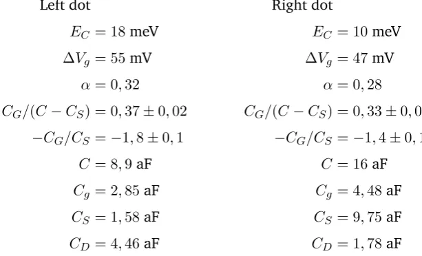
Figure 4.6 shows bias spectroscopies (conductance as a function of gate and source-drain voltage) measured on both quantum dots. Charging energies, coulomb peak spacings and slopes can be extracted from the diamonds, allowing us to calculate the corresponding capacitances, as explained in section 2.2.1. These properties are constant over the regime shown in Fig. 4.6. Left (right) dot denotes the dot formed between gates 2 and 4 (4 and 6) (Fig.4.3).
Left dot Right dot
EC = 18meV EC = 10meV
∆Vg = 55mV ∆Vg = 47mV
α= 0,32 α= 0,28
CG/(C−CS) = 0,37±0,02 CG/(C−CS) = 0,33±0,02
−CG/CS =−1,8±0,1 −CG/CS=−1,4±0,1
C = 8,9aF C= 16aF
Cg = 2,85aF Cg = 4,48aF
CS = 1,58aF CS= 9,75aF
CD = 4,46aF CD = 1,78aF
The difference in charging energy indicates differently sized dots. In principle, both dots should have the same size in a defect free wire. Assuming the length of the gate defined dots to be the distance between the inner edges of the barrier gates, using a tunnel barrier width of∼30 nm, the resulting dot length is 90 nm for both dots. Comparing these charging energies to those of dots in previous generation devices [15], the left dot has a charging energy of 18 meV, similar to a dot of 60 nm length (18,3 meV). The right dot has a charging energy of 10 meV, similar to a dot of 160 nm length (10,2). The different charging energy between the dots shown here is attributed to an additional unintentional dot beneath gate 6. This dot is highly coupled to the intentional dot, resulting effectively in a larger dot.
The difference in gate capacitance is also attributed to this larger dot size.
-1.2 -2.4 -3.6 -4.8 -4.2 -5.4 -1.8 -3.0 -0.6 log(|dI SD /dV SD |)(e 2/h)
Vg5(mV)
10 0 -5 -10 5 VSD (mV ) -1.5 -2.5 -3.5 -4.5 -4.0 -5.0 -2.0 -3.0 -1.0
4000 4250 4500 Vg4 = 11800 mV, Vg6 = 7050 mV
b) Vg3(mV)
5600 5800 6000
20 0 -10 -20 10 VSD (mV )
Vg2 = 7450mV, Vg4 = 11800mV
a) log(|dI SD /dV SD |)(e 2/h)
Fig. 4.6: Bias spectroscopies (log()|dISD/dVSD|) vsVgof quantum dots formed ina)The left dot (Fig. 4.4b) andb)the right dot (Fig. 4.5b) at the blue circles.
4.3 Double quantum dot
Double quantum dot systems can be formed using five gates, as shown in Fig. 4.7. Two gates are used to tune the coupling of the left and right dot to source and drain respectively, one is used to tune the interdot coupling and are two gates as plungers for both dots respectively.
S
D
S
D
S
D
Left dot
Right dot
b)
a)
Barrier
Plunger
Interdot
Fig. 4.7: Configuration of gates used to form a double dot.
4.3.1 Stability maps
First, similar to single quantum dots, a stability map is made using the outer barriers (Fig. 4.8a) to determine a regime where a stable intentional dou-ble quantum dot can be formed. This measurement is done with the plungers and interdot gates at a fixed voltage which causes a singular quantum dot to split up, thus forming a double dot system between the barriers. We can observe that the lines are not diagonal:
the left dot has a higher coupling to the left barrier than the right dot to the right barrier. This is due to the lower charging energy (thus larger size) of the right dot (Fig. 4.6). In Fig. 4.8b the diagram starts to resemble the honeycomb structure characteristic for intermediately coupled double dots, as explained in section 2.3 [20]. Lines in the vertical direction show a decrease and increase in current due to an additional unintentional dot formed beneath gate 6 (also observed in Fig 4.2 and 4.5. Further decreasing the interdot coupling and increasing the outer barriers results in bias triangles appearing (Fig. 4.8b). This is caused by the barriers partly functioning as plunger due to cross coupling.
7400
6800
6400
6000 7200
6600 7000 7400 7800 8000
0.3 -0.3 -0.9 -1.5 -2.1 log(I SD )(nA ) -1.2
Vg2(mV)
Vg4 (mV ) -1.8 0.0 -0.6 Vg3 = 5000 mV,
Vg4 = 9500 mV
Vg5 = 5000 mV
6600
6300
6200
6100 6500
7300 7400 7600 7800
-0.3 -0.9 -1.5 -2.1 log(I SD )(nA ) -1.2
Vg2(mV)
Vg4 (mV ) -1.8 0.0 -0.6 6400 7700 7600 6500 6300 6200 6100 6400
6900 7000 7200 7300
-0.4 -1.2 -2.0 -2.8 -3.6 log(I SD )(nA ) -2.4
Vg2(mV)
Vg4 (mV ) -3.2 -0.8 -1.6 7100 7400 6600
Vg3 = 6000 mV,
Vg4 = 9500 mV
Vg5 = 6000 mV
Vg3 = 5000 mV,
Vg4 = 9500 mV
Vg5 = 5000 mV
a)
b) c)
Fig. 4.8: Plots off log(ISDvsVg2andVg6for the double dot configurationa)Large map.b) More precise measurement of a small area.c)The same area with tuned interdot coupling and tunnel barriers.
Diagonal lines (marked by blue arrows) reveal an additional resonance (along the green arrow) compared to a double dot stability map (Fig. 2.11b), which is equally affected by both plunger gates. We interpret these as quantized charge states of a third (unintentional) quantum dot located beneath gate 4. Changing the energy levels in this middle dot has a similar effect to changing the interdot coupling. A honeycomb pattern can be observed at the region marked by a blue square, indicating an intermediately coupled double quantum dot. Parallel lines can be observed in the region marked by a green square, indicating a strongly coupled quantum dot, starting to resemble a single quantum dot. Lastly,the tunnel current due to the left and right barrier goes down with an increasingVg3andVg5respectively,
due to cross coupling to their neighbouring barrier gates. Cross coupling to the plunger also reduces the the tunnel current as well as the coupling between the dots.
6550
6400
6350
6300 6500
6100 6150 6250 6350
-1.00 -1.50 2.00 -2.50 log(I SD )(nA ) -1.75
Vg3(mV)
Vg5 (mV ) -2.25 -0.75 -1.25 6450 6300 6200 6700 6500 6400 6300
6100 6200 6400 6500
-1.2 -1.6 -2.0 -2.4 log(I SD )(nA ) -1.8
Vg3(mV)
Vg5 (mV ) -2.2 -1.0 -1.4 6600 6300 6600 5800 5400 6200
5400 5800 6200 6600
-0.4 -1.2 -2.0 -2.8 log(I SD )(nA ) -2.4
Vg3(mV)
Vg5 (mV ) -3.2 -0.8 -1.6
Vg2 = 7250 mV Vg4 = 9500 mV Vg6 = 6300 mV
Vg2 = 7250 mV Vg4 = 9500 mV Vg6 = 6300 mV Vg2 = 7150 mV Vg4 = 9500 mV Vg6 = 6300 mV
a) b) c) ΔVg5 ΔVg3 ΔVg3,M ΔVg5,M
Fig. 4.9: Plots off log(ISD vsVg3 andVg5 for the double dot configuration, showing the effect of the plunge gates. a)Large map with lots of features b) Zoom of a)
4.3.2 Bias triangles
We now look for an area with clear bias triangles. Due to cotunneling, transport can still take place outside the bias triangle pairs via intermediate states. Suppressed cotunneling indicated by a low tunnel current along the honeycomb edges. A region from Fig. 4.9 (marked by a white rectangle) that shows this behaviour is zoomed in upon (Fig. 4.9b,c). From fig. 4.9c, we determine the voltages needed to add a hole to the left (right) dot∆Vg3 (∆Vg5) and calculate the corresponding capacitances
using equation 2.23[20].
We observe that there is a mutual capacitive couplingCM that leads to a separation
between the two triple points [20]. This shift is equal to the separation between the bias triangles (and incidentally equal to the size of the bias triangles) and can be expressed in terms of the voltages∆Vg3,M and∆Vg5,M (Fig. 4.9c). Corresponding
mutual capacitances can be calculated using equation 2.23 [20].
Lever armsα3andα5for both gatesδVg3andδVg5are now calculated using equation
2.24[20] with |eV| = 1 meV due to the 1 mV source-drain bias. The capacitances
CLef tdot,CRightdotandCM can now be calculated via 2.23[20]:
Left dot Right dot
EC,Lef tdot= 5,2meV EC,Rightdot = 4,6meV
∆Vg3 = 60±2mV ∆Vg5 = 53±2mV
Cg3 = 2,67aF Cg5 = 3,02aF
αg3 = 0,083 αg5 = 0,083
δVg3 = ∆Vg3,M = 12±1mV δVg5 = ∆Vg5,M = 12±1mV
Cg3,M = 0,53aF Cg5,M = 0,68aF
CLef tdot = 32aF CRightdot= 36aF
CM = 7,74aF EM = 1,04meV
The gate capacitances are all about a factor two lower than those in previous devices [15] which can be explained by having a thicker gate oxide (25 vs 10 nm). Mutual capacitances are approximately equal. We assume that the increase in capacitance due to oxide thickness is compensated for by a decrease in pitch. Individual dot charging energies are about half, as is the mutual charging energy. This has also been seen in the single dot measurements, and is attributed to increase in length of the quantum dots due to defects in the wire.
Note that these measurements were performed at 4.2 Kelvin as opposed to in a dilution refrigerator with a base temperature of 8 mK for the previous devices [15], so the resolution of these measurements is limited.
12000
10000
9000 11000
9000 10000 11500
0.5
-0.5
-1.5
log(I
SD
)(nA
)
-2.0
Vg3(mV)
Vg4
(mV
)
0.0
-1.0
10500
-2.5
9500 11000
Fig. 4.10: Plot of log(ISD) vsVg1andVg2. This shows that no quantum dots are formed between adjacent gates.
4.4 Quantum dots between adjacent gates
As a final quantum dot experiment, we attempt to form a quantum dot between two adjacent gates. As seen in Fig. 4.10, no regular resonances coupled equally to both gates can be observed, indicating no intentional quantum dot is formed. This provides sufficient evidence that double quantum dots will not split up into two dots with the plunger gate acting as barrier.
Fig. 4.12: ISD vs Vg curves for two different gates before (circles) and after (squares) capping withAl2O3and after subsequent UV Ozone treatment (stars).
4.5 Effect of UV Ozone
[image:50.595.148.491.69.257.2]A big difference between this generation of devices and the older generation with 100 nm pitch gates is the higher electric field required to pinch off (Fig. 4.2). This is attributed to the increase in oxide thickness from 10 to 25 nm, reducing gate capacitance. The different gate design could also have an effect, but simulations are needed to investigate the gate behaviour. Another cause could be the effect of treating the sample in a UV ozone reactor. An increase in pinch off voltage could be the result of removing positive charge or adding negative charge inAl2O3.
Figure 4.11 shows the effect of a UV ozone treatment on the pinch of curves of another device. While previously we were able to pinch the current with both gates, this is no longer the case after treatment. The saturation current has also increased from 20 nA to 25 nA.
Figure 4.11 shows the effect of capping a wire with anAl2O3 layer and subsequent
UV ozone treatment. Both gates have a lower pinch off voltage after capping. This is expected because the gate coupling is increased due to the nanowire now being embedded in oxide [43]. This does not explain the decrease in saturation current from 28 to 20 however. Contrary to an uncapped sample, UV Ozone treatment now reduces the pinch off voltage and also changes the gate behaviour.
The decrease in pinch off voltage could be a result of adding positive charge or removing negative charge in theAl2O3. Similarly an increase could be the result of
removing positive charge or adding negative charge inAl2O3.
We can conclude based on these measurements that it seems UV ozone has the effect of shifting pinch off voltages towards lower values when the devices is capped withAl2O3. We do not currently understand the exact mechanism however. More
statistics are needed to determine the exact behaviour and the cause of this effect.
5
Conclusion
A successful change in the design and fabrication procedure was made, resulting in bottom gate structures with gates with a pitch of 40 nm and with embedded gates with a pitch of 60 nm. Oxide thicknesses of over 15 nm are also possible now.
Single and double quantum dots have been observed in one device with 60 nm embedded gates at 4.2 K. A decrease of single dot charging energies compared to a previous 100 nm pitch device is attributed to unintentional quantum dots due to defects in the wire, effectively increasing dot size.
The resonances seen in the stability map of the double dot are explained by an additional unintentional dot mediating the coupling between the two intentional dots. Bias triangles have been observed, but measurements at 4.2 K experienced too much thermal noise to extract accurate data.
We were not able to form a quantum dot between adjacent gates, which indicates that we should be able to reach the single regime without the dot splitting up with a clean enough device. We were not able to reach the single hole regime in the measured device.
Additionally, a decrease in lever arm of the gate has been observed. We attribute this to a decreased capacitance due to the thicker oxide and cross coupling between gates due to the lower pitch.
The cause of the increased pinch off voltage is still unclear. UV-Ozone has an effect that still needs to be investigated.
6
Outlook
In this thesis, 4.2K measurements of bias triangles in double quantum dots were shown. The single hole regime could not be reached due to a too high defect density in the wire. In this measurement setup, thermal noise is too large to observe excited states. The plan was to load device in the triton setup, so we can perform experiments with magnetic fields and high frequency electronics. This would allow us to set up Pauli spin blockade [17], read it out using single-shot readout [45] and try and manipulate spin states using RF electric fields [29]. We would then be able to experimentally investigate the theoretical predictions about Si-Ge core-shell nanowires [29].
Unfortunately, the measured device was sent to quantum heaven by a static shock (see appendix C).
This brings us to the bottleneck for these experiments: successfully fabricating low diameter nanowire bottom gate devices. It proves difficult and laborious to find and deposit thin nanowires, due to the limits of the optical microscope and the large amount of thicker wires present. During subsequent fabrication steps wires could still move or break. Improvements could be made to the design to be more flexible for the location of nanowires, for example increasing the length of the and amount of gates. Now, multiple wires can be deposited allover the gate array, and source and drain contacts are only patterned on one nanowire per gate structure. This also improves the chances of finding thinner wires, as these are very hard (sometimes impossible) to see and thus the thinnest wires are rarely deliberately picked up. Furthermore, more than 6 gates could be used to form a multi dot system in a single long nanowire, and transport a spin state across multiple quantum dots. Wires of a fewµm length are not uncommon, easily allowing for 15 gates to form 7 quantum dots.
As a final remark, UV-ozone treatments still have an unclear effect on the electrical properties of both wires and sample. Previously, this method has been used purely as a cleaning step, but more care should be taken in the future.
Bibliography
[1]Richard P. Feynman. „Simulating physics with computers“. In:International Journal of Theoretical Physics21.6-7 (1982), pp. 467–488. arXiv:9508027 [quant-ph](cit. on p. 3).
[2]J. Ignacio Cirac and Peter Zoller. „Goals and opportunities in quantum simulation“. In:
Nature Physics8.4 (2012), pp. 264–266 (cit. on p. 3).
[3]P. Shor. „Polynomial-Time Algorithms for Prime Factorization and Discrete Logarithms on a Quantum Computer“. In:SIAM Journal on Computing26.5 (1997), pp. 1484–1509. arXiv:9508027 [quant-ph](cit. on p. 3).
[4]L K Grover. „Quantum Mechanics Helps in Searching for a Needle in a Haystack“. In:
Physical Review Letters79 (1997), p. 325. arXiv:9706033 [quant-ph](cit. on p. 3). [5]B. P. Lanyon, J. D. Whitfield, G. G. Gillett, et al. „Towards quantum chemistry on a
quantum computer“. In:Nature Chemistry2.2 (2010), pp. 106–111. arXiv:0905.0887
(cit. on p. 3).
[6]A. Aspuru-Guzik. „Simulated Quantum Computation of Molecular Energies“. In:Science
309.5741 (2005), pp. 1704–1707 (cit. on p. 3).
[7]Daniel S. Abrams and Seth Lloyd. „Quantum Algorithm Providing Exponential Speed Increase for Finding Eigenvalues and Eigenvectors“. In:Physical Review Letters83.24 (1999), pp. 5162–5165. arXiv:9807070 [quant-ph](cit. on p. 3).
[8]Craig R. Clark, Tzvetan S. Metodi, Samuel D. Gasster, and Kenneth R. Brown. „Resource requirements for fault-tolerant quantum simulation: The ground state of the transverse Ising model“. In:Physical Review A79.6 (2009), p. 062314 (cit. on p. 3).
[9]Chenyang Wang, Jim Harrington, and John Preskill. „Confinement-Higgs transition in a disordered gauge theory and the accuracy threshold for quantum memory“. In:Annals of Physics303.1 (2003), pp. 31–58. arXiv:0207088 [quant-ph](cit. on p. 3).
[10]Austin G Fowler, Matteo Mariantoni, John M Martinis, and Andrew N Cleland. „Surface codes : Towards practical large-scale quantum computation“. In: (2012) (cit. on p. 3).
[11]M. Veldhorst, C. H. Yang, J. C. C. Hwang, et al. „A two-qubit logic gate in silicon“. In:
Nature(2015), pp. 0–4 (cit. on pp. 3, 5).
[12]Jarryd J. Pla, Kuan Y. Tan, Juan P. Dehollain, et al. „A single-atom electron spin qubit in silicon“. In:Nature489.7417 (2012), pp. 541–545. arXiv:1305.4481(cit. on p. 3).