Implementation of Binary Extension Field for
Quad Core Cryptoprocessor on FPGA
T.Priyadarsini
1, V.Thiyagarajan
2, M.Mohanraj
3, K.Saipriya
4Assistant Professor, Dept. of ECE, V.R.S. College Of Engineering And Technology, Arasur, Villupuram District,
Tamilnadu, India1
Associate Professor, Dept. of ECE, V.R.S. College Of Engineering And Technology, Arasur, Villupuram District,
Tamilnadu, India2
Final Year, UG Student, Dept. of ECE, V.R.S. College Of Engineering And Technology, Arasur, Villupuram District,
Tamilnadu, India3
Final Year, UG Student, Dept. of ECE, V.R.S. College Of Engineering And Technology, Arasur, Villupuram District,
Tamilnadu, India4
ABSTRACT: This paper is devoted to the design of Quad core crypto processor for executing binary extension field instructions. The proposed design is specifically optimized for Field programmable gate array (FPGA) platform. Combination of two different field (prime field GF(P) and Binary extension field GF(2m)) instructions execution is analyzed. Quad core will execute four instruction at a same time. The design is implemented in Spartan 3E , virtex4 and virtex5. The performance results between them are compared. The implementation result shows the execution of parallelism using dual field instructions.
KEYWORDS: Binary extension field, Cryptoprocessor, FPGA, Prime field
I. INTRODUCTION
The term cryptography represents the encryption of data. For the secured data communication cryptography is essential one. Cryptography is used now a day in a variety of different applications. A secure crypto processor is a dedicated microprocessor chip for carrying out cryptographic operation. Every application has its own design criteria and raises special requirements for hardware designs. The most fundamental decision concerning future hardware designs is whether to use a binary-extension field or a prime field as basis of the used crypto processor. Only a few papers compared binary
and prime fields in hardware. Dual-Field Arithmetic Unit for GF(p) and GF(2m) is designed by Johannes Wolkerstorfer
[1]. Jun-Hong Chen et al. designed the high performance unified field reconfigurable cryptoprocessor. The cryptography
operations involving the integer value is carry over by GF(p). The binary extension fields GF(2m) ,where elements can be
represented as polynomials instead of integers. Binary fields GF(2m) are considered advantageous for hardware solutions
because addition and modular reduction of polynomials are somewhat easier than those of integers. We will present a
dual-field arithmetic unit that is capable to calculate the operations in both types of dual-fields: GF(p) and GF(2m) A reconfigurable
instructions [4].This paper is concentrate to design a quad core crypto processor used to execute both prime and binary extension field instructions.
II. LITERATURE SURVEY
Hassan A. Youness, Mahmoud Khaled, and Mohamed Moness, “Quad-core MPSoC architecture For PID-based Embedded Control Systems” The main contribution of this paper is a throughput-oriented high-performance low-cost digital PID controller.
Michael Grand1, Lilian Bossuet2, Guy Gogniat3, Bertrand Le Gal1,“A Reconfigurable Multi-core Cryptoprocessor For Multi-channel Communication Systems” The proposed MCCP can reach a maximum throughput of 1.7 Gbps at 190 MHz with several AES cipher modes. It uses about 4000 slices on a Virtex 4 FPGA.
Jun-Hong Chen, Ming-Der Shieh, Member, IEEE, and Wen-Ching Lin,“A High Performance Unified-field Reconfigurable Cryptographic processor” Rivest –Shamir- Adleman(RSA),Elliptic Curve Crytography(ECC) - using Dual-field arithmetic & Microcode-based architecture.
David Narh Amanor, Christof Paar, Jan Pelzl,“Efficient Hardware Architectures For Modular Muliplication On FPGAs” The first problem is the comparison of P and M. In the worst case all bits Of M and P must be compared. This problem can be solved by an approximative comparison with 2n instead of M.
The second problem is the number of additions or subtractions. All these operations can be replaced by one addition only. In order to do so, we pre estimate the number of Ms to be subtracted, and find out if Y will be added in the next iteration of the loop. There are only few possible values for this estimation.
III. IMPLEMENTING PRIME FIELD AND BINARY EXTENSION FIELD IN FPGA
The Prime field and Binary extension field consist of several hardware blocks. In this section we discuss about the hardware design involvement of both prime and Binary extension field.
A.PRIME FIELD UNIT ARCHITECTURE
Blakley introduced an algorithm to perform Modular multiplication of two integers A and B modulo an integer. It is an iterative binary double-and-add algorithm. The main idea of the algorithm is that it keeps the intermediate result after each iteration below the modulus value, which it avoids final division. In this paper, the modulus M corresponds to p and we say it Fp multiplication. All arithmetic in Fp are performed in two’s complement number system, which avoids input and output conversions like existing implementations. The main difficulty of the Blakley algorithm is the computation of addition on large operands. The modified Blakley algorithm for large operands. The use of carry save adder (CSA) helps to speed up the repeated additions on large operands. However these modified versions require at least one final addition on large carry chain. Some pre-computed values too are used by this technique which requires additional time and storage area.
B.BINARY EXTENSION FIELD UNIT
A and B modulo an integer M. It is an iterative binary double-and-add algorithm. The main idea of the algorithm is that it keeps the intermediate result after each iteration below the modulus value, which it avoids final division. In this paper, the modulus M corresponds to p and we say it Fp multiplication. All arithmetic in Fp are performed in two’s complement number system, which avoids input and output conversions like existing implementations [6], [7]. The main difficulty of the Blakley algorithm is the computation of addition on large operands. The modified Blakley algorithm for large operands is shown in [8] and [9]. The use of carry save adder (CSA) helps to speed up the repeated additions on large operands. However these modified versions require at least one final addition on large carry chain. Some pre-computed values too are used by this technique which requires additional time and storage area.
IV. EXECUTION OF PARALLEL INSTRUCTIONS
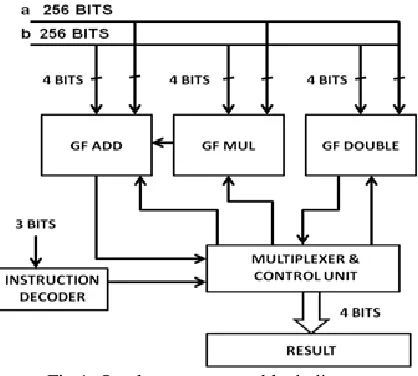
The binary extension unit designed for the polynomial equation p(x)=x4+x+1. Therefore out of
256 input bits 4 bits are taken for the each binary extension unit blocks. The binary extension field unit consists of GF addition, multiplication and double. The binary field addition is designed by using the XOR gate operation. The multiplier unit is designed by the look up table procedure. So this block is consist of memory blocks, which are used for storing the all possible output. The GF double unit consists of a simple addition unit.
Fig 1. Quad core structure block diagram
Fig 2. Block Diagram of Binary Extension field
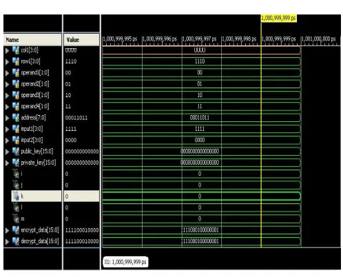
V. SIMULATION RESULT
Fig 3.Simuation Result
VI. RTL SCHEMATIC DIAGRAM
Fig 4. RTL Schematic Diagram
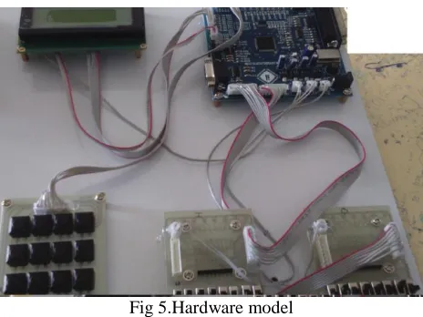
VII. HARDWARE MODEL
Fig 5.Hardware model
FPGA is a semiconductor device that based around a matrix of configurable logic blocks(CLB) connected through programmable interconnects. FPGA can be programmed to the desired application (or) functionality requirements although one-time programmable(OTP) FPGAs are available.
A plane and regular structure in which logic and interconnect both are programmable.
Programmability of logic –any combinational or sequential logic can be implemented.
Programmability of interconnect –any logic component can be connected to anyone else.
Programmable interconnects
Switch box: Connects horizontal channels to vertical channels
Transmission gate (or a pass transistor) is used for each condition.
VIII. CONCLUSION
The quad core structure executes the parallelism with both fields of instructions. At the same time 4 numbers of instructions are executing, this parallelism action will increase the speed. This architecture is an example design of crypto processor for executing prime field and binary field operations. This work has been further developed for the superscalar architecture with more number of instructions.
REFERENCES
[1] Johannes Wolkerstorfer, “Dual-Field Arithmetic Unit for GF(p) and GF(2m)”Institute for Applied Information Processing and Communications, Graz University of Technology, Inffeldgasse 16a, 8010 Graz, Austria. This work origin from the European Commission funded project USB CRYPT established under contractIST-2000-25169 in the Information Society Technologies (IST)Program.
[2] Jun-Hong Chen, Ming-Der Shieh, Member, IEEE, and Wen-Ching Lin, “A High-Performance Unified-Field Reconfigurable Cryptographic Processor” IEEE TRANSACTIONS ON VERY LARGE SCALE INTEGRATION (VLSI) SYSTEMS, VOL. 18, NO. 8, AUGUST 2010.
[3] Michael Grand, Lilian Bossuet2, Guy Gogniat, Bertrand Le Gal, Jean-Philippe Delahaye and Dominique Dallet, “A Reconfigurable Multi-core Cryptoprocessor for Multi-channel Communication Systems”, published in "IPDPS - 25th IEEE International Parallel & Distributed Processing Symposium, Anchorage : United States (2011)"
[4] Santosh Ghosh, Debdeep Mukhopadhyay, and Dipanwita Roychowdhury “Secure Dual-Core Cryptoprocessor for Pairings Over Barreto-Naehrig Curves on FPGA Platform” IEEE TRANSACTIONS ON VERY LARGE SCALE INTEGRATION (VLSI) SYSTEMS,
[5] P.C. Kocher, “Timing attacks on implementations of diffle-hellman, RSA,DSS and other systems,” in Adv. Cryptology-CRYPTO’96,LNCS1109,pp.104-113,1996.
[6] D.Kammler, D.Zhang, P.Schwabe,H. charwaechter, M. Langenberg, D. Auras, G. Ascheid, and R. Mathar, “Designing an ASIP for cryptographic pairings over Barreto-Naehrig Curves,” CHES’09, LNCS 5747, pp. 254-271,2009.
[7] J. Fan, F. Vercauteren, and I.Verbauwhede, “Faster Fp-arithematic for Cryptographic pairings on Barreto-Naehrig curves,” CHES’09, LNCS 5747,
pp.240-253, 2009.
[8] D. N. Amanor, C. Paar, J. Pelzl, V. Bunimov, and M. Schimmler, “Efficient hardware architectures for modular multiplication on FPGAs,” in proc.Int. Conf. Field Program. LogicAppl.,pp.539-542, 2005.
[9] V. Bunimov and M. Schmiller, “Area and time efficient modular multiplication of large integers,” in Proc. ASAP,pp.400-409, 2003.
[10] Huapeng Wu, Member IEEE, “Bit-Parallel Finite Field Multiplier and Squarer Using Polynomial Basis”, IEEE TRANSACTIONS ON COMPUTERS, VOL. 51, NO. 7, JULY 2002