New Controller Strategy for Two Switch Dc
Voltage Regulator
R. Sakthivel, M. Arun
Assistant Professor, Dept. of Electrical Engineering, Annamalai University, Chidambaram, India Assistant Professor, Dept. of Electrical Engineering, Annamalai University, Chidambaram, India
ABSTRACT: For wide voltage range of input change, buck-boost converter is suitable for getting a regulated voltage
in the output (load) side. The single switch buck-boost converter produced as inverting output. So the buck-boost topology is improved with two switches. The two switch buck-boost converter produces a non-inverting dc output. Input voltage feed forward method is used to select the buck or boost mode according to the input voltage level. In this work the two switch buck-boost converter is designed and modeled with different controller [PI,PID&IMC].
In the proposed system,a new control scheme ‘internal model control’ is implemented to compare the performance of the two mode converter. The two mode converter is modeled in the MATLAB environment with PI&PID controllers and as well as internal model control .the system is designed for 12-32V input, 24V output, and 48W-rated power. The entire performance of the buck-boost converter is compared.
I. INTRODUCTION
The role of a DC-DC converter is very important where need a constant DC voltage from a variable DC source like solar, fuel cells, etc. On the other hand get a variable DC voltage from a fixed DC source by using DC-DC converter.
In this paper, the performance of buck-boost converter is analysed. Normally, buck-boost converter consists of single switch to do both the operations buck and boost according to the duty cycle of the gate pulse.Single switch buck-boost converter produces an inverting output with respect to input. This is a disadvantage of this converter.To get a non-inverting output voltage the converter is designed with two switches one for buck operation and another one for boost operation. The two mode control is achieved by implementing the input feed forward method. According to the input voltage level, buck or boost switch is selected.In this work the two switch buck-boost converter is designed to get a constant output of 24V from a varying input voltage of 12-32V. To regulate the output voltage closed loop control is adopted. In the closed loop control PI / PID controller is used to get the desired output voltage.The same converter topology is analysed with “Internal Model Control” and the performance of the various control techniques are compared.
II. LITRATURE SURVEY
1. Design of a Novel Two Switch Non-inverting Buck-Boost Converterbased Maximum Power point Tracking System
(International Journal ofElectrical and Computer Engineering (IJECE), Vol. 3, No. 4, August2013, pp. 467~477, ISSN: 2088-8708).
ability to work over a wide range of input voltage to generate both higher and lower voltages while supplying high current makes this topology an attractive choice. Another advantage of non-inverting buck-boost converter is that it has a capacity for extra current storage in the inductor.
A non-inverting buck-boost converter is used in the MPPT system in this experiment. The P & O method was implemented using PIC16F73, a robust microcontroller.
1.1. Non-Inverting Buck-Boost Converter
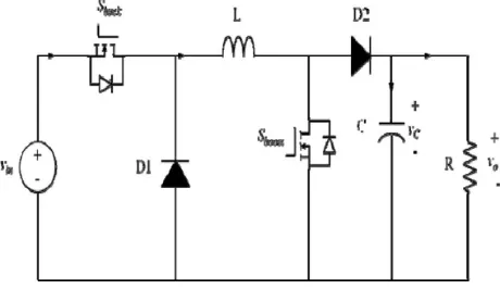
A non-inverting buck-boost converter is essentially a cascaded combination of a buck converter followed by a boost converter, where a single inductor-capacitor is used for both converters. As the name implies, this converter does not invert the polarities of the output voltage in relation to the polarities of the input. This converter requires the use of two active switches and is designed by combining a buck converter and boost converter design in the same topology. Due to this design this converter can work as Buck-only, Boost-only or Buck-Boost converter. The input voltage source is connected in parallel with diode D1, MOSFET Sboost, load capacitor, C. MOSFET Sbuck is connected between the input voltage source and diode D1. The inductor is connected between D1 and Sboost, while D2 is connected between Sboost and the output or load capacitor.
Figure 1.Two switch non-inverting buck-boost converter
2. A New Two Switch Topology Buck Boost Converter In Universal Input PFC Application (International Journal
of Applied Engineering andTechnology ISSN: 2277-212X, 2013 Vol. 3 (2) April-June, pp.13-18 / Khandare et al)
In universal-input PFC applications, the capability of providing both step-up and step-down conversion is attractive because the output dc voltage can be set to any value. However, conventional single-switch buck-boost topologies, including the buck-boost, fly back, SEPIC, and Cuk converters, (Uceda, 1997) have greatly increased component stresses and component sizes compared to the boost converter. In Buck boost converters for power-factor-correction (PFC), the universal-input capability. (Erickson, 2006) In this paper, we propose a new two-switch topology,
boost-interleaved buck-boost (BoIBB) converter, which can offer significant performance. improvements over
single-switch buck-boost converters or other two-single-switch buck-boost converters in universal-input PFC applications. High efficiency (over 93%) throughout the universal-input ac line voltage range is demonstrated on an experimental 100-W, 200-V dc output and universal-input BOIBB PFC rectifier.
V. PROPOSED SYSTEM
1. Introduction
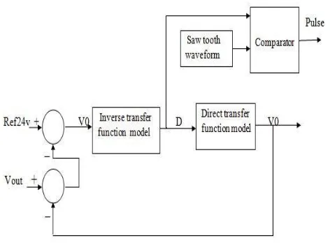
2. Internal Model Control
Internal Model Control (IMC) is a commonly used technique thatprovides a transparent mode for the design
and tuning of various types of control. The ability of proportional-integral (PI) and proportional-integral-derivative (PID) controllers to meet most of the control objectives has led to their widespread acceptance in the control industry. The Internal Model Control (IMC)-based approach for controller design is one of the control technique used in control applications in industries.
As the IMC approach is based on pole zero cancellation, methods which comprise IMC design principles result in a good set point responses. However, the IMC results in a long settling time for the load disturbances for lag dominant processes which are not desirable in the control industry.
Procedure to Design IMC for two mode TSBB converter
Fig. 2 IMC Basic Strategy
In the above figure Qc is the IMC controller. The PI controller is replaced with the IMC. The IMC block consists of the Inverse Model of the process (plant).
Procedure
The system to be controlled is modeled as a transfer function model. The inverse model of the system is derived.
The Inverse model will act as the controller of the process.
The transfer function model is used to tune the system for fast performance.
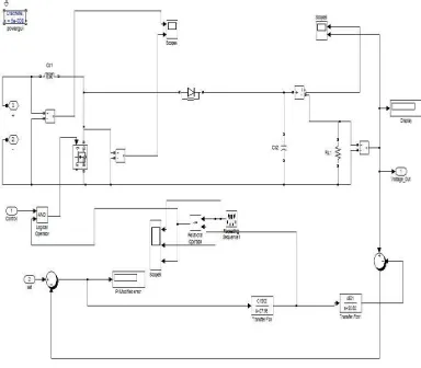
Modelling of the two mode two switch buck-boost converter using IMC controller
The buck and boost converters are designed and constructed individually in matlab2013 environment.
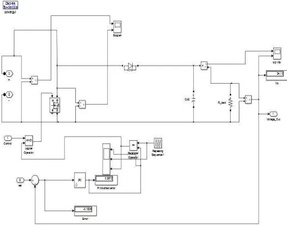
MATLAB simulation model of TSBB DC-DC converter using IMC&PI controller
Figure 3simulation diagram of TSBB converter using IMC&PI controller
MATLAB simulation model of buck subsystem using IMC controller
Figure 5. simulation diagram of boost subsystem using PI controller Simulation Results
TABLE 1Line regulations for TSBB converter using IMC&PI controller
TABLE 2 Load regulationfor TSBB converter using IMC&PI controller.
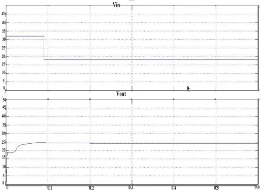
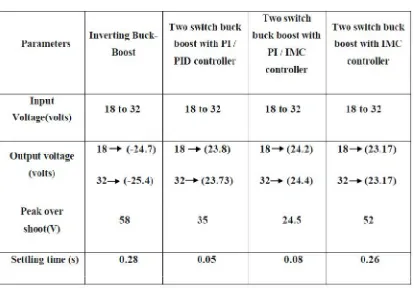
Transient performance Peak overshoot: 24.5V Settling time: 0.08s
Comments on results:
MATLAB simulation model of Two Switch Buck Boost DC-DC Converter using INTERNAL MODEL CONTROL technique.
Figure 7 simulation diagram of TSBB converter using IMC controller.
MATLAB simulation model of Buck subsystem using IMC Controller
MATLAB simulation model of Boost subsystem using IMC Controller
Figure 9. simulation diagram of boost subsystem using IMC controller
Simulation Results
TABLE 3 Line regulation for TSBB converter using IMC controller.
TABLE4 load regulation for TSBB converter using IMC controller.
Transient Performance
Settling time : 0.32s
Peak overshoot : 55V
Comments on Results
From the simulation results, the output of the TSBB converter is non-inverted.
VI. CONCLUSION
In this work, performance of non-inverting two switch buck-boost converter was designed and modelled in MATALB software. Three control techniques (PI, PID and Internal Model Control) are used to regulate the output voltage.
From the simulation results it is concluded that performance of TSBB converter is better than the single switch buck-boost converter in both steady state and transient conditions. Among the control schemes used in two switch converter, the performance of PI & IMC Controller is better in transient conditions but in the point of view of voltage regulation, PI&PID controller is better. According to the application requirement we can select the controller either PI&IMC or PI&PID.
A prototype model of proposed converter with PI/PID control algorithm was developed. The performance of the converter was validated in the laboratory conditions. The working range of the hardware model is 12V to 32V.
REFERENCES
1) C. Wei, C. Chen, K. Wu, and I. Ko, “Design of an average-current-mode non inverting buck-boost dc-dc converter with reduced switching and conduction losses,” IEEE Trans. Power Electron., vol. 27, no. 12, pp. 4934– 4943, Dec. 2012.
2) C. Yao, X. Ruan, and X. Wang, “Isolated buck-boost dc/dc converters suitable for wide input-voltage range,” IEEE Trans. Power Electron., vol. 26, no. 9, pp. 2599–2613, Sep. 2011.
3) D. C. Jones and R. W. Erickson, “A nonlinear state machine for dead zone avoidance and mitigation in a synchronous non inverting buck-boost converter,” IEEE Trans. Power Electron., vol. 28, no. 1, pp. 467–480, Jan. 2013.
4) E. Schaltz, P. O. Rasmussen, and A. Khaligh, “Non-inverting buck-boost converter for fuel cell application,” in Proc. IEEE Annual Conf. IEEE Ind. Electron., 2008, pp. 855–860
5) Improved filter design in internal model control” by C.J.Gombas, R.D.Braatz (1996).
6) J. J. Chen, P. N. Shen, and Y. S. Hwang, “A high efficiency positive buckboost converter with mode-select circuit and feed-forward techniques,” IEEE Trans. Power Electron., vol. 28, no. 9, pp. 4240–4247, Sep. 2013