DEVELOPMENT OF A NON-PULSATING BUCK-BOOST CONVERTER WITH CONTINUOUS CURRENT MODE (CCM)
MOHD SHARIF BIN ZAKARIA
A thesis submitted in
fulfillment of the requirement for the award of the Degree Master of Electrical Engineering
Faculty of Electrical and Electronic Engineering Universiti Tun Hussein Onn Malaysia
ABSTRACT
ABSTRAK
CONTENTS
TITLE i
DECLARATION ii
DEDICATION iii
ACKNOWLEDGEMENT iv
ABSTRACT v
CONTENTS vii
LIST OF TABLES ix
LIST OF FIGURES x
LIST OF SYMBOLS AND ABBREVIATIONS xii
CHAPTER 1 1
1.1 PROJECT BACKGROUND 1
1.2 PROBLEM STATEMENTS 2
1.3 PROJECT OBJECTIVES 3
1.4 PROJECT SCOPES 3
1.5 THESIS OVERVIEW 3
CHAPTER 2 5
2.1 INTRODUCTION 5
2.2 DC-DC CONVERTER 5
2.3 FUNCTION OF DC-DC CONVERTER 6
2.4 DC-DC CONVERTER SWITCHING 7
2.5 THE OPERATION OF BUCK-BOOST CONVERTER 10
2.6 PID CONTROLLER 14
CHAPTER 3 16
3.1 CIRCUIT DIAGRAM 16
3.2 THE CONTROLLER 17
3.3 BUCK CONVERTER 18
3.4.1 CONTINUOUS CONDUCTION MODE 23
3.4.2 DISCONTINUOUS CONDUCTION MODE 24
3.5 BOOST CONVERTER 25
3.6 MODE OF OPERATION 27
3.6.1 CONTINUOUS CONDUCTION MODE 27
3.6.2 DISCONTINUOUS CONDUCTION MODE 29
3.7 DESIGN CONSIDERATIONS 30
CHAPTER 4 32
4.1 INTRODUCTION 32
4.2 CONVERTER WITHOUT FEEDBACK 32
4.3 CONVERTER USING CLOSE LOOP 34
4.4 PERFORMANCE DURING BUCK OPERATION 35
4.5 PERFORMANCE DURING BOOST OPERATION 36
CHAPTER 5 39
5.1 CONCLUSION 39
5.2 FUTURE WORKS 40
LIST OF TABLE
Table 1 : Circuit Parameter 17
Table 2 : Data Input-Output for Converter Without feedback 33
LIST OF FIGURE
Figure 2-1: General DC-DC converter block diagram 6
Figure 2-2 : Switching of DC-DC converter. 7
Figure 2-3 : Switching pulse 8
Figure 2-4 : Continuous Conduction Mode. 9
Figure 2-5 : Discontinuous Conduction Mode. 9
Figure 2-6 : Inductor current and voltage during short circuit. 9
Figure 2-7 : Buck-Boost converter diagram 10
Figure 2-8 : waveforms of buck boost converter 11
Figure 3-1 : Buck Converter Circuit 18
Figure 3-2 : PWM signal to control the switches in the DC-DC converter 19 Figure 3-3 : Equivalent circuit of the buck converter when the switch is closed 20 Figure 3-4 : Equivalent circuit of the buck converter when the switch is open 20 Figure 3-5 : Ideal switch, (a) used to reduce the voltage dc component 21 Figure 3-6 : (b) its output voltage waveform vs(t). 21 Figure 3-7 : Output voltage dc component by the switching period. 22 Figure 3-8 : Insertion of low-pass filter, to remove switching harmonics and pass
only the dc component of vs(t) to the output. 23
Figure 3-9 : Buck converter dc output the voltage V vs. duty cycle D. 23 Figure 3-10 : Inductor current waveform of PWM converter 24
Figure 3-11 : Boost converter. 25
Figure 3-12 : Boost converter when switch S is on. 27 Figure 3-13 : Boost converter when switch S is off. 28 Figure 3-14 : Operating mode waveforms for boost converter in CCM. 29 Figure 3-15 : Boost converter when both switch S and diode D are off. 30
Figure 4-1 : Open Loop selection switch 32
Figure 4-2 : Converter Performance Without feedback System 33
Figure 4-3 : Variation Against Targeted Output 34
Figure 4-5 : Converter Performance 37
LIST OF SYMBOLS AND ABBREVIATIONS
Symbol
v0 Output voltage
vcon Control voltage
Vref Reference voltage
k p , kI Proportional gain and integral gain of P-I controller
k1 Voltage reduction factor
vramp Sawtooth or Ramp voltage
VU ,VL Upper and Lower threshold voltages
q Switching signal
h Switching hypersurface
iref Reference current
C Capacitor
CCM Continuous Conduction Mode ce Change of Error
D Duty Cycle
DC Direct Current
DCM Discontinuous Conduction Mode
e Error
Fs Frequency Switching GUI Graphical User Interface KD Derivative gain
KI Integral gain KP Proportional gain
L Inductor
PID Proportional Integral Derivative PWM Pulse Width Modulation
R Resistor
S Switch
V
C - Voltage (Calculation) V
o - Output Voltage
V
s - Input Voltage
Kth switching cycle V
ref Reference output
CHAPTER 1
INTRODUCTION
1.1 PROJECT BACKGROUND
DC-DC converters are electronic devices used to change DC electrical power efficiently from one voltage level to another. The advantages over AC because DC can simply be stepped up or down. They provide smooth acceleration control, high efficiency, and fast dynamic response. DC converter can be used in regenerative braking of DC motor to return energy back into the supply, and this feature results in energy saving for transportation system with frequent stop; and also are used, in DC voltage regulation.In many ways, a DC-DC converter is the DC equivalent of a transformer. There are FOUR main types of converter usually called the buck, boost, buck-boost and Boost converters. The buck converter is used for voltage step-down/reduction, while the boost converter is used for voltage step-up. The buck-boost and Cuk converters can be used for either step-down or step-up [1].
Controller for the PWM switching control is restraining to Proportional-Integral-Differential (PID) controller. This controller often applied to the converters because of their simplicity. However, implementations of this control method to the nonlinear plants such as the power converters will undergo from dynamic response of the converter output voltage regulation. In general, PID controller produces long rise time when the overshoot in output voltage decreases [2].
Nowadays, the control systems for many power electronic appliances have been increasing widely. Crucial with these demands, many researchers or designers have been struggling to find the most economic and reliable controller to meet these demands. The idea to have a control system in dc-dc converter is to ensure desired voltage output can be produced efficiently as compared to open loop system. [2]
In this project, MATLAB/Simulink is used as a platform in designing the PID logic controller. MATLAB/Simulink simulation model is built to study the dynamic behavior of DC-DC converter and performance of proposed controller.
1.2 PROBLEM STATEMENTS
Buck-Boost DC-DC converters is capable to step-down and step-up the input voltage to produce fixed output voltage. Problem with higher current ripple will influenced and decreased the output voltage regulation and efficiency of the converter.
1.3 PROJECT OBJECTIVES
The objectives of this project are;
i) To model and analyze a DC-DC Buck-Boost converter without controller (open loop) and simulate using MATLAB Simulink.
ii) To design PID Controller to control the switching of DC-DC Buck-Boost Converter and simulate using MATLAB Simulink.
iii) To analyze the voltage output for DC-DC Buck-Boost converter between open loop and PID controller.
1.4 PROJECT SCOPES
The scopes of this project is to simulate the proposed method of voltage tracking of DC-DC buck-boost converter using PID controller with MATLAB Simulink software. Analyses of the converter will be done for improving performance DC-DC buck-bosst converter using PID in continuous current mode (CCM) only.
1.5 THESIS OVERVIEW
This project report is organized as follows;
i) Chapter 1 briefs the overall background of the study. A quick glimpse of study touched in first sub-topic. The heart of study such as problem statement, project objective, and project scope and project report layout is present well through this chapter.
ii) Chapter 2 covers the literature review of previous case study based on PID controller background and development. Besides, general information about Buck-Boost Converter and theoretical revision on CCM mode system also described in this chapter.
iii) Chapter 3 presents the methodology used to design open loop Buck-Boost Converter without and with PID controller. All the components that have been used in designing Buck-Boost Converter are described well in this chapter.
Open loop and PID controller will be analyzed with helps from set of figures and tables.
CHAPTER 2
LITERATUR REVIEW
2.1 INTRODUCTION
The switched mode dc-dc converters are some of the simplest power electronic circuits which convert one level of electrical voltage into another level by switching action. These converters have received an increasing deal of interest in many areas. This is due to their wide applications like power supplies for personal computers, office equipments, appliance control, telecommunication equipments, DC motor drives, automotive, aircraft, etc.
The commonly used control methods for dc-dc converters are pulse width modulated (PWM) voltage mode control, PWM current mode control with proportional (P), proportional integral (PI), and proportional integral derivative (PID) controller. [3]
2.2 DC-DC CONVERTER
In many industrial applications, it is required to convert a fixed-voltage dc source into a variable-voltage dc source. A DC-DC converter converts directly from dc to dc and is simply known as a DC converter. A dc converter can be considered as dc equivalent to an AC transformer with continuously variable turn ratio. Like transformer, it can be used to step down or step up a dc voltage source. (Muhammad H. Rashid, 2004) [1]
energy saving for transportation system with frequent stop; and also are used, in dc voltage regulation. There are many types of DC-DC convertor which is buck (step down) converter, boost (step-up) converter, buck-boost (step up- step-down) convertor. (Muhammad H. Rashid, 1993) [1]
DC conversion is of great importance in many applications, starting from low power applications to high power applications. The goal of any system is to emphasize and achieve the efficiency to meet the system needs and requirements. Several topologies have been developed in this area, but all these topologies can be considered as apart or a combination of the basic topologies which are buck, boost and flyback (Rashid, M. H., 2007) [1]
For low power levels, linear regulators can provide a very high-quality output voltage. For higher power levels, switching regulators are used. Switching regulators use power electronic semiconductor switches in On and Off states.
[image:15.595.185.424.402.537.2]Because there is a small power loss in those states (low voltage across a switch in the on state, zero current through a switch in the off state), switching regulators can achieve high efficiency energy conversion.
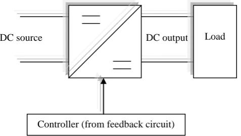
Figure 2-1: General DC-DC converter block diagram
2.3 FUNCTION OF DC-DC CONVERTER
The DC-DC converter has some functions. These are:
i) Convert a DC input voltage Vs into a DC output voltage Vo. ii) Regulate the DC output voltage against load and line variations.
iii) Reduce the AC voltage ripple on the DC output voltage below the required level.
iv) Provide isolation between the input source and the load (if required).
DC output DC source
Controller (from feedback circuit)
v) Protect the supplied system and the input source from electromagnetic interference (Rashid, M. H., 2007) [1]
The DC-DC converter is considered as the heart of the power supply, thus it will affect the overall performance of the power supply system. The converter accepts DC and produces a controlled DC output.
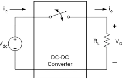
2.4 DC-DC CONVERTER SWITCHING
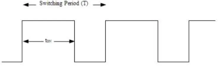
There are two switching condition that need to be applied, that is when ON and OFF as shown in Figure 2-2.
When ON,
Output voltage is the same as the input voltage and the voltage across the switch is 0V.
When OFF,
[image:16.595.211.428.477.624.2]Output voltage = 0V and current through the switch = 0A. In ideal condition, power loss = 0W since output power equal to input power.
Figure 2-2 : Switching of DC-DC converter.
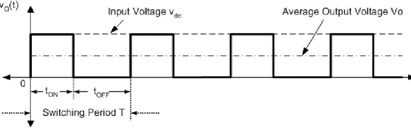
Figure 2-3 : Switching pulse
Thus, duty cycle, D, which depends on tON and range of duty cycle is
0 D 1. If switching frequency, fs, is given,
Average DC output voltage,
There are two modes of operation in DC-DC converters based on inductor current, iL,
i) Continuous Conduction Mode (CCM), when iL 0.
ii) Discontinuous Conduction Mode (DCM) when iL goes to 0 and stays at 0 for
some time. s on on off on on
f
t
T
t
t
t
t
D
(2.1)( )
0
0 0
1
T1
DTo i i
V
v t dt
V dt
V D
T
T
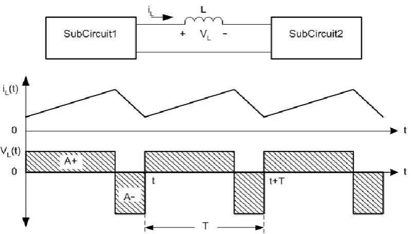
Figure 2-4 : Continuous Conduction Mode.
Figure 2-5 : Discontinuous Conduction Mode.
In steady state and periodic operation, inductor charges and discharges with
avg
[image:18.595.118.518.476.704.2]V DC voltage across inductor in one period = 0. Thus, inductor looks like a short circuit as shown in Figure 2-6.
2.5 THE OPERATION OF BUCK-BOOST CONVERTER
[image:19.595.178.458.227.386.2]A buck-boost converter provides an output voltage that may be less than or greater than the input voltage hence the name „‟buck-boost‟‟; the output voltage polarity is opposite to that of the input voltage. This converter is also known as an inverting regulator. The circuit arrangement of a buck-boost convertor is shown in Figure 2-7.
The circuit operation divided into two modes. During mode 1, transistor Q1 is turned on and diode Dm is reversed biased. The input current, which rises, flows through
inductor L and transistor Q1. During mode 2, transistor Q1 is switched off and the current, which was flowing through inductor L, would flow through L, C, Dm, and
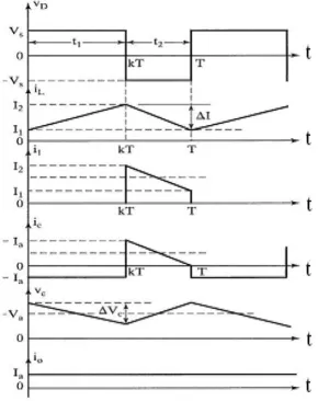
[image:20.595.159.450.268.635.2]the load. The energy stored in inductor L would be transferred to the load and inductor current would fall until transistor Q1 is switched on again in the next cycle. The wave-forms for steady-state voltages and currents of buck boost converter are shown in Figure 2-8
The rate of change of inductor current is a constant, indicating a linearly increasing inductor current. The preceding equation can be expressed as
Δ𝑖𝐿/Δ𝑡=Δ𝑖𝐿/𝐷𝑇=𝑉𝑠/𝐿 (2.3)
Solving for Δ𝑖𝐿 when the switch is closed
(Δ𝑖𝐿)𝑐𝑙𝑜𝑠𝑒𝑑=𝑉𝑠𝐷𝑇/𝐿 (2.4)
Analysis for the switch open.When the switch is open; the current in the inductor cannot change instantly, resulting in a forward-biased diode and current into the resistor and capacitor. In this condition, the voltage across the inductor is
𝑣𝐿=𝑉𝑂=𝐿𝑑𝑖𝐿/𝑑𝑡
𝑑𝑖𝐿/𝑑𝑡=𝑉𝑂/𝐿 (2.5)
Again the rate of change of inductor current is constant, and the change in current is
Δ𝑖𝐿/Δ𝑡 = Δ𝑖𝐿/(1−𝐷)𝑇 = 𝑉0/𝐿 (2.6)
Solving for Δ𝑖𝐿,
(Δ𝑖𝐿)𝑜𝑝𝑒𝑛=𝑉0(1−𝐷)𝑇/𝐿 (2.7)
For steady-state operation, the net change in inductor current must be zero over one period using Eqs.2.2 and 2.5,
(Δ𝑖𝐿)𝑐𝑙𝑜𝑠𝑒𝑑 + (Δ𝑖𝐿)= 0
𝑉𝑠𝐷𝑇/𝐿 + (1−𝐷)/𝐿 = 0 (2.8)
Solving for𝑉𝑂,
Equation 2.7 shows the output voltage has opposite polarity form the source voltage. Output magnitude of the buck boost converter can be less than the source greater than the source, depending on the duty ratio of the switch. If D > 0.5, the output is larger than the input, and if D < 0.5, output is smaller than the input.
Note that the source is never connected directly to the load in the buck boost converter.
Energy is stored in the inductor when the switch is closed and transferred to the load when switch is open. Hence, the buck boost converter is also referred to as an indirect converter.
Power absorbed by the load must be the same as that supplied by the source, Where
𝑃𝑂=𝑃𝑂2/𝑅 (2.10)
𝑃𝑠=𝑉𝑠𝐼𝑆 (2.11)
𝑉𝑂2/𝑅=𝑉𝑆𝐼𝑆 (2.12)
Average source current is related to average inductor current by
𝐼𝑆=𝐼𝐿𝐷
Resulting in
𝑉𝑂2/𝑅=𝑉𝑆𝐼𝐿𝐷 (2.13)
Substituting for 𝑉𝑂 using Eqe 2.7 and solving for
𝐼𝐿= 𝑉𝑂2/V𝑆𝐷𝑅 = 𝑃𝑂/V𝑆𝐷 = 𝑉𝑆𝐷/(1−𝐷)2 (2.14)
Maximum and minimum inductor current is determined using Eqe 2.2 and 2.12
𝐼𝑚𝑎𝑥 = 𝐼𝐿+Δ𝑖𝑙/2 = 𝑉𝑆𝐷/(1−𝐷)2+𝑉𝑆𝐷𝑇/(2𝐿) (2.15)
For continuous current, the inductor current must remain positive. To determine the boundary between continuous and discontinuous current 𝐼𝑚𝑖𝑛 is set to zero in Eqe 2.14,
(𝐿𝐹)𝑚𝑖𝑛 = (1−𝐷)2𝑅/2 (2.17)
Or
𝐿𝑚𝑖𝑛 = (1−𝐷)2𝑅/2𝑓 (2.18)
When F is switching frequency in hertz
Output voltage ripple
The output voltage ripple for the buck boost converter is computed from the capacitor current waveform
│Δ𝑄│ = (𝑉𝑂/𝑅) = 𝐶Δ𝑉𝑂 (2.19)
Solving for Δ𝑉𝑂,
𝑉𝑂 = 𝑉𝑂𝐷𝑇/𝑅𝐶 = 𝑉𝑂𝐷/𝑅𝐶𝐹 (2.20) Δ𝑉𝑂/𝑉𝑂=𝐷/𝑅𝐶𝐹 (2.21)
2.6 PID CONTROLLER
Controllers respond to the error between a selected set point and the offset or error signal that is the difference between the measurement value and the set point. Optimum values can be computed based upon the natural frequency of a system. Too much feedback (positive feedback cause stability problems) causes increasing oscillation [3]. With proportional (gain) only control the output increases or decreases to a new value that is proportional to the error. Higher gain makes the output change larger corresponding to the error. Integral can be added to the proportional action to ramp the output at a particular rate thus bring the error back toward zero. Derivative can be added as a momentary spike of corrective action that tails off. Derivative can be a bad thing with a noisy signal. Typical steps for designing a PID controller are;
i. Determine what characteristics of the system need to be improved. ii. Use KP to decrease the rise time.
CHAPTER 3
METHODOLOGY
[image:25.595.104.528.341.552.2]3.1 CIRCUIT DIAGRAM
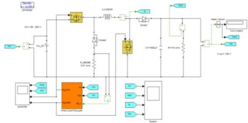
Figure 3-1 Buck-Boost Converter Circuit
Figure 3-1, show the circuit diagram used for simulation using Matlab/Simulink in this projec. Two MOSFET switch used to turn on/off the switching. The MOSFET also act as selector to select operation of converter either Buck Converter or Boost Converter depending on input givent.
Table 1 : Circuit Parameter
No Item Parameter
1 Input Voltage (Vin) 50 – 200V
2 Output Voltage (Vout) 100V ±5%
3 Power (Pout) 1000W
4 Frequency (f) 10kHz
5 Inductor (L) 10 mH
6 Capacitor (Cout) 1000 μF
7 Rsense 0.01 Ω
8 Rsense 10 Ω
3.2 THE CONTROLLER
[image:26.595.120.525.456.730.2]Traditional PWM controller where use switching on/off the MOSFET, may not good enought to perform in the current converter where the application required power converter to respond to demand. Figure 3-2, show the controller used for converter.
3.3 BUCK CONVERTER
The operation of the buck converter is fairly simple, with an inductor and two switches (usually a transistor and a diode) that control the inductor. It alternates between connecting the inductor to source voltage to store energy in the inductor and discharging the inductor into the load.
[image:27.595.116.526.288.470.2]The buck converter, shown in Figure 3-3, converts the unregulated source voltage Vin into a lower output voltage Vout. The NPN transistor shown in Figure 1 works as a switch. The ratio of the ON time ( tON ) when the switch is closed to the entire switching period (T) is defined as the duty cycle D = to/T. The corresponding PWM signal is shown in Figure 3-5 .
[image:27.595.138.507.460.729.2]Figure 3-3 : Buck Converter Circuit
Figure 3-5 : Buck Operation - Voltage and Current Respond
Figure 3-6 : PWM signal to control the switches in the DC-DC converter
[image:28.595.122.493.517.636.2]capacitor supplies energy to the load, and the inductor current flows through the capacitor and the diode [2]. The output voltage is controlled by varying the duty cycle. On steady state, the ratio of output voltage over input voltage is D, given by
[image:29.595.117.419.161.296.2]Vout/ Vin.
Figure 3-7 : Equivalent circuit of the buck converter when the switch is closed
Figure 3-8 : Equivalent circuit of the buck converter when the switch is open
A buck converter is a step-down DC to DC converter. Its design is similar to the step-up boost converter, and like the boost converter it is a switched-mode power supply that uses two switches (a transistor and a diode), an inductor and a capacitor.
The buck converter reducing the dc voltage, using only nondissipative switches, inductors, and capacitors. The switch produces a rectangular waveform
[image:29.595.216.413.372.514.2]transistors and diodes, which are controlled to turn on and off as required to perform the function of the ideal equal to the inverse of the switching period Ts, generally lies in the range of switching speed of the semiconductor devices.
[image:30.595.184.436.229.320.2]The duty ratio D is the fraction of time which the switch spends in position 1, and is a number between zero and one. The complement of the duty ratio, D’, is defined as (1-D) [2].
Figure 3-9 : Ideal switch, (a) used to reduce the voltage dc component
Figure 3-10 : (b) its output voltage waveform vs(t).
The switch reduces the dc component of the voltage: the switch output voltage vs(t) has a dc component which is less than the converter dc input voltage Vg. From Fourier analysis, we know that the dc component of vs(t) is given by its average value <vs>, or
< Vs> =
YVs t dt Ts 0 ( )1
(3.1)
[image:30.595.194.441.396.524.2]<Vs> = DTsVg DVg
Ts( )
1
(3.2)
So the average value, or dc component, of vs(t) is equal to the duty cycle
[image:31.595.197.413.199.282.2]times the dc input voltage Vg. The switch reduces the dc voltage by a factor of D.
Figure 3-11 : Output voltage dc component by the switching period.
What remains is to insert a low-pass filter as shown in Figure 3-12. The filter is designed to pass the dc component of vs(t), but to reject the components of
vs(t) at the switching frequency and its harmonics. The output voltage v(t) is then essentially equal to the dc component of vs(t):
V<Vs>=DVg (3.3)
The converter of Figure 3-11 has been realized using lossless elements. To the extent that they are ideal, the inductor, capacitor, and switch do not dissipate power. For example, when the switch is closed, its voltage drop is zero, and the current is zero when the switch is open. In either case, the power dissipated by the switch is zero. Hence, efficiencies approaching 100% can be obtained. So to the extent that the components are ideal, we can realize our objective of changing dc voltage levels using a lossless network.
The network of Figure 3-12 also allows control of the output. Figure 3-13 is the control characteristic of the converter. The output voltage, given by equation (3.3), is
plotted vs. duty cycle. The buck converter has a linear control characteristic. Also, the output voltage is less than or equal to the input voltage. Feedback
output voltage. Inverters or power amplifiers can also be built, in which the duty cycle varies slowly with time and the output voltage follows [3].
Figure 3-12 : Insertion of low-pass filter, to remove switching harmonics and pass only the dc component of vs(t) to the output.
Figure 3-13 : Buck converter dc output the voltage V vs. duty cycle D.
3.4 MODE OF OPERATION
The operation of dc-dc converters can be classified by the continuity of inductor current flow. So dc-dc converter has two different modes of operation that are
(a) Continuous conduction mode (CCM) and (b) Discontinuous conduction mode (DCM).
A converter can be design in any mode of operation according to the requirement.
3.4.1 CONTINUOUS CONDUCTION MODE
[image:32.595.238.394.296.400.2]shown in figure 2.12(a). The converter operating in CCM delivers larger current than in DCM.
3.4.2 DISCONTINUOUS CONDUCTION MODE
[image:33.595.162.461.289.602.2]When the inductor current has an interval of time staying at zero with no charge and discharge then it is said to be working in Discontinuous Conduction Mode (DCM) operation and the waveform of inductor current is illustrated in figure 3-10(c). At lighter load currents, converter operates in DCM. The regulated output voltage in DCM does not have a linear relationship with the input voltage as in CCM.
Figure 3-14 : Inductor current waveform of PWM converter (a) CCM (b) boundary of CCM and DCM (c) DCM
REFERENCES
[1] H. R. Muhammad, Power Electronics Circuit, Devices and Applications, Florida: Computer Engineering University of West Florida, 2004.
[2] U. R. Mohan, dalam Power Electronics Converter Application and Design, John Wiley & Son, Inc, 2003, pp. 231-303.
[3] J. a. R. L.Guo, “PID Controller Modification to Improve Steady-State Performance of Digital Controller for Buck and Boost Converters,” dalam
Conference Proceeding of IEEE Applied Power Electronics Conference and
Exposition, pp. 381-388, Feb 2002, 2002.
[4] S. H. B. Jamali, “Voltage Tracking of DC-DC Boost Converter Using Gaussian Fuzzy Lofic Controller,” Universiti Tun Hussein Onn Malaysia, Batu Pahat, 2012.
[5] A. S. Weddell, "Photovoltaic Sample-and-Hold Circuit Enabling MPPT Indoors for Low-Power Systems," IEEE TRANSACTIONS ON CIRCUITS AND
SYSTEMS, vol. 59, p. 1196, 6 June 2012.
[6] N. Abd Malek, A. R. Abd Rahman, H. B. Hasini dan M. N. Mohd Jaafar, “An Improved Solar PV System for Malaysian Rural Electrification,” dalam 2010 IEEE Student Conference on Research and Development (SCOReD 2010),, Putrajaya, Malaysia, 2010.
[7] G. Y. a. P. A.Perry, “A New Design Method for PI-Like Fuzzy Logic Controller for DC-DC Converters,” dalam 35th Annual IEEE Power Electronics Specialists Conference, Aache, German, 2004.
[8] M. K. K. T. a. P. S. M. Ahmed, “Implementing Sliding Mode Control for Buck Converter,” dalam IEEE 34th Annual Power Electronics Specialist Conference, Vol. 2, pp. 634-637m June 2003, 2003.
[10] Z. H. G. a. X. Q.Hu, “Application of Sliding Mode Control in Control of Power Electronics Converters,” dalam Proceeding 5th International Conference on Electrical Machines and System, Vol.42, No.2, pp.117-122, April 2001, 2001. [11] Y. a. A. W.Gao, “Discreat-Time variable Structure Control System,” dalam
IEEE Transaction on Industrial Electronics, Vol.42, No.2, pp.117-122, April
1995, 1995.
[12] J. O. a. M. J.Matas, “Discreat Sliding Mode Control of Boost Converter for Output Coltage Tracking,” dalam 8th International Conference on Power Electronics and Variable Speed Drives, pp.351-354, Sep 2000, 2000. [13] L. a. G. P.Mattevelli, “General Purpose Sliding Mode Controller for DC/DC
Converter Application,” dalam 24th Annual IEEE Power Electronics Specialist Conference, pp.609-615, June 1993, 1993.
[14] M. N. M.A, “Voltage Tracking of A DC-DC Converter Using Neural Network Control,” Universiti Tun Hussein Onn Malaysia; Master's Thesis, 2012. [15] S. H. Jamali, “Voltage Tracking of DC-DC Converter Using Gaussian Fuzzy