Int. J. of Engg. Sci. & Mgmt. (IJESM), Vol. 3, Issue 2: April-June: 2013, 101-106
INTERNATIONAL JOURNAL OF ENGINEERING SCIENCES
&
MANAGEMENT
LOW-POWER AND AREA-EFFICIENT CARRY SELECT ADDER V.Hari Prasad*1, Dr. L. Rangaiah2
*1,2
SRIT, Anantapur, India
ABSTRACT
Carry Select Adder (CSLA) is one of the fastest adders used in many data-processing processors to perform fast arithmetic functions. From the structure of the CSLA, it is clear that there is scope for reducing the area and power consumption in the CSLA. This work uses a simple and efficient gate-level modification to significantly reduce the area and power of the CSLA. Based on this modification 8-, 16-, 32-, and 64-b square-root.CSLA (SQRT CSLA) architecture have been developed and compared with the regular SQRT CSLA architecture. The proposed design has reduced area and power as compared with the regular SQRT CSLA with only a slight increase in the delay. This work evaluates the performance of the proposed designs in terms of delay, area, power, and their products by hand with logical effort and through custom design and layout in 0.18- m CMOS process technology. The results analysis shows that the propose. CSLA structure is better than the regular SQRT CSLA.
Keywords: Leadership, Management development, Succession planning
INTRODUCTION
Design of area- and power-efficient high-speed data path logic systems are one of the most substantial areas of research in VLSI system design. In digital adders, the speed of addition is limited by the time required to propagate a carry through the adder. The sum for each bit position in an elementary adder is generated sequentially only after the previous bit position has been summed and a carry propagated into the next position.
Corresponding Author*
Email-
The CSLA is used in many computational systems to alleviate the problem of carry
propagation delay by independently
generating multiple carries and then select a carry to generate the sum [1]. However,the CSLA is not area efficient because it uses multiple pairs of Ripple Carry Adders (RCA) to generate partial sum and carry by considering carry input cin=0 and cin=1, then the final sum and carry are elected by the multiplexers (mux).
Int. J. of Engg. Sci. & Mgmt. (IJESM), Vol. 3, Issue 2: April-June: 2013, 101-106 gates than the n-bit Full Adder (FA)
structure. The details of the BEC logic are discussedin Section III.
This brief is structured as follows. Section II deals with the delay and area evaluation methodology of the basic adder blocks. Section III presents the detailed structure and the function of the BEC logic. The
SQRT CSLA has been chosen for
comparison with the proposed design as it has a more balanced delay, and requires lower power and area [5], [6]. The delay and area evaluation methodology of the regular and modified SQRT CSLA are presented in Sections IV and V, respectively. The ASIC implementation details and results are analyzed in Section VI. Finally, the work is concluded in Section VII.
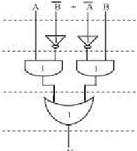
Fig. 1. Delay and Area evaluation of an XOR gate.
Fig. 2. 4-b BEC
Fig. 3. 4-b BEC with 8:4 mux.
DELAY AND AREA EVALUATION
METHODOLOGY OF THE
BASICADDER BLOCKS
The AND, OR, and Inverter (AOI) implementation of an XOR gate is shown in Fig. 1. The gates between the dotted lines are performing the operations in parallel and the numeric representation of each gate indicates the delay contributed by that gate. The delay and area evaluation methodology considers all gates to be made up of AND, OR, and Inverter, each having delay equal to 1 unit and area equal to 1 unit. We then add up the number of gates in the longest path of a logic block that contributes to the maximum delay. The area evaluation is done by counting the total number of AOI gates required for each logic block. Based on this approach, the CSLA adder blocks of 2:1 mux, Half Adder (HA), and FA are evaluated and listed in Table I.
TABLE I DELAY AND AREA COUNT OF THE BASIC BLOCKS OF CSLA
Adder blocks Delay Area
Xor 3 5
2:1 mux 3 4
Half adder 3 6
Full adder 6 13
TABLE II FUNCTION TABLE OF THE 4-b BEC
B[3:0] X[3:0]
0000 0001 .
Int. J. of Engg. Sci. & Mgmt. (IJESM), Vol. 3, Issue 2: April-June: 2013, 101-106 .
. 1110 1111
. . 1111 0000
BEC
As stated above the main idea of this work is to use BEC instead of the RCA with cin=1 in order to reduce the area and power consumption of the regular CSLA. To replace the n-bit RCA, an n+1-bit BEC is required. A structure and the function table of a 4-b BEC are shown in Fig. 2 and Table II, respectively.
Fig. 3 illustrates how the basic function of the CSLA is obtained by using the 4-bit BEC together with the mux. One input of the 8:4 mux gets as it input (B3, B2, B1, and B0) and another input of the mux is the BEC output. This produces the two possible partial results in parallel and the mux is used to select either the BEC output or the direct inputs according to the control signal Cin. The importance of the BEC logic stems from the large silicon area reduction when the CSLA with large number of bits are designed. The Boolean expressions of the 4-bit BEC is listed as (note the functional symbols ~ NOT, & AND ^XOR)
X0= ~B0 X1=B0 ^ B1
X2=B2^ ( B0 &B1) X3=B3^ (B0 &B1 &B2)
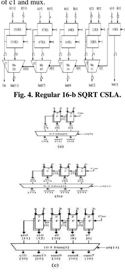
DELAY AND AREA EVALUATION METHODOLOGY OF REGULAR 16-B SQRT CSLA
The structure of the 16-b regular SQRT CSLA is shown in Fig. 4. It has five groups of different size RCA. The delay and area evaluation of each group are shown in Fig. 5, in which the numerals within [] specify the delay values, e.g., sum2 requires 10 gate
delays. The steps leading to the evaluation are as follows.
The group2 [see Fig. 5(a)] has two sets of 2-b RCA. Based on the consideration of delay values of Table I, the arrival time of selection input c1[time[t]=7] of 6:3 mux is
earlier than s3[t=8] and later than
s2[t=6].Thus, sum3[t=6] is summation of s3 and mux[t=3] and sum2[t=10] is summation of c1 and mux.
Int. J. of Engg. Sci. & Mgmt. (IJESM), Vol. 3, Issue 2: April-June: 2013, 101-106 Fig. 5. Delay and area evaluation of regular SQRT
CSLA: (a) group2, (b) group3, (c) group4, and (d) group5. F is a Full Adder
Except for group2, the arrival time of mux selection input is always greater than the arrival time of data outputs from the RCA’s. Thus, the delay of group3 to group5 is determined, respectively as follows:
{C6,sum[6:4]}=c3[t=10]+mux {C10,sum[10:7]}=c6[t=13]+mux Cout,sum[15:11]}=c10[t=16]+mux
The one set of 2-b RCA in group2 has 2 FA for cin=1and the other set has 1 FA and 1 HA for cin=0. Based on the area count
Table lll
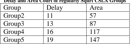
Delay and Area Court of regularly Squrt CSLA Groups
Group Delay Area
Group2 11 57
Group3 13 87
Group4 16 117
Group5 19 147
of Table I, the total number of gate counts in group2 is determined as follows:
Gate court = 57(FA+HA+Mux) FA=39(3*13)
HA=6(1*6) Mux=12(3*4)
Similarly, the estimated maximum delay and area of the other groups in the regular SQRT CSLA are evaluated and listed in Table III.
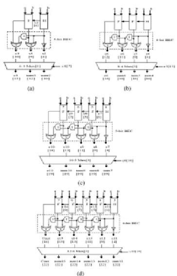
DELAY AND AREA EVALUATION METHODOLOGY OF MODIFIED 16-B SQRT CSLA
The structure of the proposed 16-b SQRT CSLA using BEC for RCA with cin=1 to optimize the area and power is shown in Fig. 6. We again split the structure into five groups. The delay and area estimation of each group are shown in Fig. 7. The steps leading to the evaluation are given here.The group2 [see Fig. 7(a)] has one 2-b RCA which has 1 FA and 1 HA for cin=0. Instead of another 2-b RCA with cin=1 a 3-b BEC is used which adds one to the output from 2-b RCA. Based on the consideration of delay values of Table I, the arrival time of selection input c1[time(t)=7] of 6:3 mux is earlier than the s3[t=9] and c3[t=10] and later than the s2[t=4]. Thus, the sum3 and final c3(output from mux) are depending on s3and mux and partial c3 (input to mux) and mux, respectively. The sum2 depends on c1 and mux. For the remaining group’s the arrival time of mux selection input is always greater than the arrival time of data inputs from the BEC’s. Thus, the delay of the remaining groups depends on the arrival time of mux selection input and the mux delay.
Int. J. of Engg. Sci. & Mgmt. (IJESM), Vol. 3, Issue 2: April-June: 2013, 101-106
Fig 7:Delay and area evaluation of modified SQRT CSLA : (a)group2, (b)
group3,(c)group4,(d)group5,H is a Half Adder.
The area count of group2 is determined as follows:
Gate count= 43(FA + HA + Mux + BEC) FA = 13(1 * 13)
HA = 6(1 * 6) AND = 1 NOT = 1
XOR = 10 (2 * 5) Mux = 12(3*4)
Similarly, the estimated maximum delay and area of the other groups of the modified SQRT CSLA are evaluated and listed in
Table IV. Comparing Tables III and IV, it is clear that the proposed modified SQRT CSLA saves 113 gate areas than the regular SQRT CSLA, with only 11 increases in gate delays..
FPGA IMPLEMENTATION RESULTS The design proposed in MA-CSLA is successfully tested using (Xilinx) Spartan 3E series target and verilog HDL. The MA-CSLA architecture is simulated using isimulator. The result analysis of Modified CSLA ( M-CSLA) and Modified Area efficient CSLA(MA-CSLA) is compared below
Fig Simulation Result
Fig Simulation Result
CONCLUSION
Int. J. of Engg. Sci. & Mgmt. (IJESM), Vol. 3, Issue 2: April-June: 2013, 101-106 of the 64-b modified SQRT CSLA are
significantly reduced by 17.4% and 15.4% respectively. The power-delay product and also the area-delay product of the proposed design show a decrease for 16-, 32-, and 64-b sizes which indicates the success of the method and not a mere tradeoff of delay for power and area. The modified CSLA architecture is therefore, low area, low power, simple and efficient for VLSI hardware implementation. It would be interesting to test the design of the modified 128-b SQRT CSLA.
REFERENCES:
[1] O. J. Bedrij, “Carry-select adder,”
IRE Trans. Electron. Comput., pp.
340–344, 1962.
[2] B. Ramkumar, H.M. Kittur, and P. M. Kannan, “ASIC implementation of modified faster carry save adder,”
Eur. J. Sci. Res., vol. 42, no. 1, pp.
53–58, 2010.
[3] T. Y. Ceiang and M. J. Hsiao, “Carry-select adder using single ripple carry adder,” Electron. Lett., vol. 34, no. 22, pp. 2101–2103, Oct. 1998.
[4] Y. Kim and L.-S. Kim, “64-bit carry-select adder with reduced area,”
Electron. Lett., vol. 37, no. 10, pp.
614–615, May 2001.
[5] J. M. Rabaey, Digtal Integrated
Circuits—A Design
Perspective.Upper Saddle River, NJ:
Prentice-Hall, 2001.
[6] Y. He, C. H. Chang, and J. Gu, “An area efficient 64-bit square root carry-select adder for lowpower applications,” in Proc. IEEE Int.
Symp. Circuits Syst., 2005, vol. 4,
pp. 4082–4085.