Design of Compact EBG Structure and
effect on Circularly Polarized Triangular
Patch with Stub
Snehalata Chokat, M. Tech. Student
Pune Institute of Computer Technology, Pune-411043 Email:[email protected]
Raj Kumar
DIAT (DU), Girinagar, Pune-411025,India Email: [email protected]
Abstract
This paper presents the study of electromagnetic band gap (EBG) structure using slot ring and its effect on circularly polarized triangular patch antenna performance. The EBG structure has been designed on dielectric substrate εr=4.3 and thickness h=1.53mm. The EBG structure acts as resonator which attenuates the surface wave propagation in a specific frequency range. A new single slot ring EBG structure is proposed which exhibits surface wave attenuation better than 20 dB in the frequency range from 2.75 GHz to 3.2 GHz. An antenna with center frequency of 2.8 GHz is designed with and without EBG. The peak gain and radiation efficiency of this antenna are improved significantly when antenna is above EBG in comparison to antenna without EBG. The simulated radiation patterns of the antenna exhibit reduction in backward radiation when antenna above EBG plane in comparison to radiation pattern without EBG.
Keywords- Electromagnetic band gap (EBG), periodic structures, fractal geometry, platting through hole (PTH), microstrip antenna, and surface wave suppression.
1. Introduction
Electromagnetic band gap terminology is based on the photonic band gap phenomena in optics that are realized by Periodical structures [1]. Electromagnetic band gap structures are revealed in two ways, the suppression of surface wave propagation and in-phase reflection coefficient. The uniqueness of surface wave suppression is to improve antenna performance such as increase in antenna gain, bandwidth and reduction in back radiation
.
structure i.e. mushroom type EBG structure [6] to improve the antenna performance. The EBG structure has also proposed for improving the microwave circuit performamce [7]. Some have proposed compact EBG structure [8] to reduce the overall size of antenna.
In this paper, a new electromagnetic band gap structure is proposed to suppress the surface wave in specific frequency range. Then, a triangular patch antenna is designed using this EBG structure to overcome the undesirable features due to surface waves. The antenna performance is evaluated using EBG structure in term of gain, bandwidth, radiation efficiency and radiation patterns.
2. Basic EBG Structure
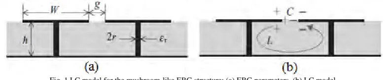
To understand the operation mechanism of EBG structures, some circuit models have been discussed. We consider a simple two-dimensional planar electromagnetic band gap (EBG) structure as shown in Figure 1. The EBG structure consists of four parts which are: 1) A ground plane; 2) A dielectric substrate; 3) connecting vias; 4) metallic patches. Vertical via’s connecting the patches and ground plane. This geometry is called mushroom type structure. The parameters of the EBG structure are labeled in Figure 1(a) as patch width W, gap between the patches is g, substrate thickness h, dielectric constant and vias radius r. When the periodicity (W + g) is small compared to the operating wavelength, the operation mechanism of this EBG structure can be explained using an effective medium model with equivalent lumped LC elements, as shown in Figure 1(b). The capacitance is due to the gap between the patches and the inductance is due to the current along adjacent patches. The impedance of a parallel resonant LC circuit is given by:
(1)
(2) Where: Z = Impedance of a parallel resonant circuit, L = Inductance of resonant circuit, C = Capacitance of resonant circuit, ω = Operating frequency, ωo= Resonant frequency.
The value of the capacitor is given by the fringing capacitance between neighboring coplanar metal plates. This can be derived using conformal mapping, a common technique for determining two-dimensional electrostatic field distributions. The derivation starts with a pair of semi-infinite plates separated by a gap and then truncates them with a finite patch size. Finally, the edge capacitance for the narrow gap situation is given by the following equation:
(3)
The value of the inductor is derived from the current loop in Figure 1 (b), consisting of via and metal sheets. For a solenoid current, the magnetic field can be calculated using Ampere’s law. The equivalent inductor is then computed from the stored magnetic field energy and the excitation current.
Fig. 1LC model for the mushroom-like EBG structure: (a) EBG parameters (b) LC model
The equation of inductance is expressed as below, which depends only on the thickness of the structure and the permeability:
L=µh (4)
ensures that a plane wave will be reflected without the phase reversal that occurs on perfect electric conductor (PEC).
3. Analysis of Simple Mushroom Type EBG
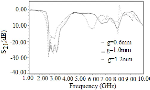
The initial shape of EBG structure has been taken as simple square patch of dimension 8mm × 8mm .This is shown in the Figure 2. The structure comprises with 5 row by 5coloum matrix periodic lattice as shown in the Figure 3. The EBG structure has been designed on FR4 substrate of dielectric constant =4.3 and thickness h=1.53 mm with PTH radius=0.3 mm. On another substrate of same thickness and dielectric constant, a 50 Ω line is placed so as to simulate the EBG performance. The EBG structure metal portions and 50 Ω line are represented in white color as shown in Figure 2. The structure is simulated using Ansoft HFSS electromagnetic simulator software. A comparative graph of simulated results is as shown in the Figure 3. The gap between the patches is varied as g=0.6mm, 1mm, 1.2mm while patch width d is kept constant. The simulated insertion loss S21|dB against frequency is as shown in the Figure 3. We observe that the first band gap is from 2.4 GHz to 3 GHz with gap g=0.6mm, when the gap width g=1mm the band gap is observed from frequency 2.6GHz to 3.5 GHz. When the gap width is further increased there is not much variation in the band gap.
Fig 2 (a) Simple musahroom type EBG, (b) Simple mushroom type EBG structure with 5row x 5coloum, (c) 50Ω microstrip line to analysis EBG performance
Fig. 3 comparative graph of insertion loss for varying gap width of mushroom type of EBG structure
4. Single Slot Ring Type EBG
Fig.4 (a) EBG structure with single slot ring, (b) slot ring EBG structure in 5row x 5 coloum
Fig. 5 comparative graph of insertion loss for various patch width for single slot ring EBG structure
5. Design of Triangular Patch Antenna with Resonating Stub
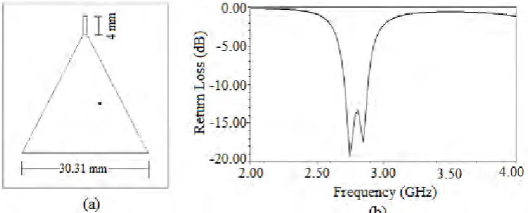
Triangular patch antenna is designed on substrate of dielectric constant =4.3 , height h=1.53mm with stub that connect at an edge of the triangular patch whose length is 4mm. The stub is used to obtain the circular polarization of antenna. The antenna is excited by a coaxial probe and the feed position is located at point shown in the Figure 6a. The patch is an equilateral triangular with 30.31mm side length .The simulated reflection loss S11 in dB of this structure is shown in Figure 6b. The patch antenna operates in the frequency band 2.75 GHz to 2.85 GHz at center frequency of 2.8 GHz.
6. Triangular patch with single slot ring type of EBG
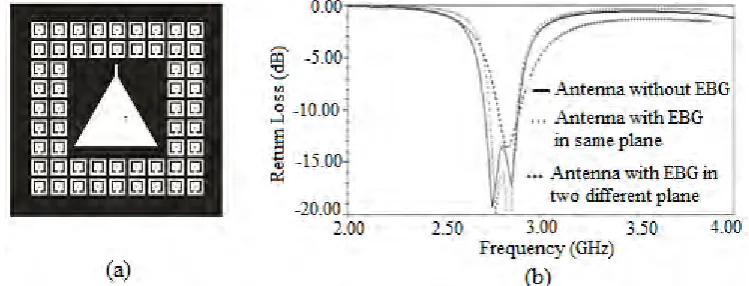
The design of the patch antenna with EBG structure has been done. Initially, the patch is placed in the same plane as the EBG structure as shown in Figure 7a. The patch is placed at the centre of EBG structure. The patch is fed with coaxial feed as in the case of conventional patch antenna. In order to have further gain improvement, the patch is placed above the EBG. This is done by placing an additional substrate into the structure. A comparative graph of return loss for conventional triangular patch, patch with EBG in the same plain and patch and EBG in two different plane is shown in the Figure 7b.
Fig. 7(a) Triangular patch with single slot ring type of EBG in the same plane, (b) Simulated return loss of antenna without EBG, with EBG and antenna in same plane and EBG and antenna in different plane
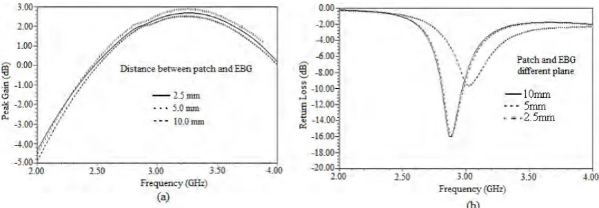
Figure 7b reveals that the circular polarized triangular patch suppresses the surface wave with the introduction of single slot ring type of EBG when EBG and patch are kept in thesame plane. Fig. 8a shows the simulated results of different gap between the patch and EBG. It is observed a shift at higher frequency side as gap between patch and EBG increases. Very small shift is observed when gap between patch and EBG is 5 mm and 10 mm. The simulated axial ratio is also calculated from various gap between patch and EBG as shown in Fig. 8b. It is observed as gap between antenna and EBG increases the axial ratio becomes better. The peak gain of antenna is also calculated for various gap between patch and EBG as shown in Fig. 9a. It is observed from the simulated results the peak gain in better for gap between antenna and EBG 5.0mm at center frequency. The antenna is also simulated for double substrate with gap between EBG and antenna 2.5mm, 5.0mm and 10mm as shown in Fig. 9b. There is a shift when gap between patch and antenna increases upto 5mm. Beyond 5mm the shift is negligible as shown in Fig. 9b. But the triangular patch antenna losses its circular polarizationwhen the patchis levitated by introducing an additional substrate into the structure.
Fig. 9(a) Simulated peak gain in dB for various gap between antenna and EBG in same plane at gap 2.5mm, 5.0mm and 10mm, (b) Simulated results for various gap between antenna and EBG in different plane at gap 2.5mm, 5.0mm and 10mm
The peak gain of antenna is also simulated for antenna without EBG, antenna and EBG in same plane and antenna over EBG structure. The simulated peak gain (dB) versus frequency for all the three cases are shown in Figure 10a. It is observed the peak gain for all the three cases at center frequency is higher in comparison to other frequencies. It is also observed the peak gain is higher when the antenna and EBG both are in different plane. The gain in this case improved by 2 dB in comparison to antenna and EBG in same plane and gain around 3.5 dB improved in comparison to antenna without EBG. The radiation efficiency of antenna for all the cases i.e antenna without EBG, antenna and EBG in same plane and antenna and EBG in different plane. The comparison of all three are shown in Figure 10b. It is observed that radiation efficiency is better around 70% at center frequency when antenna and EBG in different plane. The radiation efficiency of antenna and EBG in same is better at higher frequency in comparison to antenna without EBG but less than when antenna and EBG in different plane.
Fig.10 (a) Simulated comparison of gain for antenna without EBG, antenna and EBG in same plane and antenna and EBG in different plane, (b) Simulated comparison of radiation efficiency for antenna without EBG, antenna and EBG in same plane and antenna and EBG in different plane
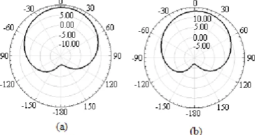
Fig. 11, Radiation Pattern of antenna with single substrate a)2.5mm gap between antenna and EBG (b) 5mm gap between EBG and antenna (c)10mm gap between EBG and antenna
Fig. 12 Simulated Radiation pattern without EBG Simulated radiation pattern with EBG and patch in two different plane when gap between EBG and antenna 2.5mm
7. Conclusions
This paper presents a novel EBG structure along with the triangular patch antenna. The simulated results reveal that with implementation of EBG structure to microstrip patch antenna improves in the gain as well as directivity of the antenna. The EBG structures attenuates the surface wave in frequency range from 2.75 GHz to 3.2 GHz better than 20 dB. In this band, a triangular patch antenna with stub is designed. The gain and efficiency
improvement of antenna are obtained. The good radiation characteristics of the antenna with EBG is achieved with
back radiation reduction. Peak gain of triangular patch antenna without EBG is approximately 0.8 dB which is enhanced to 2.6dB with the implementation of EBG structure, thus leading to an increase in gain up to 1.8 dB. Such type of antenna can be useful for portable communication system.
References
[1] E.Y ablonovitch (1987): Inhibited spontaneous emission in solid state physics and electronics, Physics Review Letters, vol. 58, 2059– 63, 1987.
[2] Y. Rahmat-Samii and H.Mosallaei (2001): Electromagnetic bandgap structures: classification, characterization and applications, Proceedings of IEE-ICAP symposium, pp. 560–4 .
[3] Sievenpiper et al.(1999): High-Impedance Surfaces with a Forbidden Frequency Band” IEEE transactions on microwave theory and techniques, vol. 47, no. 11.
[4] F.Yang and Y. Rahmat-Samii (2003): Reflection phase characterizations of the EBG ground plane for low profile wire antenna applications, IEEE Trans. Antennas Propagation., vol. 51, no. 10, 2691–703.
[5] C. R. Simovski, P. Maagt, and I. V. Melchakova (2005): High impedance surfaces having resonance with respect to polarization and incident angle,” IEEE Trans. Antennas Propagat., vol. 53, no. 3, 908–14.
[6] F. Yang and Y. Rahmat-Samii (2001): A low profile polarized curl antenna over electromagnetic band-gap (EBG) surface,” Microwave Optical Tech. Lett., vol. 31, no. 4, 264–7.
[7] F.-R. Yang, K.-P. Ma, Y. Qian, and T. Itoh (1999): A novel TEM waveguide using uniplanar compact photonic-bandgap (UC-PBG) structure,” IEEE Trans Microwave Theory Tech., vol. 47,no. 11, 2092–8.