University of Pennsylvania
ScholarlyCommons
Publicly Accessible Penn Dissertations
1-1-2013
Interrogation of Single Asperity Electrical Contacts
Using atomic force Microscopy With Application
to Nems Logic Switches
Graham E. Wabiszewski
University of Pennsylvania, [email protected]
Follow this and additional works at:
http://repository.upenn.edu/edissertations
Part of the
Electrical and Electronics Commons
, and the
Mechanical Engineering Commons
This paper is posted at ScholarlyCommons.http://repository.upenn.edu/edissertations/935
For more information, please [email protected].
Recommended Citation
Wabiszewski, Graham E., "Interrogation of Single Asperity Electrical Contacts Using atomic force Microscopy With Application to Nems Logic Switches" (2013).Publicly Accessible Penn Dissertations. 935.
Interrogation of Single Asperity Electrical Contacts Using atomic force
Microscopy With Application to Nems Logic Switches
Abstract
Energy consumption by computers and electronics is currently 15% of worldwide energy output, and
growing. Aggressive scaling of the fully-electronic transistor, which is the fundamental computational element of these devices, has led to significant and immutable energy losses. Ohmic nanoelectromechanical systems (NEMS) logic switches have been recognized as a potential transistor replacement technology with projected energy savings of one to three orders of magnitude over traditional, fully-electronic transistors. However, the use of conventional, adhesive contact materials (i.e. metals) in NEMS switches electrical contacts leads to permanent device seizure or the formation of insulating tribofilms that inhibits commercialization of this technology. Of critical need is a method to efficiently identify and interrogate low adhesion, chemically stable electrical contact material pairs under conditions and scales relevant to NEMS logic switch contacts. This thesis presents the development of two electrical contact testing methods based on atomic force microscopy (AFM) to interrogate electrical contact materials under contact forces and environments representative of NEMS logic switch operating conditions. AFM was used to mimic the interaction of Pt/Pt NEMS logic switch electrical interfaces for up to two billion contact cycles in laboratory timeframes. Contact resistance before cycling significantly exceeded theoretical predictions for clean Pt/Pt interfaces due to adsorbed contaminant films and increased up to six orders of magnitude due to cycling-induced insulating tribopolymer growth. Sliding of the contact with microscale amplitudes lead to significant recovery of conductivity through displacement of the insulating films. Based on this observation, AFM was then used to investigate the role of load, shear, electrical bias, and environment on the electrical robustness of Pt/nitrogen-incorporated ultrananocrystalline diamond (N-UNCD) and Pt/Pt interfaces. N-UNCD was selected because similar diamond films have demonstrated low adhesion, chemical inertness, and compatibility with NEMS logic device fabrication. Pt/N-UNCD interfaces subjected to low loads during sliding demonstrated significant increases in contact resistance due to insulating film formation that was not observed at larger loads. Taken in concert, these finding demonstrate the capability of AFM to investigate nanoscale electrical contact
phenomena without the need for time-consuming and expensive integration of unproven materials in NEMS logic switches.
Degree Type
Dissertation
Degree Name
Doctor of Philosophy (PhD)
Graduate Group
Mechanical Engineering & Applied Mechanics
First Advisor
Second Advisor
Gianluca Piazza
Keywords
Atomic force microscopy, Electrical contacts, Nanoelectromechanical systems, Tribology, Tribopolymer
Subject Categories
INTERROGATION OF SINGLE ASPERITY ELECTRICAL CONTACTS USING
ATOMIC FORCE MICROSCOPY WITH APPLICATION TO NEMS LOGIC
SWITCHES
Graham E. Wabiszewski
A DISSERTATION
in
Mechanical Engineering and Applied Mechanics
Presented to the Faculties of the University of Pennsylvania
in
Partial Fulfillment of the Requirements for the
Degree of Doctor of Philosophy
2013
Supervisor of Dissertation Co-supervisor of Dissertation
________________________________ ________________________________ Robert W. Carpick, Professor and Chair of Gianluca Piazza, Associate Professor of
Mechanical Engineering and Applied Mechanics Electrical and Computer Engineering,
Carnegie Mellon University
Graduate Group Chairperson
________________________________
Jennifer R. Lukes, Associate Professor and Graduate Group Chair of Mechanical Engineering and Applied Mechanics
Dissertation Committee:
John L. Bassani, Richard H. and S.L. Gabel Professor of Mechanical Engineering and Applied Mechanics
INTERROGATION OF SINGLE ASPERITY ELECTRICAL CONTACTS USING
ATOMIC FORCE MICROSCOPY WITH APPLICATION TO NEMS LOGIC
SWITCHES
COPYRIGHT
2013
iv
ACKNOWLEDGMENTS
Thank you, first and foremost, to my advisors, Professor Robert W. Carpick and
Professor Gianluca Piazza. Your guidance, patience, and direction have helped me immensely
over the course of my graduate education and research.
Thank you, Rob, for taking me under your wing. You have been a great friend, mentor,
and advocate. You have shown me, through example, how to be a scientist and engineer. Your
positivity and love for engineering is infectious. I am forever indebted to you.
I would also like to thank my committee members, Professor John Bassani and Professor
Daniel Gianola, for their time, input, and help over the course of my graduate studies.
While the work presented in this thesis bears the name of a single author, none of it
would have been possible without the support and help of many individuals. I would like to thank
Dr. Augusto Tazzoli for his help in creating the logarithmic current amplifier that enabled the
majority of the work presented here. I would like to thank Dr. Andrew Konicek for his PEEM work,
revisions on my written work, and endless encouragement. I thank Dr. Anirudha Sumant for the
growth of N-UNCD and useful discussions. I thank Frank Streller for his consistent review of my
work, help with fabrication and instrumentation, and useful discussions. I would like to thank Dr.
Filippo Mangolini for his help with XPS measurements and guidance. I thank Dr. Tevis Jacobs,
Alex Goodman, and Peter Rockett for their work on the design and fabrication of the TEM
multiprobe holder. I also thank Dr. Nipun Sinha for performing many Pt and Au film depositions
that enabled the development of the methodologies presented in this thesis.
Many other individuals have contributed heavily to the work described in this thesis. I
would like to thank Dr. Vahid Vahdat, Dr. Erin Flater, Dr. David Grierson, Dr. Qunyang Li, and Dr.
Christian Greiner for helpful, useful, and interesting discussions. I would like to thank Peter
Szczesniak for his willingness to machine anything in a pinch. I thank Maryeileen Banford Griffith,
Olivia Brubaker, Susan Waddington Pilder, and Desirae Johnson for their help with administrative
Funding from DARPA grant MIPR 06-W238 for the development of low power
piezoactuated NEMS logic, phase III program is acknowledged.
Use of the University of Pennsylvania Nano/Bio Interface instrumentation is
acknowledged.
Use of the facilities of the Pennsylvania Regional Nanotechnology Facility is
acknowledged.
Use of the Center for Nanoscale Materials was supported by the U.S. Department of
Energy, Office of Science, Office of Basic Energy Sciences, under Contract No.
DE-AC02-06CH11357.
vi ABSTRACT
INTERROGATION OF SINGLE ASPERITY ELECTRICAL CONTACTS USING ATOMIC
FORCE MICROSCOPY WITH APPLICATION TO NEMS LOGIC SWITCHES
Graham E. Wabiszewski
Professor Robert W. Carpick
Professor Gianluca Piazza
Energy consumption by computers and electronics is currently 15% of worldwide energy
output, and growing. Aggressive scaling of the fully-electronic transistor, which is the fundamental
computational element of these devices, has led to significant and immutable energy losses.
Ohmic nanoelectromechanical systems (NEMS) logic switches have been recognized as a
potential transistor replacement technology with projected energy savings of one to three orders
of magnitude over traditional, fully-electronic transistors. However, the use of conventional,
adhesive contact materials (i.e. metals) in NEMS switches electrical contacts leads to permanent
device seizure or the formation of insulating tribofilms that inhibits commercialization of this
technology. Of critical need is a method to efficiently identify and interrogate low adhesion,
chemically stable electrical contact material pairs under conditions and scales relevant to NEMS
logic switch contacts. This thesis presents the development of two electrical contact testing
methods based on atomic force microscopy (AFM) to interrogate electrical contact materials
under contact forces and environments representative of NEMS logic switch operating conditions.
AFM was used to mimic the interaction of Pt/Pt NEMS logic switch electrical interfaces for up to
two billion contact cycles in laboratory timeframes. Contact resistance before cycling significantly
exceeded theoretical predictions for clean Pt/Pt interfaces due to adsorbed contaminant films and
increased up to six orders of magnitude due to cycling-induced insulating tribopolymer growth.
through displacement of the insulating films. Based on this observation, AFM was then used to
investigate the role of load, shear, electrical bias, and environment on the electrical robustness of
Pt/nitrogen-incorporated ultrananocrystalline diamond (N-UNCD) and Pt/Pt interfaces. N-UNCD
was selected because similar diamond films have demonstrated low adhesion, chemical
inertness, and compatibility with NEMS logic device fabrication. Pt/N-UNCD interfaces subjected
to low loads during sliding demonstrated significant increases in contact resistance due to
insulating film formation that was not observed at larger loads. Taken in concert, these finding
demonstrate the capability of AFM to investigate nanoscale electrical contact phenomena without
the need for time-consuming and expensive integration of unproven materials in NEMS logic
viii
TABLE OF CONTENTS
ACKNOWLEDGMENTS ... III
ABSTRACT ... VI
LIST OF TABLES ... XI
LIST OF FIGURES ... XII
CHAPTER 1: INTRODUCTION ... 1
1.1 The Need for Low Power Computation ... 2
1.2 NEMS Switches as an Alternative to the Transistor ... 3
1.3 The Nanoscale Electrical Contact is the Achilles Heel of NEMS Logic Switches ... 8
1.4 Scaling Down: The Operational Requirements of NEMS Logic Switches with Comparison to MEMS Switches ... 10
1.5 Existing Methods to Test Electrical Contact Reliability at the Microscale and the Need for a New Nanoscale Electrical Contact Test Method ... 13
CHAPTER 2: EXPERIMENTAL METHODS ... 16
2.1 Atomic Force Microscopy with Application to Nanoscale Electrical Contacts ... 16
2.1.1 Atomic Force Microscopy as Enabling Instrumentation for Electrical Contact Characterization ... 17
2.1.2 Descriptions of AFMs Used in This Thesis ... 20
2.1.3 Static and Dynamic AFM ... 20
2.1.4 Calibrating AFM Stiffness for Static AFM... 24
2.1.5 Quantifying Peak Interaction Force and Stress during Dynamic AFM ... 27
2.2 Current Amplification during Atomic Force Microscopy ... 37
2.3 Observing the Cantilever Probe Tip Shape ... 38
2.4 Observing the Chemical State of Electrical Contact Surfaces using Chemical Spectroscopy ... 41
2.4.1 XPS Spectroscopy to Interrogate Surface Chemical Composition of Platinum Films ... 42
2.4.2 PEEM Spectromicroscopy to Interrogate the Surface Chemical Composition of Conductive Diamond Films ... 43
2.5.1 Sputtering of Platinum films ... 45
2.5.2 MPECVD Deposition of Nitrogen-incorporated Ultrananocrystalline Diamond ... 45
2.6 Method for the Gigacycle Interrogation of Single Asperity Electrical Contacts Using Atomic Force Microscopy ... 46
2.6.1 Detailed Single Asperity Cycling Test Protocol ... 47
2.6.2 Removal of Insulating Films via Shear Displacement of the Contacts ... 56
2.6.3 Selection of Cantilever Stiffness and Shear Displacement during Cycling ... 56
3.6.4 Materials Investigated ... 60
2.6.5 Method to Investigate the Effect of Voltage and Environment on Nanoscale Electrical Contact Lifetime ... 61
2.6.6 Chemical Interrogation of Platinum Surfaces using X-ray Photoelectron Spectroscopy .. 62
2.7 Overview: Method for the Evaluation of Nitrogen-incorporated Ultrananocrystalline Diamond and Platinum Exposed to Load, Shear, and Electrical Bias ... 63
2.7.1 Protocol for the Evaluation of Nitrogen-incorporated Ultrananocrystalline Diamond and Platinum Exposed to Load, Shear, and Electrical Bias ... 63
2.7.2 Interrogation of Chemical changes to N-UNCD ... 69
CHAPTER 3: RESULTS AND DISCUSSION FOR THE GIGACYCLE TESTING
OF PLATINUM/PLATINUM ELECTRICAL CONTACTS USING ATOMIC
FORCE MICROSCOPY ... 71
3.1 Overview: Contact Cycling Experiments over Several Billion Cycles Using AFM ... 71
3.2 Assessing the Conductivity of Single Asperity Contacts... 71
3.3 The Effect of Voltage during Cycling on Single Asperity Platinum/Platinum Contact Lifetime ... 76
3.3.1 Contact Forces, Contact Stresses, and Contact Time during Cycling ... 77
3.3.2 The Effect of Cycling on Resistance and Adhesion and the Initial Chemical State of the Contact Interface ... 80
3.3.3 Probe Tip Profiles Before and After Cycling and Evidence of Tribopolymer Formation ... 88
3.4 The Effect of Environment and Voltage on Platinum/Platinum Contact Lifetime ... 93
3.4.1 Peak Contact Forces, Peak Contact Stresses, and Contact Time during Cycling ... 95
3.4.2 The Effect of Environment and Voltage on Resistance and Adhesion during Nanoscale Platinum/Platinum Contact Cycling ... 98
3.5 Degradation Mechanisms of Nanoscale Platinum/Platinum Contacts ... 106
3.6 Comparison of Single Asperity Results to Multiasperity Systems ... 108
3.7 Contact Regeneration under Shear Loading ... 110
3.8 Final Remarks ... 113
x
4.1 Overview: The Effect of Load, Shear, and Electrical Bias on Pt/Pt and Pt/Nitrogen-incorporated Ultrananocrystalline Diamond Contacts ... 114 4.2 Current Response of Platinum/Platinum and Platinum/Nitrogen-incorporated
Ultrananocrystalline Diamond Interfaces Subject to ≤50 nN Normal Load, Shear, and Voltage in Laboratory Air and Nitrogen Purged Environments ... 114 4.3 Friction and Current Response of Platinum/Nitrogen-incorporated Ultrananocrystalline Diamond Interfaces Exposed to ≥50 nN Normal Load, Shear, and Electrical Bias in
Humidified Nitrogen and Nitrogen Purged Environments ... 127
CHAPTER 5: CONCLUSIONS AND OPPORTUNITIES ... 138
5.1 Conclusions: Gigacycle Testing of Single Asperity Platinum/Platinum Contacts using Atomic Force Microscopy ... 139 5.2 Conclusions: Subjecting Nitrogen-incorporated Ultrananocrystalline Diamond and Platinum to Load, Shear, and Electrical Bias ... 145 5.3 Future Work and Opportunities ... 147
LIST OF TABLES
Table 1.1: Comparison of the operational requirements of MEMS RF switches vs. NEMS logic switches………...12
Table 2.1: Comparison of the two protocols used in the cycling of nanoscale electrical contacts for up to 2 billion cycles. Protocol 1 (P1) was used to investigate the contact from a few cycles up to several billion cycles. Protocol 2 (P2) focused on 106 – 109 interaction cycles. The number of points during the periodic evaluation of interface conductivity and adhesion was increased substantially from P1 to P2 in order to improve the statistical interpretation of data………...49
Table 2.2: The contact materials, tip-surface voltages, and environment for various single asperity electrical contact cycling tests performed using the AFM-based gigacycle test method. Pt/Pt interfaces were investigated for all tests...62
Table 3.1: The modification bias, radii before and after cycling, and stresses during FvD and dAFM cycling for test series A. Peak normal stresses were calculated using DMT contact
mechanics and the contact forces are compared in figure 3.4...77
Table 3.2: The test identifier name, environment during testing, tip-surface voltage during cycling, final radius, and peak forces and stresses during dAFM cycling for measurement series B through E cycled using protocol P2. Peak normal stresses are calculated using DMT contact mechanics and force ranges are taken from the results plotted in figure 3.13...96
Table 4.1: Test identifier, counter surface material, modification voltage range, environment, and scan load during modification and probing scans for series M measurements. A new Pt-coated AFM probe and surface location were investigated for each test...116
xii
LIST OF FIGURES
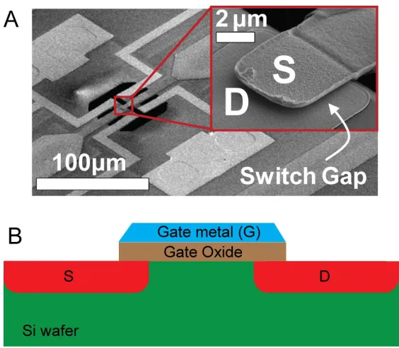
Figure 1.1: (A) Scanning electron microscope image of a prototype piezoelectric ohmic NEMS switch courtesy of Nipun Sinha, University of Pennsylvania. (Inset) Expanded view of the source and drain of the NEMS switch showing the presence of an air gap, (B) Cross-section of an FET (conventional transistor) identifying elements common to both NEMS switches and the FET. The source, drain, and gate structures are labeled, S, D, and G, respectively...4
Figure 1.2: Voltage-current (I-V) plot comparing ohmic NEMS switch, CMOS, and ideal switch performance. The gate voltage, VG, is used to turn the device on resulting in current flow from source to drain. The higher sub-threshold slope of NEMS switch technology allows for the use of lower control voltages that reduce device power consumption per switching event...6
Figure 1.3: Separation force of electrical contacts of various work of adhesion ranges, W, as a function of the number of simultaneously interacting surface asperities. The adhesive interaction of the asperity is treated with DMT contact mechanics (eq. 2.8). Microscale MEMS contacts involve several to hundreds of contacting asperities while the ultimate limit of a NEMS contact is the single asperity. The adhesive force of nanoscale electrical contacts exceeds the restoring force of the actuator for small devices. NEMS logic switch contact materials favor low adhesion in order to limit stiction...9
Figure 1.4: Contact resistance as a function of make/break cycles for microscale noble metal electrical contacts of Au and Pt from various sources. The formation of insulating TP results in a dramatic increase in contact resistance after a critical number of cycles. The use of highly
adhesive contact materials can also lead to stiction of the switch...10
Figure 1.5: Surfaces, even those that are highly polished and smooth to the eye demonstrate nanoscale roughness. (A) A 2 x 2 μm2 atomic force microscopy scan of a smooth Pt surface with a mirror-like finish. (B) A two-dimensional cross section from (A) shows significant nanoscale roughness. (C) A single asperity from the two-dimensional cross-section from (B). The work in this thesis focuses on single asperity surface interactions that represent the fundamental unit of contact of a rough surface or the ultimate limit of contact size for NEMS logic switches...11
Figure 2.1: A general schematic of the working components of a typical conductive AFM setup. The components that confer the core functionality of an AFM are labeled here. This diagram includes a DC voltage source, current amplifier, and series resistor utilized for conductive
AFM...18
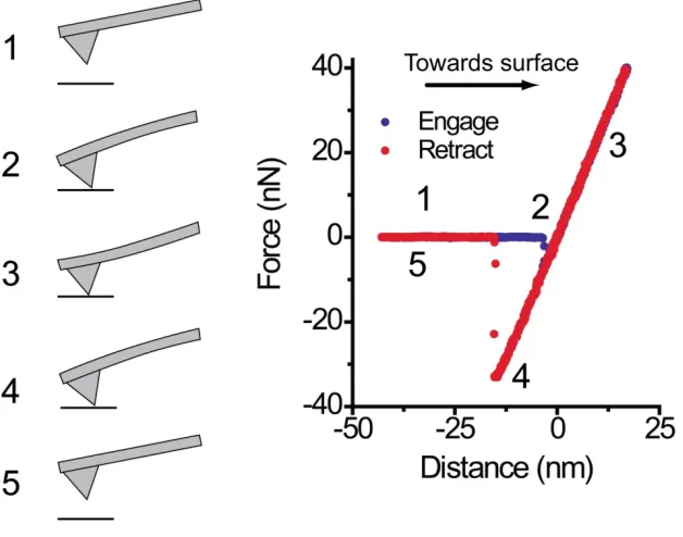
Figure 2.2: A force versus distance (FvD) measurement obtained with a Pt-coated AFM probe on a Pt surface. (Left) A vignette showing a magnified representation of cantilever-sample interaction during an FvD measurement and (right) the FvD data. Relevant interactions are labeled 1 – 5. (1) The probe starts in a retracted state from the surface and the relative tip-sample distance is decreased until snap-in occurs (2). External loads are applied (3) up to a load or distance
specified by the user. The probe is then retracted from the surface. Hysteresis during unloading is due to adhesive interactions between the tip and sample. Pull off (4) occurs when the bending force of the cantilever exceeds to interaction force of the tip and sample. (5) Retraction is
continued until the tip is free from the surface...22
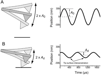
surface to ensure negligible tip-surface interaction forces. (B) The relative tip-sample separation is then decreased until tip-surface forces cause a reduction in the probe amplitude, resulting in damped amplitude Ad. Both the driving signal and the cantilever deflection profile are sinusoidal. Proper selection of A0 and Ad ensures that interpenetrating tip-surface interaction will occur at the trough of the cantilever response...23
Figure 2.4: (A) The tip-surface interaction during dAFM is described using a single degree of freedom harmonic oscillator model. (B) Tip-surface interaction under the appropriate selection of cantilever stiffness, A0, and Ad results in interpenetrating interaction at the trough of the cantilever response that mimics asperity interaction in a nanoscale electrical switch contact...28
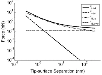
Figure 2.5: Contribution to tip-surface and cantilever-surface loading force in the presence of a voltage applied between the tip and surface. The total interaction force, Ftotal, interaction force due to vdw components, Fvdw, electrostatic tip-surface force, FE,t-s, and electrostatic cantilever-surface force, FE,lever, are included. The plot uses parameters reasonable for testing performed in this thesis with R = 25 nm, θ = 19˚, α = 11˚, L = 225 μm, w = 30 μm, ht = 14.8 μm, H = 1x10-19 J, and a tip-surface voltage of 2 V. The plot shows that voltage applied between the tip and surface leads an additional and non-negligible electrostatic tip-surface interaction force...29
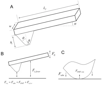
Figure 2.6: (A) Relevant cantilever dimensions used for modeling tip-surface force interaction during dAFM electrical contact cycling. The cantilever tilt angle, α, is 11˚ for the Asylum MFP-3D used in electrical contact cycling. The set of possible, generalized tip-surface, cantilever-surface, and driving force interactions in (B) the out of contact and (C) interpenetrating tip-surface states. (C) Focuses on the tip-surface interaction, which includes both vdw and repulsive DMT
interaction forces, but for visualization purposes does not show the electrostatic cantilever
interactions that exist in the persistent electrostatic (PE) solution described below...33
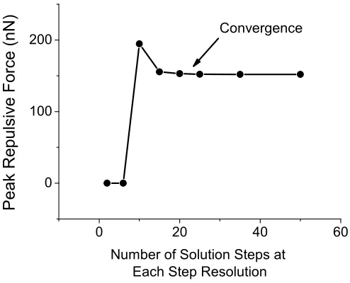
Figure 2.7: Convergence of Ad for tip-surface interaction modeled in Matlab for tip-surface
interaction parameters corresponding to measurement D1 in section 3.4.1...37
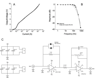
Figure 2.8: (A) Plot of the current-voltage transfer for a custom built-logarithmic amplifier used in this thesis and (B) a bode gain plot of the amplifier response using a 500 MΩ test resister, (C) and a schematic of the logarithmic amplifier circuit...38
Figure 2.9: (A) Side profile of a Pt-coated AFM probe, (B) an expanded view of the tip shank, and (C) a high-resolution TEM micrograph of the probe tip apex. The angle of the probe tip profile (A) is measured to determine the orientation of the probe tip with respect to the contact surface during AFM. These images are corrected for the probe tip profile as it would make contact with a counter surface in AFM...39
Figure 2.10: The protocol used to cycle and interrogate the conductivity and adhesion of
nanoscale electrical contacts. (A) Details of the testing process from start to finish. Steps specific to protocol P1 (left), protocol P2 (right), and both protocols (center) are identified. (B) Details of the cycling and interrogation steps. The tip-surface contact is cycled at high speed and cycling stopped periodically to perform a low frequency evaluation of tip-surface conductivity and
adhesion...49
xiv
used for testing in protocol P2 was taken from the first, stable observation of φ < 90˚ for approximately 0.2<Ar<0.8. This A0 value was then increased by 150% to ensure hard tapping mode interaction for the duration of dAFM cycling...52
Figure 2.12: The relative location of cycling and conductivity and adhesion evaluations. dAFM cycling (red) was performed across a 1 x 1 μm2 window for protocol P2 and at the center of the test region (green circle) for protocol P1. Slow FvD interrogation measurements (black circles) were performed for both protocols P1 and P2. This representation shows 25 FvD measurements. However, up to 1156 FvD regularly spaced measurements were conducted during protocol P2. Lateral scanning of the test area (blue region) was performed before cycling during protocol P2... ...53
Figure 2.13: Interaction force as a function of AFM probe stiffness is subject to AFM system and lateral displacement constraints. Ranges of cantilever stiffness corresponding to various
commercially produced probe styles are listed on the x axis. The requirements of both static AFM and dAFM measurements instruct the necessary probe stiffness for measurements that replicate NEMS switch contacts. The minimum noise floor of an AFM probe due to thermal fluctuations,
Ft,min, is far below the interaction forces required to simulate NEMS contacts. While noise due to mechanical and electrical systems of the AFM, Fnoise, is more appreciable than thermal noise, it does not limit the type of probe used. For investigations of electrical interfaces with forces from 10 to 100 nN the capability to produce tip-surface interactions using dAFM at reasonable cantilever oscillation amplitudes and the desire to restrict lateral sliding/shear during tip-surface interaction bounds the range of probe stiffness that may be used. The yellow area corresponds to the range of forces investigated and probe stiffness used in this work. For Ft,min, Kcant was fixed to 0.2, 2.8, and 42 nN/nm for contact, force modulation, and tapping cantilever types, respectively. ∆ω was conservatively taken to be 100 kHz. A0 was fixed to 400 nm for the dAFM limit and parameters reasonable for the Pt/Pt contacts demonstrated in this study were used (R=50 nm, Et=Es=130 GPa, νt=νs=0.3, Q=200, and Ar=0.58). δnoise was estimated from measurements of noise on the MFP-3D used in experiments presented here and is taken to be 0.5 nm...59
Figure 2.14: The AFM protocol used for evaluating changes to surface conductivity of N-UNCD and Pt exposed to load, shear, and electrical bias. Scans were performed at a new location for each probing scan and modification scan group. A total of i locations were scanned. Probing scans were performed before and after each modification scan to check electrical integrity of the probe tip. A total number of j modification scans are performed at each modification
location...65
Figure 2.15: The relative location of probing and modification scans when testing the effect of load, shear, and electrical bias for Pt and N-UNCD contacts. A probing scan to evaluate the tip conductivity was performed before each group of modification scans. Scan locations are offset by 1 μm from one-another so that resultant tribofilms do not spread between test locations. The voltage during scanning is indicated at each location as the probing voltage, Vp, or the modification voltage at the ith test location, Vm,i. The tests terminated with a final probing
scan...67
Figure 3.1: (Bottom) Force versus distance (FvD) and (top) current versus distance (IvD) measurements for a Pt-coated AFM probe on a Pt surface at a location of high conductivity. The probe was brought into (blue) and out of (red) contact with the surface and force (bottom) and current (top) were measured simultaneously. The snap-in and pulloff instabilities are both evident. The pulloff force (lowest force measurement) was used as measure of the adhesion of this Pt/Pt interface. These measurements were collected at an engage/retraction speed of 100
Figure 3.2: Various distributions of conductivity at maximum load observed during protocol P2 testing of contacts. Data skewed towards (A) low currents, (B) high currents, and (C) with a log-normal distribution have all been observed. In all cases, the mean and median of the data is often separated by several orders of magnitude. In (A), conductivity below the noise floor of the current amplifier (<40 pA) results in significant data with negative current values and leads to significant divergence between the mean and median values. All distribution shown here are composed of 1156 FvD/IvD measurements...74
Figure 3.3: An ensemble of contacts in (A) a MEMS device with N parallel conducting contacts of radius R and (B) N number of NEMS devices with single asperity contacts of radius R...76
Figure 3.4: (Top) Peak force and (bottom) peak normal stress during dAFM cycling for
measurements series A cycled using protocol P1. All calculations are based on average probe radii shown in table 3.1 and work of adhesion described in figure 3.11. Solutions for vdw-only (green), persistent electrostatic (blue), and non-persistent electrostatic (red) tip-surface
interactions are shown for tip-surface conditions after 100 cycles (initial) and 2x10⁹+ cycles (final). These solutions assume Et=Es=130 GPa, νt=νs=0.3, a0=0.2 nm, Ar = 0.57. A0 and Kcant as
measured experimentally. Only tip-surface (modification) voltages above 1 V have a significant effect on the peak tip-surface interaction force...79
Figure 3.5: Average resistance at maximum FvD load as a function of number of tip-surface interaction cycles for data series A collected using protocol P1. Data for low modification voltage,
Vm, is shown on the left and high Vm on the right. The vertical scales for the left and right plots are the same. Each data point represents the average of 25 regularly-spaced FvD/IvD measurements for a total of 350 measurements for each curve. Each data series was collected with a new Pt-coated probe tip at a new Pt surface location...81
Figure 3.6: Mean, lower quartile, and upper quartile current at maximum FvD load as a function of number of tip-surface interaction cycles for data series A collected using protocol P1. All
measurements have been separated into individual plots for clarity. Points below the y-axis range indicate negative currents that were below the noise floor of the logarithmic current
amplifier...82
Figure 3.7: The magnitude of resistance increase as measured at maximum FvD load for data series A collected using protocol P1. The initial contact resistance, Ri, is taken from conductivity measured after 100 contact cycles and final contact resistance, Rf, from conductivity measured at the end of the test (~2x10⁹ cycles)...83 Figure 3.8: (Left) Carbon 1s and (right) oxygen 1s spectra of as deposited and Pirahna cleaned Pt surfaces obtained via XPS...84
Figure 3.9: Average force of adhesion as a function of number of tip-surface interaction cycles for data series A collected using protocol P1. The error bars indicate the standard deviation of 25 measurements at each point for a total of 350 measurements for each curve. Significant
xvi
Figure 3.11: Probe tip profiles obtained by TEM for measurement series A cycled with protocol P1. (Left) Before and (right) after cycling for ~2x10⁹ cycles. The tip-surface voltage during cycling (probing voltage) is listed on the left. All scale bars are the same. Gross changes to tip shape were only observed for A5 and A6 (Vm = 2 V)...89 Figure 3.12: (A) Probe tip profile from series A measurement A1. High resolution image of the contact point (B) and (C) after cycling for 2x10⁹ cycles with Vm=100 mV. Additional low density material appeared in the contact zone. The edge of the original tip profile and the added material are indicated by a yellow and blue dashed line, respectively, in (C)...91
Figure 3.13: (Top) Peak force and (bottom) peak normal stress at the end of dAFM cycling for measurements series B through E cycled using protocol P2. All calculations are based on average probe radii shown in table 3.2 and work of adhesion shown in figure 3.19. Solutions for vdw-only (green), persistent electrostatic (blue), and non-persistent electrostatic (red) tip-surface interactions are shown. Electrostatic solutions are not shown for tests performed under
mechanical cycling. These solutions assume Et=Es=130 GPa, νt=νs=0.3, a0=0.2 nm, Ar = 0.25. Kcant was measured experimentally via thermal calibration...97
Figure 3.14: Average resistance measured from probing FvDs at maximum load (40 nN) for cycling in various environments (N2 purged and laboratory air) and voltage between tip and sample (0 V, mechanical cycling, and 1 V, hot switching). Each data point represents the average of 1156 regularly-spaced FvD measurements collected over a 1 x 1 μm2 surface region. The tip-surface probing voltage, Vp, for all measurements was 200 mV. Each curve represents a new probe at a new Pt surface location...98
Figure 3.15: The magnitude of resistance increase as measured at maximum FvD load for data series B through E collected using protocol P2. Initial contact resistance, Ri, is taken from conductivity measured after ~105 contact cycles and final contact resistance, Rf, from
conductivity measured at the end of the test (~1x10⁹ cycles)...99 Figure 3.16: Relationship between conductivity histograms (left) and heat map histograms (right). (Left) Histograms with a logarithmic conductivity ranges were constructed from conductivity measured at maximum load during engage (40 nN) for FvD/IvD probing measurements before cycling and at various time points during cycling. The bottom histogram represents the distribution of surface conductivity measured before cycling while the top histogram represents the
distribution after 1.3 billion contact cycles. (Right) Heat maps represent histogram distributions as a function of the number of tip-surface interactions. Each horizontal row of the heat map
represents a single conductivity distribution with the color representing the frequency of points within each bin range. The bottom row represents the distribution before cycling and the top row represents the distribution after test completion (~1.3 billion cycles). The lowest current
represented on the heat map is 40 pA, which corresponds to the noise floor of the logarithmic current amplifier...101
Figure 3.17 Histogram heat maps for measurement series B through E cycled using protocol P2. Current is taken from conductivity measured at maximum FvD/IvD load of 40 nN. The heat maps show a recession of the current front with continued cycling that reflects resistance increases observed during cycling. A shift in conductivity from lower to higher currents from the first to second row (0 cycles to ~105 cycles) demonstrates a cleaning of the contact or evolution of the interface geometry due to cycling...102
switching) using protocol P2 for data series B through E. The data sets and colors used in this plot correspond to those used in figure 3.14. Error bars correspond to the standard deviation of 1156 regularly-spaced FvD measurements collected over the same 1 x 1 μm2 surface
region...104
Figure 3.19: Work of adhesion measured at the end of testing (after ~109 cycles) for test series B through E cycled with protocol P2. The probe tip radii used to extract the work of adhesion from the force of adhesion were calculated from TEM profiles after cycling and are listed in table 3.2...105
Figure 3.20: Height profiles of (A) the Pt counter surface used during cycling for series A measurements and (B) series B through E measurements. Pt surfaces in (A) were deposited on glass cover slides that resulted in higher film roughness. Both scans were performed over a 500 x 500 nm2 region while collecting 256 x 256 data points. First order line fits were applied to both sets of data...105
Figure 3.21: Degradation mechanisms observed for single asperity Pt/Pt interfaces cycled under mechanical and hot switching. (A) Adsorbed organic contaminants (C and 0) of ~1.3
nm-thickness were present on the Pt surfaces due to exposure to laboratory air. (B) Initial cycling of the contact resulted in removal of adsorbed material and/or broadening of the contact area that resulted in increased conducitivity. (C) Continued cycling of the contact under low to moderate voltages resulted in growth of TP and an increase in contact resistance. (D) Cycling under moderate voltages lead to periods of TP formation and periodic loss or breakdown of TP resulting in decreased contact resistance. (E) High electrical power during cycling resulted in gross
changes to tip shape and, in one case, lower contact resistance attributed to the exposure of a cleaner Pt interface. Continued cycling of the probe resulted in eventual formation of TP and an increase in contact resistance...107
Figure 3.22: (Left) Change in resistance as a function of contact cycles and (right) absolute resistance as a function of cycles for (left axis) the data obtained by Chen et al. for multiasperity Pt/Pt contact and (right axis) single asperity Pt/Pt contacts investigated here. The change in resistance (right) is of similar magnitude for multiasperity and single asperity contacts. However, initial resistance of both contacts differs by ~104 for multiasperity vs. single asperity
tests...109
Figure 3.23: The current distribution measured at a maximum contact force of 40 nN from 1156 FvD/IvD measurements taken before contact cycling, after contact cycling for ~109 cycles, and after the application of load, shear, and electrical bias to the probe tip C1. A significant
improvement in tip-surface conductivity is observed after applying shear to the contact...111
Figure 3.24: The current distribution measured at a contact force of 15 nN for lateral scanning of a Pt surface (shear loading) and 1156 FvD/IvD measurements taken without applying shear (normal loading). All measurements were taken before cycling of the contact interface and with a tip-sample bias of 200 mV. Current measured during shear scanning of the interface
demonstrates lower average contact resistance...112
xviii
The histogram peak that appears at ~40x10-11 A for both the first and final scan represents low current noise contributions from the current amplifier that dominate during high contact
resistance...117
Figure 4.2: (Top) Median, upper quartile, and lower quartile current from data measured during repeated scanning of 1 x 1 μm2 regions of N-UNCD with a Pt-coated AFM probe at a load of 50 nN in laboratory air (measurement M1). 10 independent locations were scanned for seven passes under load, shear, and electrical bias with increasing modification voltage, Vm, at each new location. Conductivity of the interface decreased with continued scanning at each given location, and conductivity was progressively reduced overall at higher Vm. The lack of lower quartile data (blue line) for Vm = 6.0 V (location 9) occurred because the lower quartile data was below zero (within the noise floor of the amplifier) and cannot be represented on a logarithmic y-axis. (Bottom) Conductivity of the probe tip-surface interface was evaluated before each modification scan and after all tests were completed by scanning previously untested regions of the film near the modification regions in order to check the electrical integrity of the probe tip. The voltage during all probing scans, Vp, was 1 V, load was 50 nN, scan rate was 0.2 Hz, and 64 scan lines and 1024 scan points were collected. Each probing location number identifies the tip integrity evaluation scan performed before the modification scan of the same location number. For instance, probing location one was measured next to (but not intersecting) modification scan location one before data for modification scan location one was collected...119
Figure 4.3: (Top) Median, upper quartile, and lower quartile current from data measured during repeated scanning of 1 x 1 μm2 regions of N-UNCD with a Pt-coated AFM probe at a load of 50 nN in an N2 purged environment for measurement M12. 10 independent locations were scanned under load, shear, and bias for 7 scans each with increasing modification voltage, Vm, at each new location. Conductivity of the interface decreased with continued scanning at each given location, and conductivity was progressively reduced overall at higher Vm. However, unlike in air, the conductivity did not show an overall decrease with applied bias until 3.0 V was applied, at which point a large decrease was observed, which continued at subsequent voltages. (Bottom) Conductivity of the probe tip-surface interface was evaluated before each modification scan and after all tests were completed by scanning previously untested regions of the film near the modification regions in order to check the electrical integrity of the probe tip. The voltage during all probing scans, Vp, was 1 V, load was 50 nN, scan rate was 0.2 Hz, and 64 scan lines and 1024 scan points were collected. Each probing location number identifies the tip integrity evaluation scan performed before the modification scan of the same location number. For instance, probing location one was measured next to (but not intersecting) modification scan location one before data for modification scan location one was collected...120
Figure 4.4: Median change in current from surface current maps measured from the initial scan to the present scan as a function of median power during the initial scan for scanning in an N2 purged environment (blue) and laboratory air (red). Under comparable load, shear, and electrical power, scanning in laboratory air leads to larger changes in conductivity than in N2...123
Figure 4.6: (Left) Trace-retrace friction and (right) current measured during the probing scan of measurement N6 with a Pt-coated AFM probe tip on N-UNCD. The modified region located at the center of the image (brightly colored in the current map) was scanned under an initial load of 50 nN that drifted to 117 nN at the end of testing in a N2 purged environment. Friction decreased and conductivity increased due to load, shear, and electrical power through the contact...130
Figure 4.7: Friction force (uncalibrated, but on the same scale for all measurements) in the modified and unmodified regions for tests N1 through N8. Most tests demonstrated a decrease in friction after modification...131
Figure 4.8: Change in current as a function of change in friction for tests N1 through N8. The color of the data point indicates the relative humidity during testing and the size of the data point represents the magnitude of Vm...132 Figure 4.9: (Left axis) Trace-retrace friction averaged for each scan line and (right axis) current during surface modification scanning with Vm = 10 V with relative humidity >33% RH. (Top) Current persisted during scanning and (bottom) loss of the probe tip due to wear, fracture, or melting resulted in a sudden loss of current. The linear current amplifier was set to high sensitivity during modification scans in order to observe these events, which resulted saturation of the current signal during low resistance tip-surface interaction...133
Figure 4.10: C1s NEXAFS data from inside the modified contact region for scans performed with Vm = 10 V and relative humidity from <4 – 45% RH with comparison to an unmodified region. (Blue) Scans in which current persisted during modification and probing scans, (red) scans resulting loss of the Pt probe tip during modification scans, and (black) an unmodified region of N-UNCD are shown. (Inset) The full carbon edge as measured by PEEM...134
Figure 4.11: O1s NEXAFS data from inside the modified contact region for scans performed with Vm = 10 V and relative humidity from <4 – 45% RH with comparison to an unmodified region. (Blue) Scans in which current persisted during modification and probing scans, (red) scans resulting loss of the Pt probe tip during modification scans, and (black) an unmodified region of N-UNCD are shown...135
Figure 4.12: N1s NEXAFS data from inside the modified contact region for scans performed with Vm = 10 V and relative humidity from <4 – 45% RH with comparison to an unmodified region. (Blue) Scans in which current persisted during modification and probing scans, (red) scans resulting loss of the Pt probe tip during modification scans, and (black) an unmodified region of N-UNCD are shown...136
1
CHAPTER 1: INTRODUCTION
Nanoelectromechanical systems (NEMS) switches have been identified as a potential
next-generation transistor [1] with far lower power consumption than existing electronic integrated
circuits [2], a critical technological need. These switches are nanoscale moving devices that
convert an electrical input signal into motion to close a conductive contact [3]. NEMS switches are
therefore a mechanical version of a transistor with topologies that often mimic larger
microelectromechanical systems (MEMS) switches. However, NEMS switches require small
dimensions for the fast, competitive switching speeds (<100 ns) desired in computer logic
applications. The nanoscale dimensions and complex operating conditions at the electrical
contact make NEMS logic switches susceptible to tribologically-mediated failure mechanisms that
currently render the technology commercially unviable. In particular, the low contact and restoring
forces of NEMS switches may lead to device “stiction” (device permanently stuck closed), or
intolerable increases in switch contact resistance due to the formation of insulating tribopolymer
(TP) films. It may be possible to overcome these problems with the integration of contact
materials that demonstrate low adhesion and resist the formation of insulating TPs. To find
suitable contact materials, different contact material candidates are usually tested by fabricating a
N/MEMS device and testing its reliability - a very time consuming process. There is significant
need to find an efficient way to test different M/NEMS contact material candidates without costly
device fabrication.
This thesis details the development of an electrical contact testing method using atomic force
microscopy (AFM) to evaluate the robustness and adhesion of nanoscale electrical contacts.
Pt/Pt contacts, an electrical interface commonly used for micro- and nanoscale switches, were
cycled for up to two billion interactions using this method. Cycling was performed in a variety of
environments that represent potential operating environments of NEMS logic electrical contact
changes to adhesion, and changes to contact resistance. Transmission electron microscopy
(TEM) was then used to observe the formation of insulating low density materials, referred to here
as TP, at the contact interface.
It is then shown that the application of shear loading of the nanoscale electrical contact
removes insulating TP resulting from contact cycling – a potential actuation mechanism that could
be integrated into NEMS switch design to improve electrical performance. AFM and chemical
spectroscopy were then used to evaluate changes to the conductivity and chemistry of
nitrogen-incorporated ultrananocrystalline diamond, a potential next-generation, nanomechanical switch
contact material, and compared to that of Pt interfaces under load, shear, and electrical bias.
1.1 The Need for Low Power Computation
Sustained growth in computing power in conjunction with a decrease in computing cost has
led to the proliferation of devices utilizing integrated processors in the last half century. These
integrated processors are overwhelmingly based on fully-electronic complementary
metal-on-oxide semiconductor (CMOS) technology with physics underpinned by a mid-20th century, semiconductor-based technology. While this technology has proven exceptional for decreasing
transistor real estate and increasing speed in the last half century [4], it is currently encountering
a “power crises.” [1] Further scaling of CMOS leads to intractable increases in power loss per
computation due to irreversible processes inherent to the physics controlling device operation [4],
[5], [6], [7]. Analysis of production level integrated circuits from Intel between 1989 and 2000
show power requirements per chip increasing drastically from 5 W to 75 W [8].
Recent analysis of worldwide energy consumption has attributed 15% of the overall power
grid load to home computers and electronics [8], [9] with 10-17% of that load attributed to just the
computer processor [8]. Analysis in the United States has revealed that servers alone account for
~1.2% of the national energy use [10]. The significant power requirements of computer
processors, the power crisis of conventional CMOS, trends towards smart devices [8], the
battery-3
operated devices [11], and power consumption requirements of CMOS outpacing battery
capacities [12] motivates the need to explore lower power transistors. Recognizing the physical
limitations of existing CMOS technology, the International Technology Roadmap for
Semiconductors (ITRS), a guiding document for the semiconductor industry, has included
nanoelectromechanical systems (NEMS) switches as a possible disruptive, low-power technology
to cohabitate or usurp the conventional, fully electronic transistor [1].
1.2 NEMS Switches as an Alternative to the Transistor
NEMS ohmic switches utilize mechanical motion to modulate the distance between two
conductive contacts referred to as the source (S) and drain (D) electrodes. Figure (A) shows the
topology and working principal of a NEMS switch prototype fabricated at the University of
Pennsylvania and under continued development and downscaling at Carnegie Mellon University
[13], [14]. The device is in an “off-state” when the source and drain electrodes are separated by a
physical gap and the “on-state” when the source and drain electrodes are closed with sufficient
force to establish an electrical connection. The space separating the switch electrodes in the
off-state is often referred to as the switch “gap”. The source electrode of the switch is biased with a
voltage potential during operation. In an ideal NEMS switch, closure of the source and drain
electrodes results in current flow from the source to drain while contact release results in an
infinitely resistive junction. Successful operation of a NEMS switch is dependent on reliably and
repetitively making and breaking the source and drain electrodes while maintaining a conductive
contact in the device on-state and a high resistance in the off-state.
An input voltage, the gate (G) signal, is converted to mechanical motion to modulate the
source-drain electrode separation distance. This motion can be achieved through various means
of transduction using many topologies – most notably, ohmic NEMS switches utilizing
electrostatic [15], [16], [17] and piezoelectric [14], [18], [19] actuation have been demonstrated
that employ topologies such as flexible beams [14], [18], [19] , anchorless bridges [20], nanowires
Despite the variation in topologies and transduction mechanisms, all ohmic NEMS switches rely
on the closure and separation of a conductive interface in order to achieve switching functionality.
Ohmic NEMS switches provide the same functionality as the conventional
metal-oxide-semiconductor field-effect transistor (MOSFET), the fundamental building block of CMOS used in
modern integrated circuits. In both technologies, the application of a gate signal results in current
transfer from the source to drain. However, CMOS relies on a fully-electronic, semiconductor
junction to achieve this functionality whereas NEMS logic switches rely on the mating of
conductive contacts (see figure 1.1). The application of a voltage potential to the gate of the
MOSFET results in a “field effect” that alters the resistance along a normally insulating layer
separating the device source and drain to allow conduction between the two terminals.
5
CMOS is currently facing a scaling and power crisis [1]. Digital logic been aggressively scaled
in size since its inception in the mid-20th century in order to meet the demands of faster switching times, increased aerial density, and lower operating voltages. This trend, referred to as Moore’s
Law [26], has seen the density of transistors per chip double every 18 months since the 1960’s
[27] . However, continued scaling has contributed to increasing amounts of device leakage
resulting in significant power loses even when switching is not occurring [28]. Furthermore, a
breakdown of Moore’s law is predicted by approximately 2020 as critical dimensions of MOSFET
exceed physical limitations of scaling [4], [29]. Ohmic NEMS logic switches that reduce power
draw per computation have been identified in the ITRS as a potential next-generation technology
to cohabitate or usurp FETs [1], [30], [31]. Comparisons between NEMS relay-based logic to
conventional CMOS has revealed that energy savings of one to three orders of magnitude may
be achieved with NEMS relays due to the low power consumption at the individual switch level
[32], [33], [34] and design advantages unique to mechanical relays that reduce the number of
switches necessary to perform CMOS-like operations [35].
The reduced power consumption afforded by NEMS logic switches when compared to
conventional CMOS is a consequence of the physics underpinning device operation [30]. Figure
1.2 demonstrates these power savings by comparing the source to drain current of NEMS and
CMOS switches as a function of gate voltage. Increasing the gate voltage from negative or zero
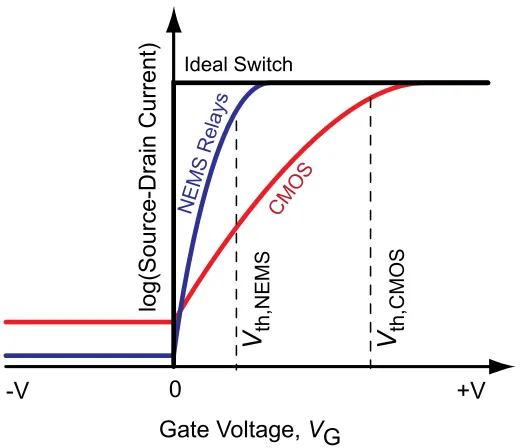
Figure 1.2: Voltage-current (I-V) plot comparing ohmic NEMS switch, CMOS, and ideal switch performance. The gate voltage, VG, is used to turn the device on resulting in current flow from source to drain. The higher sub-threshold slope of NEMS switch technology allows for the use of lower control voltages that reduce device power consumption per switching event.
The power consumption of a digital switch is characterized by power dissipated during both
the device off-state (VG<0) and on-state (VG>0). The former is the static power draw of the device and is known as sub-threshold leakage, while the latter is the dynamic switching power termed
the sub-threshold swing voltage. NEMS logic switches afford potential power savings in both of
these regimes [36], [37].
Sub-threshold leakage in CMOS is dominated by source-drain and gate leakage that scales
unfavorably with decreasing device dimensions [30]. This is seen as a current offset for voltages
below the turn on threshold voltage, Vt,CMOS, in figure 1.2. This leakage is due shorter and thinner oxide gate channels necessary to continue Moore’s Law scaling. Sub-threshold leakage in CMOS
currently represents ~50% of the total microprocessor power density [30] with standby leakage
currents of 1 nA/transistor having been reported at 250 nm gate-width node. This leakage is
dominated by gate leakage through the thin gate oxide [6] and continues to increase with device
downscaling. NEMS logic relays have already demonstrated leakage values five orders lower
Gate Voltage,
V
G
0
V
th,NEMSV
th,CMOSIdeal Switch
log(Source-Drain
Current)
NE MS
Re lays
CM
OS
7
than MOSFET at the single device level [38]. These lower leakage values owe to the presence of
a physical gap between the source and drain of NEMS relays that eliminates source to drain
leakage so long as the gap is > 2 nm [4]. Unique to mechanical relays, physical gaps between
gate structures and less leaky gate materials (in the case of piezoelectrically-actuated devices)
reduce gate leakage to near zero.
NEMS relays offer far lower dynamic switching power than CMOS. The sub-threshold swing
of a logic device describes the inverse slope of the I-V curve and represents the voltage
necessary to attain a decade change in current from source to drain [39]. Lower sub-threshold
swings correspond to lower turn-on voltages that confer lower active transistor power
consumption. The sub-threshold swing of CMOS is fundamentally, thermodynamically limited by
its operating mechanisms of electron drift and diffusion to 60 mV/dec [28] with current CMOS
demonstrating sub-threshold swings of 70 – 100 mV/dec [30], [39]. This translates to CMOS turn
on voltages of 0.3 – 1 V [40], which is several orders of magnitude larger than the minimum
voltage (a few mV) necessary for communication. NEMS prototype logic relays offer the lowest
sub-threshold slope of potential transistor replacement devices [30] with sub-threshold slopes of
0.03 – 2 mV/dec having already been demonstrated [19], [38], [41], and which translate to a
threshold voltage of just a few mV [19].
In addition to their lower power consumption, NEMS logic relays are amenable to application
spaces not accessible by CMOS. The functionality of CMOS relies critically on delicate doping
levels that require a low thermal budget and minimization of heat generation due to device
leakage is of current critical concern. Because NEMS logic does not rely on delicate doping
levels, these devices may be amenable to high temperature computing, which would allow for
smart sensors in previously inaccessible, harsh environments such as temperatures up to 500 ˚C
[2], [42], [43]. Furthermore, co-integration of NEMS relays with CMOS – which is possible due to
the low thermal budget of typical NEMS processing [4] – has lead to the exploration of
programmable gate array logic based on NEMS relays and traditional MOSFET [44], [45]. The
shocks [2], [42] , which makes these transistors attractive in military applications where
radiation-hard attributes are desired. Adhesion between the electrical contacts of NEMS relays may also
be used for nonvolatile memory applications where the switch retains its last state (open or stuck
closed) [46], [47]. NEMS relays are also amenable to three dimensional integration, which could
increase functional density per given real-estate of a microchip to continue Moore’s Law scaling
[47], [48].
1.3 The Nanoscale Electrical Contact is the Achilles Heel of NEMS Logic Switches
Despite the potential benefits of NEMS logic switches, tribological failure mechanisms at
the electrical contact interface currently limit commercial viability of the technology [4]. Transistor
functionality is critically dependent on maintaining high isolation in the off-state (switch open) and
low resistance in the on-state (switch closed). Failure due to stiction that results in permanent
welding of the switch interface, wear of contact materials, adsorbed layers of insulating
contaminant films on free surfaces, and insulating tribopolymer (TP)1 formation of
mechanochemical origin have been observed in microscale and nanoscale electrical contacts
testing [31], [50].
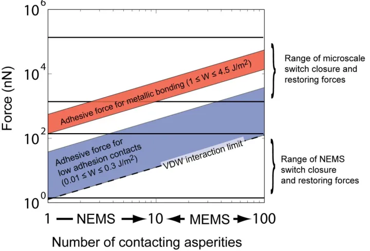
The effects of stiction, insulating contaminant layers, and TP formation are expected to
increase as NEMS relays are scaled down in size. This is a consequence of the dominance of
surface forces and the limited closure and separation forces available to NEMS relays. Figure 1.3
compares the closure and separation forces of micro- and nanoscale electrical switches and the
necessary separation force for single (the fundamental unit of contact in nanoscale switches) to
multiple contacting asperities indicative of multiasperity, microscale contacts. This approximation
shows that the surface forces of NEMS relay contacts will outpace the relative generative force of
the device. Microscale switches with soft, low hardness metallic electrical contacts (e.g. Au) have
9
been particularly susceptible to stiction due to electromigration or softening that results in contact
area growth [51]. Consequently, highly adhesive materials must be avoided to prevent stiction.
Figure 1.3: Separation force of electrical contacts of various work of adhesion ranges, W, as a function of the number of simultaneously interacting surface asperities. The adhesive interaction of the asperity is treated with DMT contact mechanics (eq. 2.8). Microscale MEMS contacts involve several to hundreds of contacting asperities while the ultimate limit of a NEMS contact is the single asperity. The adhesive force of nanoscale electrical contacts exceeds the restoring force of the actuator for small devices. NEMS logic switch contact materials favor low adhesion in order to limit stiction.
Inhibiting the formation of insulating TPs is expected to be the greatest challenge facing
nanoscale electrical contacts and is considered to be a function of the surrounding environment,
mechanical, electrical, and chemical properties of the electrical contact materials, and the
electrical power through the contacts. Figure 1.4 shows the effect of repetitive making and
breaking of microscale, multiasperity noble metal contacts under both cold cycling (voltage and
non-reactive materials, increases in contact resistance after 105 to 108 cycles can be seen and are attributed to the formation of short-chain carbon and oxygen contaminants [50]. The origin of
this effect appears to be mechanochemical in nature – the presence of free surfaces,
environmental contaminants, and pressure activate bond formation and chain lengthening. Even
hermetically-sealed devices have demonstrated similar behavior [49]. Recent evidence suggests
that operation of contacts in reducing environments such as oxygen can significantly reduce TP
buildup [52]. However, such device packaging can be costly to implement and limit the operation
space of the device. Ultimately, conductive and non-reactive electrical contact materials must be
sought.
Figure 1.4: Contact resistance as a function of make/break cycles for microscale noble metal electrical contacts of Au and Pt from various sources [50], [51], [53]. The formation of insulating TP results in a dramatic increase in contact resistance after a critical number of cycles. The use of highly adhesive contact materials can also lead to stiction of the switch.
1.4 Scaling Down: The Operational Requirements of NEMS Logic Switches with Comparison to MEMS Switches
The emphasis of this thesis is the study of nanoscale electrical contacts with application to
low power NEMS relay logic. However, NEMS relay topologies and most recent work on electrical
11
conditions at the electrical switch contact vary between the two technologies – especially in terms
of expected failure mechanisms and scaling considerations – when discussing the need for the
new contact test method described here.
MEMS relays have been implemented for power savings and superior functionality in radio
frequency systems [54], are now considered a mature technology [4], and several have been
commercially deployed. Many of the lessons learned for the contact behavior of conventional
switch materials (i.e. metals), like that shown in figure 1.4, can be attributed to work focused on
microscale, multiasperity MEMS contacts. The fundamental unit of contact, the single asperity,
which is the ultimate limit of NEMS contact can also be viewed as a single element of a
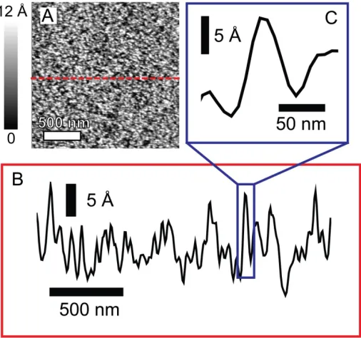
multiasperity contact (see figure 1.5). Error! Reference source not found. lists the salient differences between the contact environment and lifetime needs of NEMS and MEMS relays.
this thesis focuses on single asperity surface interactions that represent the fundamental unit of contact of a rough surface or the ultimate limit of contact size for NEMS logic switches.
Table 1.1: Comparison of the operational requirements of MEMS RF switches vs. NEMS logic switches.
MEMS RF Switches NEMS Logic Switches
Required lifetime
(cycles) 108 – 1011 [54], [55] 1015 - 1016 [4] Contact area of
conductive contacts
(m2) 10
-8 - 10-12 10-17 - 10-18
Adhesion Not explicitly treated Primary concern (impacts energy consumption and reliability) [4]
Device
contact/restoring force μN – mN [54] 5 – 150 nN
Voltage across the
contact 2 – 70 V Several mV to V
Current through the
device conact 50 – 150 mA [54] nA - μA
Current density at the
contact (A/m2) 109 – 1014 105 - 1011
Power (mW) <500 [54] <1
Maximum contact
resistance (Ω) 0.5 – 2 [54] <106
Dominant contact materials selection
characteristics
High conductivity and non-fouling
Moderate conductivity, non-fouling, and low adhesion
The lifetime requirements for NEMS logic switches differs substantially from RF MEMS
switches. Ohmic RF MEMS switches are designed as interrupts for radio frequency transmission
lines. While the contacts of these devices carry RF signals up to GHz frequencies, making and
breaking of the contact happens far less frequently, usually on the order of kHz or less, requiring
13
– thus, NEMS relays that are competitive with CMOS must exhibit nanosecond closure times,
which requires upwards of 1016 operating cycles without failure [4].
The electrical constraints and power handling requirements of the electrical contacts of
NEMS switches also differ substantially those of ohmic RF MEMS. Commercially viable ohmic RF
MEMS switches demand contact resistances from 0.5 - 2 Ω [54, p. 5] in order to minimize
insertion loses, which limits possible set of contact materials to high conductivity metals.
Permissible NEMS logic relay contact resistances have a broader range – from several kΩ up to
100 kΩ, depending on device topology and the electrical time constants of the implementation –
such that alternative, novel, and previously unconsidered materials (e.g. conductive oxides [56]
and conductive diamond-like materials [24]) could be implemented at the contact. Furthermore,
the power across ohmic RF MEMS contacts often reaches 100+ mW with power being
transferred across the contact after closure (cold switching). NEMS logic relays are expected to
experience, at most, a few mW of power across the contact and operate in a hot-switched mode
(bias applied across the contact during closure) with <1 V across the contacts during switching.
These differing switch contact environments ultimately affect the local conditions at the contacting
asperities that could change the degradation mechanisms of the contact. For instance, the high
voltages (10 V and higher) across the contacts of MEMS devices can lead to field evaporation
[57] that may not be a significant degradation mechanism in nanoscale NEMS switch contacts.
1.5 Existing Methods to Test Electrical Contact Reliability at the Microscale and the Need for a New Nanoscale Electrical Contact Test Method
Testing of electrical contacts for micro- and nanoscale electrical switches has been
typically achieved via two routes. New contact materials may be integrated directly into switch
designs or electrical contact materials are isolated and tested using mechanical testing
apparatuses that mimic the making and breaking of a switch. The former is generally
potentially superior, contact materials are avoided in lieu of materials that have proven ease of
fabrication. The use of mechanical test apparatuses are preferred for isolating the contact
material. However, as will be discussed in the following, previous microscale electrical contacts
suffers present several shortcomings that the work in this thesis addresses.
Evaluation of electrical contact materials at the microscale and outside of the device has
been achieved using modified scanning probe microscopy setups and nanoindentation. However,
these methods are time consuming and do not yield the number of interaction cycles expected for
NEMS switch electrical contact materials. Chen et al. [58] utilized a custom fabricated cantilever
that was brought into contact with various counter surfaces to investigate contact resistance
changes to noble metal contacts of ~5 μm radius for up to 107 contact cycles. While they were able to show significant increases in contact resistance (due to TP formation) for contacts of Ir,
Ru, and Au, the method the employ is limited to 800 cycles/sec., which means that only ~70
million contact cycles would take 1 day of testing. Similarly, Yang et al.[57] investigated Au/Au
microcontacts using a flexible cantilever terminating in microscale, multasperity contact in contact
with a flat counter surface to reveal significant material transfer under hot switching conditions.
This test was performed with 1 ms switching times, which translates to ~86 million cycles in a 24
hour period. Nanoindentation methods are even more limited in cycling throughput. Dickrell and
Dugger [59] utilized a modified nanoindenter of radius 1.6 mm in contact with a flat counter
surface to investigate Au/Pt contacts for up to 100 cycles. Measurements in their work spanned
several seconds per contact event significantly limiting the total number of cycles that could be
achieved.
While existing work on electrical contacts has revealed the role of contact materials and
switching environment on the longevitity of electrical contacts, it suffers from several issues that
limit applicability to nanoscale electrical contacts. Throughput is low, allowing only hundreds to
hundreds of millions of cycles per day of testing. Contacts are multiasperity with surfaces