ABSTRACT
MICK, STEPHEN EDWARD. Analysis and Design Considerations for AC Coupled
Interconnection Systems. (under the direction of Paul D. Franzon)
As the process technologies for microelectronic integrated circuits continue to improve,
both the amount of integrated, on-chip functionality and the number of required off-chip
interconnections (I/O) will continue to increase. These I/O will not only become more
numerous but also will need to be packed densely and be capable of operating both with
high bandwidth and low power. Packaging technology research is aimed at increasing I/O
density and circuit research is underway to improve the bandwidth and power performance
of I/Os. Advances are being made in each of these areas, but industrial roadmaps predict
that these advances will not keep pace with the needed improvements. The research in this
dissertation addresses this widening technological gap.
The central thesis in this work hinges on the recognition that arrays of densely packed,
low-power, high-bandwidth I/Os can be created if the physical structure of each I/O is
optimized for the type of information it must transmit. For example, the DC component of
digital signals carries no information. Instead, digital signals contain information at
frequencies well above DC (where the exact frequency spectrum of the information
depends upon the edge rate of the data transitions). This can be exploited by recognizing
that AC information can be transmitted across a boundary with non-contacting structures
only where DC signal transfers are needed. In this way, AC signal paths are freed from the
mechanical constraints of direct, contacting structures and both the compliance and rework
problems encountered in other high density interconnect technologies can be alleviated.
Capacitive and Inductive AC Coupled Interconnections are extensively analyzed and
measured in this work and presented as a means to provide an array of sub-100
µ
m pitched,
low-power, multi-gigabit per second per pin interconnections. A packaging structure that
ANALYSIS AND DESIGN CONSIDERATIONS FOR AC COUPLED
INTERCONNECTION SYSTEMS
by
STEPHEN EDWARD MICK
A dissertation submitted to the Graduate Faculty of
North Carolina State University
in partial fulfillment of the
requirements for the Degree of
Doctor of Philosophy
ELECTRICAL ENGINEERING
Raleigh
2004
APPROVED BY:
DEDICATION
BIOGRAPHY
Stephen Mick son of Dennis and Deborah Mick was born in August 1972 in Pasadena, Texas. In June of
1995, Stephen married Julie Miller and in December of that same year earned his B.S. in Electrical
Engineering from the University of Houston. While completing his undergraduate degree, Stephen worked for
three semesters at Texas Instruments as part of the cooperative education program. After graduation he
continued working at Texas Instruments until he and his wife moved to North Carolina to continue their
respective educations. Stephen earned his M.S. in Electrical Engineering from North Carolina State University
in December 1998 and then investigated several possible Ph.D. research topics and interned for LSI Logic in
ACKNOWLEDGEMENTS
Foremost I would like to thank God the Father for His grace, constant provision, answered prayer and
redemption through the death and resurrection of the Lord Jesus Christ. Not only is faith in Christ eternally
significant but also it has shaped my life and helped me to keep perspective when graduate school seemed
overwhelming.
I would like to thank my advisor, Dr. Paul Franzon for giving me the opportunity to work in his research
group. Paul has made available every resource I could possibly need and has allowed me the independence to
pursue topics often tangential to the research in this dissertation. In spite of his very busy schedule Paul has
always had time to answer questions and provide guidance when needed. I also want to thank Dr. John Muth,
Dr. Rhett Davis and Dr Jacqueline Krim, the members of my advisory committee, for their comments,
suggestions and support.
The packaging aspect of this work has been done in collaboration with MCNC and I would like to thank those
both formerly or presently associated with this project. Specifically, Alan Huffman and Sundeep Nangalia
(who has since moved to another company) were very helpful in the early stages of the project when we were
trying to determine whether the concept of recessed solder bumping would even work. I also want to thank
Sal Bonafede who has been an enormous help both technically and logistically in developing the MCNC
substrate process.
The staff of the cleanroom here at NC State deserves much credit. Joan, Harold, Ginger, Henry, and Myrick
run a great facility and have always been willing to offer assistance, training on the tools and lab space for my
experiments.
I would also like to thank Lei Luo and the other members of the project whose rapid progress in their own
topics has inspired me to finish and whose insights into the technical problems (and potential solutions) of AC
Coupled Interconnects have been helpful in formulating the approach I took in my research. I also want to
thank Steve Lipa, Dr. John Wilson, and Jayesh Nath for their countless hours of help with acquiring and
analyzing measurements. Not only has John helped immensely with measurements but also he has been an
excellent sounding board for technical questions on this project and has been relentless in pushing me to “just
get finished”.
John Damiano and David Nackashi have been excellent friends throughout this entire process. I want to thank
I also want to thank Michele Joyner who has always been helpful in ordering supplies, making travel plans,
tracking down paychecks and reimbursements, and navigating the trail of paperwork that must coincide the
entire graduate school process.
I want to thank all of our family for their love and support. It was tough for Julie and I to leave everyone and
come to North Carolina for school but our family has always been there for us, cheering us on every step of
the way.
Finally, I want to thank the love of my life – my wife Julie. We have been down a long, hard road together
Table of Contents
List of Tables ...x
List of Figures...xi
Chapter 1 Introduction...1
1.1 Problem Statement ...1
1.2 Motivation and Objectives...2
1.3 Dissertation Overview ...2
1.4 Original Contributions...2
1.4.1 AC Coupling...2
1.4.2 Coupling Elements ...3
1.4.3 Packaging...3
1.5 Publications...3
1.5.1 Journals...3
1.5.2 Conferences...3
1.5.3 Presentations...4
1.5.4 Patent ...5
Chapter 2 Literature Review ...6
2.1 Overview ...6
2.2 AC Coupled Interconnection...6
2.2.1 Capacitive Coupling ...6
2.2.2 Inductive Coupling...8
2.3 Integrated Passive Elements ...9
2.3.1 Inductor Modeling ...9
2.3.2 Transformer Modeling...12
2.3.3 Inductor Performance in CMOS Technologies...13
2.3.4 Inductor Performance in non-CMOS Technologies ...14
2.3.4.1 Post-processing...14
2.3.4.2 Multichip Modules ...15
2.4 Packaging Technology...15
2.4.1 Background ...15
2.4.2 Packaging Trends ...17
2.4.3 Substrate Technologies ...19
2.4.4 Physical Packages ...22
2.4.5 Bonding Processes ...23
2.4.5.1 Solder Joining ...23
2.4.5.2 Sea of Polymer Pillars (SoPP) ...23
2.4.5.3 Conductive Materials...24
2.4.5.4 3D Bonding ...24
2.4.5.5 Hybrid Bonding...24
3.2.1 Lumped CCI System...27
3.2.2 Distributed CCI System ...31
3.2.2.1 Capacitively-Coupled Network Terminated by Low Impedance...31
3.2.2.2 Effect of Lossy Transmission Line on Distributed CCI System ...35
3.2.2.3 Performance of Complete Distributed CCI System ...36
3.3 Inductively Coupled Interconnects...36
3.3.1 Coupled Inductor Model...36
3.3.2 Correlation of Model to Physical Geometry ...39
3.3.3 Model Development and Analysis ...43
3.3.3.1 Inductance...43
3.3.3.2 Coupling Coefficient ...46
3.3.3.3 Winding Resistance...51
3.3.3.4 Parasitic Capacitance...56
3.3.4 Discussion ...66
3.3.4.1 Lumped LCI System ...70
3.3.4.2 Distributed LCI System Performance...70
3.3.4.3 Coupled Inductor Density...74
3.4 LCI versus CCI ...74
Chapter 4 CCI and LCI Measurements ...78
4.1 Overview ...78
4.2 Capacitive Coupling ...78
4.2.1 Experimental Design...78
4.2.2 Measured Results ...80
4.3 Inductive Coupling ...82
4.3.1 Experimental Design...83
4.3.1.1 Inductor Geometric Variations...83
4.3.1.2 Transformer Geometric Variations ...88
4.3.1.3 Alignment and Crosstalk...91
4.3.2 Measured Results ...94
4.3.2.1 Inductor Geometric Variations...95
4.3.2.2 Transformer Geometric Variations ...99
4.3.2.3 Alignment and Crosstalk...109
Chapter 5 Package Development...113
5.1 Overview ...113
5.2 Packaging for AC Coupling...113
5.3 Fabrication Process Tradeoffs...115
5.3.1 Gap Height Uniformity and Trench Design...116
5.3.2 Coupling Element Density ...116
5.3.3 Chip-Substrate Alignment...117
5.3.4 Transmission Lines ...117
5.4 NCSU Process...118
5.5.1 Modeling ...123
5.5.2 Process Flow...127
5.5.3 Experimental Design...128
5.5.4 Transmission Line Results ...129
5.5.5 Process Limits and Density ...133
Chapter 6 Future work...137
6.1 Coupling Elements...137
6.2 Transceiver Design ...137
6.3 Substrate Fabrication...137
6.4 CAD Tools...138
List of Tables
Table 1 Device classifications in ITRS Roadmap [83]...18
Table 2 Inductors designed to study electrical impact of geometric variations in the TSMC 0.35µm process 84 Table 3 Model values for asymmetric inductor designs generated by OEA Spiral ...86
Table 4 Model values for symmetric inductor designs generated by OEA Spiral...86
Table 5 Effective inductance for symmetric inductors driven as single-ended elements ...87
Table 6 Model values for inductor designs generated by ASITIC at 1GHz ...88
Table 7 Geometric parameters of transformers designed for the TSMC 0.35µm process ...89
Table 8 Geometric parameters of transformers designed for the TSMC 0.25µm process ...89
Table 9 Model values for TSMC 0.35µm transformer designs predicted by ASITIC ...91
Table 10 Model values for TSMC 0.25µm transformer designs predicted by ASITIC ...91
Table 11 Primary and secondary inductor geometries to study effect of lateral offset upon inductor coupling 92 Table 12 Lateral offsets for transformer alignment experiments ...92
Table 13 Model values for TSMC 0.35µm transformer alignment experiments A1-A4 predicted by ASITIC 93 Table 14 Model values for TSMC 0.35µm transformer alignment experiments C3-C10 predicted by ASITIC ...94
Table 15 Model values for TSMC 0.35µm inductor crosstalk experiments predicted by ASITIC...94
Table 16 Measured and extracted values for TSMC 0.35µm inductors...96
Table 17 Comparison of extracted values for TSMC 0.35µm inductors and values predicted by Spiral and ASITIC ...97
Table 18 Extracted values for TSMC 0.35µm transformers...100
Table 19 Extracted values for TSMC 0.25µm transformers...105
Table 20 NCSU cleanroom substrate process flow ...118
Table 21 DC Resistance of isolated microstrip transmission lines on metal levels 3 & 4...129
List of Figures
Figure 1: Illustration of AC Coupled Interconnection using series, trans-chip capacitive coupling elements ....7
Figure 2: Illustration of AC Coupled Interconnection using shunt, trans-chip inductive coupling elements ...9
Figure 3: Common 9-element lumped inductor model...10
Figure 4: Lumped model for inductor with one grounded terminal ...11
Figure 5: Narrowband model of inductors generated by ASITIC ...12
Figure 6: Narrowband model of transformer generated by ASITIC ...13
Figure 7: Packaging I/O Requirements 2001-2016 [82]...17
Figure 8: Triplate lines for IBM Thin-Film Module technology [89]...20
Figure 9 Circuit schematics for lumped and distributed CCI systems ...26
Figure 10 Geometrical parameters for coupling capacitor design...26
Figure 11 Frequency-domain responses demonstrating impact of RLupon lumped CCI channel...28
Figure 12 Time- and frequency-domain responses of lumped CCI channel to varying ratios of CC / CP with 1MΩload ...29
Figure 13 Ratio of CP/ CCas a function of 1) the ratio of distance between capacitor plates and substrate, and 2) the ratio of relative permittivities of inter-capacitor dielectrics and substrate ...30
Figure 14 Magnitude and phase responses of lumped CCI channel...32
Figure 15 Time-domain response of a lumped CCI channel to input voltage steps with varying rise time ...33
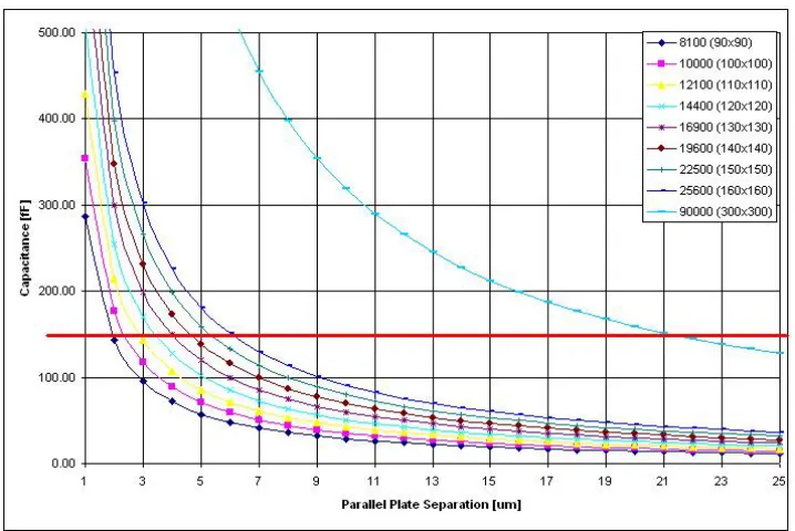
Figure 16 Capacitance between opposing plates versus plate area and separation...35
Figure 17 Lumped element model of coupled inductors ...37
Figure 18 Lumped element model of single-ended coupled inductors ...37
Figure 19 Simplified coupled inductor model (basis of analysis) ...38
Figure 20 Schematic of a lumped LCI system ...39
Figure 21 Schematic of a distributed LCI system...39
Figure 22 Geometrical parameters for coupled inductor design (isolated) ...40
Figure 23 Coupling coefficient as a function of z-offset ...41
Figure 25 Equivalent models of perfectly coupled inductors ...43
Figure 26 Magnitude and phase responses of four sets of ideal coupled inductor...45
Figure 27 Step response for ideal coupled inductors ...46
Figure 28 Equivalent models of coupled inductors with imperfect coupling ...47
Figure 29 Magnitude and phase response of coupled inductors with varying coupling coefficient ...48
Figure 30 Magnitude and phase response of coupled inductors for different values of load impedance...49
Figure 31 Step response of coupled inductors with varying coupling coefficient and low impedance termination ...50
Figure 32 Step response of coupled inductors with varying coupling coefficient and high impedance termination ...50
Figure 33 Equivalent models of coupled inductors with imperfect coupling and winding resistance ...51
Figure 34 Impact of winding resistance upon magnitude response of perfectly coupled inductor for 50Ω termination ...52
Figure 35 Impact of winding resistance upon magnitude response of imperfectly coupled inductor for 50Ω termination ...53
Figure 36 Impact of winding resistance upon magnitude response of imperfectly coupled inductor for 500Ω termination ...54
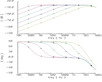
Figure 37 Impact of winding resistance upon step response for system terminated in 50Ω...55
Figure 38 Impact of winding resistance upon step response for system terminated in 500Ω...56
Figure 39 Equivalent model of coupled inductors with imperfect coupling, winding resistance, and parasitic capacitance ...57
Figure 40 Magnitude response of coupled inductors with parasitic capacitance ...58
Figure 41 Equivalent models of coupled inductors with imperfect coupling, parasitic capacitance and winding sense ...59
Figure 42 Trajectories of poles and zeros of coupled inductors with same phase and opposite phase windings as a function of coupling capacitance CC...61
Figure 43 Time domain response of coupled inductors with coupling capacitance (CC) ...62
Figure 47 Impact upon frequency response due to variations in resistive substrate loss (RP)...67
Figure 48 Ladder network replacement of RWfrom coupled inductor model to capture skin effect resistance 68 Figure 49 Comparison of LCI models with increasing levels of detail...69
Figure 50 Transformer impedance (magnitude and phase) seen by load due to variations in resistive substrate loss (RP) ...71
Figure 51 Schematic of distributed LCI system with complete coupled inductor models ...72
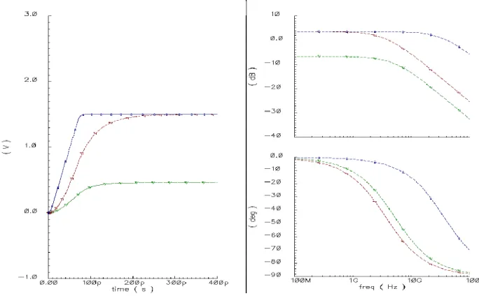
Figure 52 Voltage waveforms and eye diagrams of distributed LCI system transmitting 5Gbps NRZ data...73
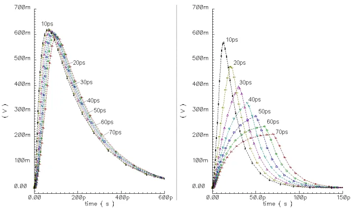
Figure 53 Time-domain performance of LCI versus CCI with air dielectric between plates...75
Figure 54 Time-domain performance of LCI versus CCI with non-air dielectric (εr≈4) between plates...76
Figure 55 Die photo of capactively-coupled driver and receiver experiments in the TSMC 0.35µm process ..79
Figure 56 Schematic of receiver for capacitive coupling experiments...79
Figure 57 Performance of capacitively-coupled driver and receiver connected through an off-chip bondwire with 2GHz input square wave ...81
Figure 58 Performance of capacitively-coupled driver and receiver connected through an off-chip bondwire with 3GHz input square wave ...82
Figure 59 Photographs of inductor and transformer experiments fabricated in TSMC 0.35µm and TSMC 0.25µm processes...83
Figure 60 Photographs of two inductor experiments fabricated in the TSMC 0.35µm process...85
Figure 61 Lumped, asymmetric inductor model generated by OEA Spiral...85
Figure 62 Lumped, symmetric inductor model generated by OEA Spiral...86
Figure 63 Lumped, narrow band inductor model generated by ASITIC ...87
Figure 64 Photographs of two transformer experiments fabricated in the TSMC 0.35µm process ...89
Figure 65 Photographs of two transformer experiments fabricated in the TSMC 0.25µm process ...90
Figure 66 Lumped transformer model generated by ASITIC ...90
Figure 67 Photographs of transformer experiments derived from design C3 with increasing lateral offset and fabricated in the TSMC 0.35µm process...93
Figure 68 Model of inductor used to match measured data...95
Figure 71 Time- and frequency-domain performance of extracted and predicted models for inductor B3 and B6 ...98
Figure 72 Model of transformer used for matching measured data...99
Figure 73 Measured (de-embedded) and extracted S11and S22magnitude / phase response of transformer C3
...100
Figure 74 Measured (de-embedded) and extracted S12and S21magnitude / phase response of transformer C3
...101
Figure 75 Time- and frequency-domain performance of extracted and predicted models for transformers A1 and C3 ...102
Figure 76 Measured (de-embedded) and extracted S11, S22, S21, S12 magnitude and phase response of
transformer L50w...103
Figure 77 Time- and frequency-domain performance of extracted and predicted models for transformers L50wb and L75wb ...104
Figure 78 Extracted coupling coefficient versus ratio of vertical offset to transformer diameter for transformers fabricated in the TSMC 0.35µm and TSMC 0.25µm processes ...106
Figure 79 Comparison of measured S21for TSMC 0.25µm transformers ...107
Figure 80 Measured eye diagrams for transformer experiments A1 and C1-C3 fabricated in the TSMC 0.35µm process subject to a 3.5Gbps NRZ, PRBS input signal...108
Figure 81 Measured eye diagrams for transformer experiments A1 and C1-C3 fabricated in the TSMC 0.35µm process subject to a 1.0Gbps NRZ, PRBS input signal...109
Figure 82 Measured eye diagrams for transformer alignment experiments A1 – A4 fabricated in the TSMC 0.35µm process subject to a 3.5Gbps NRZ, PRBS input signal...110
Figure 83 Measured eye diagrams for transformer alignment experiments C3 – C10 fabricated in the TSMC 0.35µm process subject to a 3.5Gbps NRZ, PRBS input signal...110
Figure 84 Measured eye diagrams for transformer crosstalk experiments D6 – D10 fabricated in the TSMC 0.35µm process subject to a 3.5Gbps NRZ, PRBS input signal...111
Figure 85 Measured peak voltage as a function of lateral offset for TSMC 0.35µm transformer alignment experiments C3 – C10...112
Figure 86: Top-down and side-view cross-sections of physical structure to support both buried solder bumps and AC coupled interconnections...114
Figure 87 Circuit-level view of packaging structure...115
Figure 91 Top-down photograph of substrate after joining and separation demonstrating 100% solder bump yield ...122
Figure 92 NCSU substrate test structure showing yield loss of metal routing layer over edge of trench feature ...122
Figure 93 Critical parameters for design of embedded transmission lines...124
Figure 94 Possible configurations for transmission lines with a 50Ωcharacteristic impedance...125
Figure 95 HFSS simulation results of dielectric thickness versus conductor width for 50Ω buried microstrip lines ...126
Figure 96 HFSS simulation results of attenuation for embedded microstrip lines versus dielectric and geometry...127
Figure 97 Cross-section of layer stackup for MCNC substrate process...128
Figure 98 Plot of DC resistance measurements of isolated microstrip transmission lines on metal levels 3 & 4 ...130
Figure 99 TDR measurements of MCNC wafer #15, metal 3 transmission lines...131
Figure 100 Metal 3 transmission line characteristic impedance versus line width ...132
Figure 101 Inductance values achievable with MCNC substrate process as a function of inductor diameter and the number of metal levels containing spiral windings...134
Figure 102 3-D perspectives of 4-turn, 100µm diameter single- and two-layer inductors with metal width and spacing equal to 5µm ...135
Figure 103 Layout snapshot of fully routed 32 x 32 array of differential AC connections and 16x32 array of DC connections in MCNC process ...135
Chapter 1 Introduction
1.1
Problem Statement
The demand is increasing rapidly for high density, high bandwidth off-chip I/O. Though the average densities
implied by the ITRS roadmap are not too different from solder bump densities achievable today, the peak I/O
densities in future products are expected to present a technological barrier to existing interconnection
methodologies [1].
Many researchers are addressing the need for increased I/O density by trying to find methods to manufacture
cost-effective, reliable solder bump interconnections with a pitch of 100µm or less. However, there are many
known difficulties with achieving such pitches [2, 3, 4]. The compliance issues faced by small solder bumps are
well known, and many attempts have been made to produce high aspect ratio solder bumps with some success
but little impact due to manufacturing cost issues. A new process presented here uses buried solder bumps in
conjunction with AC coupled interconnects to solve the problems introduced by continually shrinking the size
and pitch of solder connections with current solder bump technologies.
In addition to increasing I/O density, a number of circuit design researchers are trying to develop methods to
increase the bandwidth of each I/O by building new circuit topologies capable of multi-Gbps signaling.
Approaches being explored include source-synchronous techniques to limit the effects of clock skew [5];
small-swing differential techniques to improve toggle rate and power-per-bit [6]; and equalization to compensate for
the skin effect [6].
The structure presented in this dissertation recognizes that the goals of high density and high bandwidth can be
achieved simultaneously by optimizing the interconnection structure for each type of signal that needs to be
carried off-chip. That is, DC signals can be communicated by direct, mechanical connections and AC signals can
be communicated off-chip by AC coupled connections. However, new transceiver circuits must be developed to
exploit the properties of AC Coupled interconnections and a physical structure must be developed that provides
an interface between chip and substrate compatible with the requirements of both DC and AC connections.
The structure developed in this dissertation will presently allow for 2533 I/O in a 310mm2chip area where 844
of the I/O are direct mechanical connections for DC signals and each of the remaining I/Os provide a fully
differential, non-contacting AC signal path. This density exceeds the needs stated by the ITRS industry roadmap
1.2
Motivation and Objectives
The research presented in this dissertation has been guided by several system-level goals. For example, it is a
goal to develop a system that supports a high-density of interconnections (meeting the ITRS packaging roadmap)
and that can communicate data at high bandwidths (≥3 Gbps) with low power (~40 mW per I/O). To this end,
coupling elements suitable for implementation in both CCI and LCI system have been developed and
characterized. A substrate fabrication process to support AC Coupled systems has been designed and
transmission lines in this process have been characterized. Although development continues on this substrate
process, the work in this dissertation will provide future researchers with design guidelines and experimental
results necessary to develop a complete system.
1.3
Dissertation Overview
The ultimate goal of investigating AC Coupled systems is the development of high-speed, low-power,
chip-to-chip communication systems with dense arrays of I/Os. The concepts of AC signal coupling, integrated coupling
elements, and packaging are fundamental to the work presented in this dissertation and Chapter 2 reviews
previous work in each of these areas.
Analysis of both capacitive and inductive ACCI systems is presented in Chapter 3 and measurements are
presented in Chapter 4. System integration issues such as packaging, routing and coupling element density are
presented in Chapter 5. The dissertation is concluded with suggestions for future work in Chapter 6.
1.4
Original Contributions
The original contributions of this research are subdivided into categories relating to specific aspects of this
research.
1.4.1 AC Coupling
• Demonstration of 6Gbps NRZ data transmission through a series of two capacitively-coupled stages through an off-chip connection
• Analysis of coupled inductor model culminating in simulations showing feasibility of 5Gbs uncompensated signaling through inductively coupled channels.
1.4.2 Coupling Elements
• Development and validation through measurements of a model for coupled inductors
1.4.3 Packaging
• Design and prototype of buried solder bump package
• Co-development of a substrate fabrication process and transmission lines to support AC Coupled interconnections
1.5
Publications
To date, Mr. Mick’s work has been published in a peer-reviewed journal, conference proceedings, and has been
presented numerous times. A patent application has been filed on the work presented in this dissertation related
to integrating AC Coupling with a new package structure.
1.5.1 Journals
Mick, S., Luo, L., Wilson, J., and Franzon, P., "Buried Bump and AC Coupled Interconnection Technology",
IEEE Transactions on Advanced Packaging, 27(1), Feb 2004.
1.5.2 Conferences
Franzon, P., Kingon, A., Mick, S., Wilson, J., Luo, L., Chandrasekar, K., Bonafede, S., Statler, C., LaBennett,
R., “High Frequency, High Density Interconnect Using AC Coupling”, MRS 2003 Symposium B: Materials,
Integrations, and Packaging Issues for High-Frequency Devices, Invited Paper, B6.1, Materials Research
Society, Boston, Dec 1-5, 2003.
Franzon, P., Mick, S., Wilson, J., Luo, L., Chandrasekar, K., “AC Coupled Interconnect for Density
High-Bandwidth Packaging”, 2003 International Conference on Solid State Devices and Materials, Tokyo, Japan,
Sept. 16-19, 2003.
Mick, S., Wilson, J., Luo, L., Chandrasekar, K., Franzon, P., “AC Coupled Interconnect for Dense 3-D
Mick, S.; Franzon, P.; “Design Guidelines for Inductive AC Coupled Interconnects”, SRC Techcon 2003,
Semiconductor Research Corporation, Dallas, Texas, Aug 2003
Mick, S.; Luo, L.; Wilson, J.; Franzon, P.; “Buried Solder Bump Connections for High-Density Capacitive
Coupling”, Proceedings of the IEEE Electrical Performance of Electronic Packaging Conference, IEEE,
Monterey, California, Sept. 2002, pp 205-208.
Mick, S.; Franzon, P.; Huffman, A. “Packaging Technology for AC Coupled Interconnection”, Flip-Chip
Technology Workshop 2002, Proceedings of the International Microelectronics And Packaging Society, IMAPS,
Austin, Texas, June 2002.
Mick, S.; Wilson, J.; Franzon, P.; “4 Gbps high-density AC coupled interconnection”, Proceedings of the IEEE
2002 Custom Integrated Circuits Conference, Invited Paper, IEEE, Orlando, Florida, May 2002, pp 133-140.
Excerpts reprinted as Mick, S., Wilson, J., and Franzon, P., "AC scheme bumps I/O density," EE Times, 1218,
CMP / United Business Media, May 13, 2002, pp 67,72.
Mick, S.; Franzon, P.; “AC Coupled Interconnect”, SRC Techcon 2001, Semiconductor Research Corporation,
Dallas, Texas, Sept. 2001.
1.5.3 Presentations
This research has been presented on numerous occasions to industry partners and to funding agencies. Following
is a list of presentations Mr. Mick has made:
“ACI for Space Electronics: Inductively-Coupled Circuit Issues”, US Air Force Program Review, September
2003, Raleigh
“AC Coupled Interconnect”, Tasks 1094.001 and 1094.002, SRC ICSS Program Review, September 2003,
Seattle
“Design Considerations for Inductive AC Coupled Interconnect”, SRC Techcon, August 2003, Dallas
“AC Coupled Interconnect”, Task 722.001, SRC Back-end Packaging Program Review March 2003, Tucson
“AC Coupled Interconnect”, Task 722.001, SRC Back-end Packaging Program Review March 2002,
1.5.4 Patent
Buried Solder Bumps for AC-Coupled Microelectronic Interconnects; SRC Patent ID: P0237; Inventors:
Chapter 2 Literature Review
2.1
Overview
The demand is increasing rapidly for high density, high bandwidth off-chip I/O. Though the average I/O
densities implied by the ITRS roadmap are not too different from solder bump densities achievable today, the
peak I/O densities in future products are expected to present a technological barrier to existing interconnection
methodologies [1]. AC Coupled interconnects can provide a solution to this technological barrier. A complete
AC Coupled system is composed of a transceiver, capacitive or inductive coupling elements and
interconnections. Opposing metal plates on two ICs or on an IC and a substrate being brought into close and
controlled proximity can create the capacitive coupling elements needed to implement an AC Coupled system.
Similarly, opposing inductors on two ICs or on an IC and a substrate being brought into close and controlled
proximity can form inductive coupling elements. The transceiver must be designed to compensate for the
frequency response of the coupling elements and interconnections.
The ultimate goal of investigating AC Coupled interconnects is to support the development of a high-speed,
low-power, chip-to-chip communication system with dense arrays of I/Os. Given the function and composition of
such a system, the concepts of AC coupling of signals, integrated coupling elements (both capacitors and
coupled inductors) and packaging are fundamental to the work presented in this thesis. A rich body of literature
exists in each of these areas, and no single body of literature pulls together the information necessary to employ
coupling elements and interconnections in the creation of a high-density, high bandwidth chip-chip
communication system. Instead, innovations in each area must be reviewed to reveal the issues to be considered
when designing an AC Coupled communication system.
2.2
AC Coupled Interconnection
The basic concept of AC coupling exploits the fact that capacitors placed in series or coupled inductors placed in
parallel with an AC signal trace can block any DC voltage while passing the AC voltage. Both capacitive and
inductive signal coupling can be used to transmit signals containing AC information across an interface where no
direct physical connection exists. AC Coupling can be exploited in both on-chip and off-chip applications.
Moreover, it can be used to transmit information across a chip-chip or chip-substrate boundary.
2.2.1 Capacitive Coupling
to provide frequency compensation to op-amps [8]. Consecutive stages of multi-stage analog circuits exploit
series coupling capacitors to keep the DC biases from the various stages isolated [9].
Gabara explored a quantized feedback receiver topology that used an integrated on-chip coupling capacitor with
one side of the capacitor connected directly to an I/O pin and the other side connected to the input of the receiver
[10]. Gabara’s technique re-established a local DC level at the receiver thereby enabling non-encoded data to be
recovered across a wide frequency range (2000Hz – 800MHz) [10].
Capacitive coupling does not have to be confined to capacitors that are completely on-chip. Instead, capacitive
coupling can take advantage of the fact that two metal plates will form a capacitor when brought into close
proximity of each other. Metal plates can be fabricated on either side of a physical interface and when the two
surfaces are brought close enough to each other and the metal plates aligned, a capacitor is formed. AC coupling
can be realized if this capacitor is connected as a series circuit element as illustrated in Figure 1. Capacitive
coupling can be exploited in this way to transmit electrical signals from a rotating shaft to a stationary receiver
[11]. It can also be used for IC boundary scan testing [12]; as a position sensor [13]; to directly couple signals in
3D packaging [14]; and to communicate information between multiple ICs [15, 16].
Figure 1: Illustration of AC Coupled Interconnection using series, trans-chip capacitive coupling elements
Knight proposed using capacitive coupling across a physical interface as a means to transmit signals between
multiple ICs on a common MCM substrate [15]. In this implementation, Knight claimed that signals could be
demonstrated chip-chip capacitive coupling at data rates of 4Gbps NRZ [18]. Kanda continued with this idea and
proposed an implementation of capacitive coupling in the context of 3D IC packaging [19].
Kuijk et al. reported using capacitive coupling to connect the output of a silicon, CMOS ring oscillator to a diode
rectifier fabricated on a III-V substrate [16]. The researchers aligned metal plates on the top surfaces of each of
the silicon and III-V substrates and brought the ICs into close proximity of each other. They suspended the two
ICs from each other by creating a gap filled with a high permittivity, liquid dielectric to increase the coupling
capacitance. The resulting structure was then sealed to prevent the dielectric from leaking out from between the
two ICs.
Implementations of capacitive coupling across an interface are not restricted to point-to-point connections.
Chang has proposed using capacitive coupling as a means to transmit multiple CDMA data signals between ICs
along a single, common substrate transmission medium [20].
2.2.2 Inductive Coupling
Inductive coupling is often treated as a parasitic effect for on-chip wiring [21, 22, 23]. However, intentional
(rather than parasitic) inductive coupling has found use in many applications. On-chip coupled inductors (i.e.
transformers) find use in distributed power amplifiers [24], LNAs [25, 26], and mixers [27].
Wong et al. recognized that the capacitance between two on-chip, vertically-aligned, coupled inductors cannot be
ignored. These researchers used the phrase “capacitively coupled transformer” to describe the on-chip capacitor
/ transformer hybrid that they designed and characterized for use in an LNA [26].
Like capacitive coupling, inductive coupling does not have to be confined to coupling elements that are
completely on- or off-chip. Inductive coupling can take advantage of the fact that two inductors will form a
transformer when brought into close proximity of each other. Individual inductors can be fabricated on either
side of a physical interface and when the two surfaces are brought close enough to each other and the coupling
elements aligned, a transformer is created. AC coupling can be realized if this transformer is connected as a
circuit element as illustrated in Figure 2.
AC coupling between ICs with inductive elements has found many applications. For example, Chuah et al.
reported a strain measurement system designed to be embedded in concrete that transferred both power and a
signal across an inductively coupled-interface. [28]. Glaser reported work to transfer power and all I/O signals
with inductive coupling and thereby eliminate the need for any physical interconnections [29]. In Glaser’s work
Inductive coupling between ICs has also been used in smart card applications to provide a non-contacting
interface between smart cards and their receivers [30, 31]. The on-chip inductors used for this type of application
are often large requiring an area of approximately 3mm2[30].
Figure 2: Illustration of AC Coupled Interconnection using shunt, trans-chip inductive coupling elements
Recently, Mizoguchi reported on the development of a transceiver in which inductive coupling is used to
communicate information between two ICs stacked directly on top of each other [32]. The inductors used in this
study are 300µm per side and the communication distance through the ICs is 300µm although only simulated
waveforms are presented.
2.3
Integrated Passive Elements
AC Coupled systems implemented with inductive coupling rely upon integrated passive inductors and the
performance of transformers built from these inductors. Numerous researchers have developed models of
integrated inductors to aid in the design process and many performance results have been reported for on-chip
inductors and transformers integrated into CMOS-based devices and substrates.
2.3.1 Inductor Modeling
inductors on silicon is shown in Figure 3 [34, 35, 36, 37]. This model is used to create a frequency-independent
representation of an inductor’s electrical behavior.
The key to modeling is in understanding of the major mechanisms that must be modeled [37]. With reference to
the model in Figure 3, the parameters of this model correspond to physical quantities [34, 37, 38]:
• LS– series inductance
• RS– winding resistance
• CS– series feed-forward capacitance between the two inductor terminals
• COX– capacitance between inductor and substrate due to inter-level dielectric
• RSI– resistance of substrate
• CSI– capacitance across substrate
Figure 3: Common 9-element lumped inductor model
Variations of the model can be found in [34, 35, 36, 37]
Although it is not perfect, this model provides good correlation with measured results by capturing the behavior
of crossover capacitance, substrate capacitance, substrate loss, and oxide capacitance [38]. The skin effect
(which causes RSto increase with increasing frequency) is not modeled directly. However, shortcomings with
this model are not a surprise since the model simplifies a complex distributed system into nine lumped elements.
Many variations exist on the basic inductor model presented in Figure 3. For example, Niknejad has used four
different variations of this model [39, 40, 41]. Crols used a model similar to this for inductors on a lowly doped
silicon substrate but did not include CSIand CS[42]. Yue noted that if one terminal of the inductor were to be
Figure 4: Lumped model for inductor with one grounded terminal
Yue reported a five-step method to extract the parameter values for a lumped inductor model from measured data
[38]:
1. Measure S-Parameters of inductor
2. De-embed effects of measurement testbed
3. Convert S-Parameters to ABCD-Parameters
4. Solve for propagation constant and characteristic impedance from ABCD parameters
5. Solve for model values from propagation constant and characteristic impedance.
Ashby reported that de-embedding the measurement testbed could be accomplished by subtracting the
Y-Parameters of the testbed from the Y-Y-Parameters of the inductor [34]. However, Niknejad warned that parasitic
coupling between the testbed and inductor complicates de-embedding the effects of the testbed from the inductor
[41]. This coupling is present during inductor measurements but is not present during testbed-only
measurements unless the testbed and the inductors are carefully isolated. Groves cautioned that the inductors
should be measured across the desired operating temperature range since the Q of inductors over conductive
silicon (15Ω-cm, P-type) decreases with increasing temperature [43].
Although it can be instructive to fit measured data to a model; it is also useful to develop a model that can be
used to predict performance. Mohan et al developed analytic expressions to predict the values of the 9-element
model parameters (from Figure 3) for square, hexagonal, octagonal, and circular inductor geometries [36]. With
these formulas, inductors and circuits containing inductors could be designed and optimized without having to
Niknejad developed a CAD tool named ASITIC (Analysis and Simulation of Inductors and Transformers for
ICs) that enables design, optimization, and modeling of spiral inductors and transformers [41]. ASITIC is freely
available (http://rfic.eecs.berkeley.edu/ ~niknejad/asitic.html) and models every segment of an inductor or transformer with a lumped model and uses electromagnetic techniques to compute inductance and capacitance
matrices. This tool can be used to create lumped, narrowband models of inductors (Figure 5) using the built-in
‘pix’ command.
Figure 5: Narrowband model of inductors generated by ASITIC
Koutsoyannopoulos and Papananos developed a CAD tool named SISP (Spiral Inductor Simulation Program) to
“accurately model polygonal (i.e. square, octagonal) spiral inductors, both planar and 3-D, transformers, and
center-tapped spirals, splitters, and baluns” [45]. This CAD tool models every segment of a structure with a
2-port lumped model that is capacitively, inductively, and resistively coupled to all other segments. Its creators
validated the performance of this tool by comparing simulated performance with the measured performance of
inductors fabricated by several commercial foundries. This tool is now sold commercially
(http://www.elab.ntua.gr/sisp/) but does not model stacked, coupled inductors.
2.3.2 Transformer Modeling
Mohan presented a number of topologies by which integrated transformers can be modeled and manufactured
including tapered, interleaved and stacked [46]. Other researchers have also presented models and design
equations for planar, coupled inductors [41, 45, 47, 48, 49, 50]. Of the topologies possible for coupled inductors,
only stacked transformers are relevant to AC coupled interconnection systems. Mohan presented a lumped
model of a stacked transformer where both primary and secondary are on the same integrated circuit. In his
model, Mohan had an explicit connection between inductors with shared capacitance to ground. Mohan also
Verma developed an ABCD-Parameter model from Mohan’s lumped-element transformer model [51].Verma
derived expressions for the 2-port S-parameters of a stacked transformer from his ABCD network model. Verma
also developed a method to extract model parameters from measured S-parameter data by decomposing
parameter extraction into two sub-problems: low-frequency and high-frequency parameter extraction.
ASITIC can be used to create lumped, narrowband models of transformers with the topology shown in Figure 6
using the built-in ‘calctrans’ command [52]. As shown in Figure 6, the ASITIC ‘calctrans’ command creates
models for transformers that do not include the parasitic capacitances intrinsic to coupled inductors.
Figure 6: Narrowband model of transformer generated by ASITIC
Zolfaghari proposed a multi-metal topology for an integrated stacked transformer in which the primary coil was
fabricated in a mid-level metal (of a multi-level metal process) and the secondary was fabricated on the
remaining metal levels (both above and below the primary) [53]. Zolfaghari also proposed a subtle technique to
improve transformer performance whereby the windings between stacked transformers were offset. This
technique did not affect the mutual coupling between the primary and secondary but it reduced the parasitic
capacitive coupling.
2.3.3 Inductor Performance in CMOS Technologies
Researchers have identified design techniques to overcome some of the inherent performance limitations with
integrated inductors and transformers. For example, Niknejad advocated octagonal inductors instead of square
Park investigated the effect of substrate resistivity and inductor geometry upon the inductor quality factor and
found that Q increases with increasing substrate resistivity [55]. Park validated his findings by fabricating and
measuring inductors with substrate resistivities of 4-6Ω-cm, 30-50Ω-cm, and 2 kΩ-cm. A process that relies
upon highly resistive substrates is not widely transferable to commercial foundries since CMOS substrate
resistivity is usually kept low to avoid latch-up.
Yue proposed the use of a patterned ground shield between the substrate and an inductor to reduce substrate
coupling while improving the inductor quality factor [56]. Yue claimed that by using a patterned ground shield to
eliminate substrate coupling, the design of on-chip inductors would be “simplified to a trade-off between the
series resistance (RS) and the oxide capacitance (COX)” [37].
Long found that inductor Q is limited by the thin interconnect metallization available from commercial
foundries; so he advocated thicker metal interconnections as a means to improve Q [57]. Long measured a
1.8nH inductor fabricated in a BiCMOS process and found that at 3GHz, increasing the conductor thickness
from 1µm to 3µm can double the Q of the inductor from 5 to 10.
Burghartz proposed using inductors created from multiple metal levels and connected with via arrays to create
inductors with an increased effective conductor thickness [58]. Burghartz fabricated inductors to test his theory
in a process that supplied four AlCu metal levels where the top-level metal was 2µm thick and the lower-level
metals were each 1µm thick. The process also used a 1.5µm thick dielectric between each metal layer and a 3µm
thick dielectric between the substrate and the first metal layer. Burghartz found peak Q for inductors fabricated
from a combination of all of the top-three metal layers supporting the claim that thicker conductors lead to higher
Q.
Ashby proposed using an AT&T BiCMOS fabrication process with both highly resistive substrates and 5µm to
6µm gold metallization [34]. In this process, Ashby found that it was the DC resistance of the inductor spirals
that limited peak Q to 12 across a frequency range from 3GHz to 4GHz.
2.3.4 Inductor Performance in non-CMOS Technologies
2.3.4.1
Post-processing
Rogers developed a method to post-process CMOS inductors with copper electroplating to increase the
conductor thickness to 4µm [59]. Rogers was able to achieve a peak Q of 17 at 2GHz with a 250µm diameter
Ahn proposed the use of integrating magnetic core materials to create toroidal inductor structures through
post-processing techniques on CMOS and bipolar integrated circuits [60]. The inductors in this process are large (on
the mm scale) and achieve peak inductance in the low-MHz frequency range.
2.3.4.2
Multichip Modules
Inductor performance can be improved in a number of ways including increasing the resistivity of the substrate,
using thick conductors, and creating a large gap between the inductor and the substrate. While these
improvements prove taxing to CMOS integrated inductors, each improvement can be easily applied to inductors
integrated onto packaging substrates such as MCMs [61, 62].
Arnold and Pedder reported the performance of thin-film spiral inductors in an MCM-D technology [63]. These
researchers used silicon coated with silicon dioxide as a substrate and had a fabrication process that supplied four
metal levels with polyimide as an inter-level dielectric. The wiring rules in this technology supported 25µm wire
widths on 75µm pitch. Inductors with Q values ranging from 7 - 8 between 1GHz and 3GHz were demonstrated.
Allen reported methods to fabricate inductors in MCM-L technologies [64].
Other researchers have been able to increase the Q of inductors in silicon-based MCM-D technologies by
increasing substrate resistivity [65], increasing the thickness of the dielectric layers [66], and decreasing the
minimum line width and spacing of metal traces [67]. Much of the current MCM-D research has been focused
upon creating RF systems that rely upon integrated inductors rather than upon continued modeling of integrated
inductors [68, 69, 70]. Researchers have also investigated integrating inductors into MCM-L and MCM-C
substrates and making RF systems in these technologies [71, 72, 73, 74].
2.4
Packaging Technology
AC Coupled systems rely upon IC packaging technology to bring coupling elements into close proximity.
Packaging has a long history including research in areas such as substrate processes, physical packages, and
bonding methods. Each of these areas is relevant to AC Coupled Interconnection system design.
2.4.1 Background
Since the early days of integrated circuits, companies have been developing packaging technologies to build
multi-component systems. Texas Instruments delivered to the U.S. Air Force the first computer built from
complexity. In 1964, IBM developed a method used in its IBM/360 computers to bond glass-encapsulated
transistors, diodes and passive components into logic modules. This packaging technology was called SLT and
was touted as offering “integrated circuits having close to maximum performance” due to its reduction of
parasitic interactions between components, long lifetime without hermetically sealed devices, and manufacturing
yields [76]. IBM documented the use of SLT with the creation of an AOI logic module. Solder was used to
connect devices to the substrate. However in this technology, the solder from underneath the devices was free to
wet the metal interconnections on the substrate. Rigid copper balls were used to prevent the devices from
crashing into the substrate during solder reflow and causing short circuits between terminals.
In late 1968, IBM announced a method to bond flipped chips that did not rely upon rigid copper spheres or
solid-state metallurgical interactions [77]. Miller recognized that if the solder-wettable surfaces on the substrate were
controlled, then during reflow the surface tension of the solder could be used to suspend the devices above the
substrate until the solder re-solidified. This technique would thereby prevent collapse-induced electrical shorts.
Further, the use of “controlled collapse” allowed soft, ductile materials to be used for solder pads and eliminated
the need for rigid contacts.
The advantages of controlled collapse over SLT and other rigid contact methods were numerous. The soft,
ductile solder pads could withstand far more stress during thermal cycling and this led to reduced strain and
fewer contact failures [77]. Moreover, the controlled collapse technique allowed for more tolerance in the
planarity between bonding surfaces since solder could be deformed during reflow. The reduced need for
planarity between bonding surfaces allowed “multi-pad devices of significant size and complexity” [77].
Miller discussed in detail several methods to restrict the areas to which solder could move during reflow
including dots, dams, overlap, isolated lands and extra pads [77]. The dam method involved depositing a
non-tinnable barrier material on top of non-tinnable landing pads to define regions where solder could form a joint. This
new joining method proved to be very reliable. In pre-production studies, bond yields of 97% were observed
[77]. Further studies investigated the thermal stability of controlled-collapse solder joints [78,79], optimization
of landing pad geometry and solder volume [80], and optimization of solder composition [81].
Area array technologies have had a long and successful history of being employed in IC packages on advanced
devices. However, for years, the cost associated with area array packaging has kept this technology from being
applied in applications that were either too cost-sensitive or did not demand high I/O density. Instead, many
packages were developed that relied upon all circuit I/Os being made available on the perimeter of the IC.
2.4.2 Packaging Trends
Industry roadmaps make projections as to the number of signal, power and ground I/Os that future ICs will have
to support [82]. Figure 7 shows the ITRS projection for package I/Os from 2001 to 2016. This roadmap makes
projections for several classes of devices including low cost, cost-performance and high-performance devices
(see Table 1) [83].
0 1000 2000 3000 4000 5000 6000 7000 8000
2000 2002 2004 2006 2008 2010 2012 2014 2016 2018
Year
Pi
n
C
ount
low cost
cost-performance high-performance
Figure 7: Packaging I/O Requirements 2001-2016 [82]
It is projected that the pin count for high-performance ICs will increase to 7100 I/Os by the year 2016 for a die
size of 310mm2[82]. The roadmap indicates that technologies capable of supporting this high density have been
identified although they are not yet proven to be transferable to industrial manufacturing. Further, no solution is
known to exist that will achieve the required roadmap density while also meeting the roadmap cost-per-I/O
Table 1 Device classifications in ITRS Roadmap [83]
Device Class
Description
Low-Cost
<$300 consumer products, microcontrollers,
disk drives, displays
Hand-Held
<$1000
battery-powered
products,
mobile
products,
hand-held
cellular
telecommunications, other hand-held products
Cost-Performance
<$3000 notebooks, desktop personal computers,
telecommunications
High-Performance
>$3000
high-end
workstations,
servers,
avionics,
supercomputers,
most
demanding
requirements
Harsh
Automotive (under the hood) and other hostile
environments
Memory
DRAMs, SRAMs
One effect of the demand for increased I/O density is to drive I/O pitch to ever-smaller levels. Wirebonding
technology (fundamental for perimeter-style packages) has advanced to support the demanded I/O pitches using
innovations such as multiple rows of bonding pads and ultra thin bonding wires. However, this technology is
beginning to reach its limit since the I/O pitch continues to shrink [84,85]. Present day wirebonding systems can
create rows of ultra-high pitched wirebonds on a pitch of 45 - 60µm [86,87]. Commercial wirebonding system
manufacturers however have admitted that flip chip area array packaging will eventually be more cost effective
for applications requiring high density since numerous manufacturing and cost issues exist in creating reliable,
ultra high-pitch wirebond connections [84].
Another effect of the demand for higher I/O density is the development of smaller packages. There are currently
four major classes of packages: through-hole, surface mount, area array, and 3-D – although there are hybrid
through-hole / area array packages such as PGAs.
Through-hole packages are mounted to substrates by rigid leads that pass completely through the substrate. The
density that these packages can support is limited due to difficulties in miniaturizing the package pins and
through-substrate connection sites.
Surface mount packages are mounted to the surface of substrates by rigid leads that flare in or out at the bottom
of the package. Surface mount devices can be made to have very small footprints. In this type of package ICs are
connected to the internal package pads by bondwires. Thus, the pitch at which bondwires can be reliably
The solution to the problem of high-density interconnections must be addressed at many levels. Work is being
done to improve interconnection density of substrate technology including array depopulation, microvias and
thin-film technologies. The two techniques of microvias and thin-film substrates are recognized as being
fundamental to enabling future PCBs to support the demands for increased I/O density [88]. Work is also being
done to design substrates that will ensure signal integrity and manufacturing methods are being developed for
creating fine-pitched arrays of solder bumps. Some researchers, however, propose schemes that represent a
paradigm shift over present interconnection technology.
2.4.3 Substrate Technologies
A designer must consider the pin density that a particular substrate technology can support when designing an IC
for area array, flip-chip packaging. In perimeter bonding technologies, the wirebond pitch translates directly into
the substrate wiring pitch. However, for flip-chip applications, an array of coarsely spaced connections can
require wiring rules more stringent than those required for fine-pitched perimeter-only connections. For example,
consider the wiring rules for both a perimeter and an area array package with I/O on 60µm pitch. With perimeter
packaging, all I/O could be routed if the wiring rules could support 30µm wide lines on a 60µm pitch. For the
area array, however, the wiring rules would have to support 10µm wide lines on a 10µm pitch just to route two
rows of the array with a single layer.
Wiring with 10µm wide lines would result in unacceptable resistive losses. For example, a 50Ω stripline
fabricated from copper with a 5µm×9µm cross-section would have a resistance per unit length of 4Ω/cm [89].
Rather than shrinking wire pitch and width to achieve all wiring on a single layer, more layers can be added to
the substrate, but adding routing layers increases cost and manufacturing complexity.
For cost efficiency, some manufacturers develop infrastructure for a single base array bump size and pitch that is
compatible with their existing low-cost substrates [90]. The area array bump size and pitch is designed to
accommodate the most stringent I/O requirements that the manufacturer will support. Designs requiring fewer
I/Os use the same bump sizes as the base array but allow for a larger bump pitch by not populating every site on
the base array. This technique of depopulation has the effect of easing the substrate wiring rules for designs that
do not require the highest I/O density [90]. For companies that employ depopulation, it is important that the base
array bump size and pitch be carefully chosen since all other designs must use it.
Researchers are investigating techniques to create miniaturized vias (i.e. microvias) to mitigate the large via
core. The researchers measured the effects of CTE mismatch between the organic materials and the FR-4, the
thermal resistance of the organic materials, and the moisture sensitivity of the organic materials. The researchers
concluded that their manufacturing technique could produce microvias down to 50µm on a 225µm pitch and was
suitable for use with flip chip bonding. However, they admitted that manufacturing microvias smaller than
50µm in diameter would require more research due to problems with plating such small vias.
Depopulation and microvias do not deal with the pressing need to develop substrates that support ultra dense
wiring. Accordingly, much ongoing research is aimed at developing substrate processes that can support finely
pitched, narrow width conductors. Realistic wiring rules must be developed by balancing electrical performance
with cost and fabrication complexity, and many issues must be considered when defining electrical performance
including crosstalk, switching noise, insertion loss, dispersion and delay.
Ho et al reported a detailed study of the electrical performance tradeoffs for IBM’s Thin-Film Module process
[89]. This process consisted of two metal ground layers sandwiching two wiring layers and a topmost metal
layer for fan-out. Copper was the preferred metal and polyimide (withεr≈3.5) was the preferred dielectric. To
ensure acceptable electrical performance, constraints existed upon the fabrication process. It was noted that RIE
must be used to etch both vias and wiring templates for electroplating. The process must also support metal lines
and vias with large aspect ratios (metal height÷metal width). Finally, each layer must be fabricated with 10%
planarity in order to control transmission line impedance.
With such a fabrication process, Ho et al found that thin-film lossy lines could be used to propagate high-speed
pulses with low distortion over distances up to 20cm [89]. The researchers investigated crosstalk performance for
thin-film lossy lines. They developed the structure shown in Figure 8 (with dimensions inµm) that maintained a
50Ωimpedance, could support 1000 lines per inch over 20cm line lengths, and suffered less than 10% crosstalk.
The transmission lines shown in Figure 8 were characterized byρCu= 1.8µΩ-cm, Ro= 4.1Ω/cm, Lmax= 2Zo/Ro
(at 20cm), and Zo= (L22/C22)1/2= 41Ω. Ho and his colleagues also reported a method to integrate capacitors into
Haller and his colleagues reported electrical results of microstrip and stripline transmission lines fabricated with
a GE high-density interconnect thin-film process [92]. The process employed four metal layers and three
dielectric layers. From the bottom of the substrate to the top, the dielectrics were 50µm, 21µm, and ~15µm
thick. All conductor layers were made of copper and were approximately 4µm thick.
In this fabrication process, TDR measurements confirmed that microstrip lines of 78µm on a 138µm pitch and
striplines of 51µm, on a 111µm pitch maintained a 50Ωcharacteristic impedance [92]. VNA measurements were
made of insertion and return losses. The researchers found a good correlation between theoretical and measured
losses once the process details were taken into account. That is, once the conductors were fabricated, they had a
trapezoidal rather than a rectangular cross-section. The researchers defined the “effective height” of the
trapezoidal conductors such that the perimeter was identical to the idealized rectangular conductors assumed by
their microstrip and stripline equations. The need to define an effective height is important since the effective
geometry of thin film structures cannot be known until the details of the fabrication process have been
determined. Thus, the wiring rules cannot be set until the tolerances of the fabrication process are known (or at
least specified) [89, 92, 93, 94].
Another important finding was that for the given transmission line dimensions, insertion loss rather than
crosstalk noise dominated interconnect performance for frequencies up to 9GHz [92]. The process must be
modified to create lines that are not as lossy or transmitter and receiver circuits capable of communicating across
lossy lines must be designed.
Substrates can be manufactured in more than one way but performance consistency across manufacturing
methods is important. Thiel, et al. reported an effort to study the effects on high frequency signal transmission in
thin film MCM-L substrates. The substrates that they studied adhered to the Motorola MRTV-2.2 / Interconnect
Technology Research Institute specification ITRI-TV2.4A specification [95]. This substrate specification was
developed to be compatible with current techniques for substrate fabrication. As an example, the substrate vias
could be manufactured with photolithography, laser ablation, mechanical punching, or plasma etching. Although
their data analysis was targeted toward MCM-L substrates and it was incomplete, they discussed several
important aspects of substrate manufacturing that could impact performance consistency across different
manufacturing techniques. The researchers noted that the electrical performance of interconnections on thin film
substrates was a function of the substrate surface roughness, substrate dielectric thickness, dielectric constant,
conductor cross-section, parasitics, and fabrication process tolerances. These findings underscore the fact that
found, for several reasons, that FR-4 is not a suitable substrate material for high-speed signal propagation [96].
The loss tangent of FR-4 is 0.025 and this leads to unacceptable signal loss over long connections (e.g. 10.8dB
loss over 70cm at 2GHz). Materials with lower loss tangents are needed to support high-speed signal
propagation.
Signal propagation delay for transmission lines on any particular material is a function of the dielectric constant
of the material, and FR-4 has a relative dielectric constant of approximately 4.3. Power dissipation is also a
function of a material’s dielectric constant. Substrate materials with lower dielectric constants are being sought
to reduce both signal propagation delay and power dissipation [96]. Moreover, cost, fabrication constraints, and
moisture absorption (since moisture affects the stability of the dielectric constant) must all be considered when
selecting a new substrate material [97].
Given the large number of variables that must be optimized, the absolute limits of substrate wiring are unclear.
Pease and his colleagues make the argument that at room temperature, coplanar substrate interconnections on a
line pitch of 35µm are feasible. The pitch can be shrunk to 6µm if the substrate is cooled to liquid nitrogen
temperatures and to 2µm if superconducting interconnections are used [98].
Alternatives to the traditional use of substrate interconnections are being explored as methods to support an
effective increase in I/O density. For example, if the frequency of data communication is high enough, the
substrate traces interconnecting I/Os between ICs must be treated as transmission lines. In this situation, the
transceiver circuits and interconnection can be specifically designed so that multiple bits of data can be in-flight
simultaneously on the transmission line [99]. Per I/O data rates of up to 1Gbps have been achieved with this
method.
2.4.4 Physical Packages
In addition to the substrates, much attention has been focused on the physical packaging for solder bump, area
array technologies. Numerous packages based on these technologies and variations thereof are reported as
evidenced by the articles on BGA [100, 101, 102, 103, 104], flip chip [101, 105, 106, 107], CSP & WLP [101,
108, 109, 110], and MCM [111, 112, 113, 114].
Organizations such as JEDEC help define standards for packages [115]. These standards set ranges for package
features and are useful in maintaining consistency between packages implemented by different manufacturers.
For example, JEDEC standard MO211-B defines the size, location and height tolerances for CSP packages
Newly developed packages must be qualified by lifetime tests to ensure reliability in harsh environments [118].
For example, thermal cycling tests expose the major failure mechanism in BGA packages – solder joint cracking
and delamination due to fatigue from thermal cycling [119]. It has been found that BGA reliability is
dramatically improved by the use of underfill materials since these materials distribute across the entire package
surface the stress induced by solder and package CTE mismatches [119].
There is an indistinct boundary between substrates and packaging for MCMs since MCMs act as both a substrate
to interconnect multiple ICs and packaging to a PCB for these ICs. Like substrates, fabrication processes for
MCMs must be carefully developed to ensure acceptable electrical performance for interconnections and
manufacturing yield [120, 121,122, 123].
2.4.5 Bonding Processes
2.4.5.1
Solder Joining
The need for higher I/O densities drives continuing research in solder bump processes. Companies are involved
in providing services for flip chip packaging and are working on many different techniques to create bumping
processes capable of extremely high density. Current high-volume, production equipment for BGA packages is
able to place 300µm diameter solder balls but machines with 200µm capability are in field trials [124]. Texas
Instruments reports a WLP bump transfer process used to attach 127µm eutectic Sn / Pb solder bumps to an IC
on a 356µm pitch although there are plans to study smaller pitches [125]. Motorola has developed a process to
apply eutectic Sn / Pb solder to an IC by stencil printing and can achieve a 200µm solder bump pitch [126].
Using fine-line photolithography and solder electroplating, Unitive reports the ability to create 20µm solder
bumps on a 50µm pitch [127]. However, the composition of the Unitive
![Figure 7: Packaging I/O Requirements 2001-2016 [82]](https://thumb-us.123doks.com/thumbv2/123dok_us/1217904.1153111/34.612.150.481.195.449/figure-packaging-i-o-requirements.webp)
![Figure 8: Triplate lines for IBM Thin-Film Module technology [89]](https://thumb-us.123doks.com/thumbv2/123dok_us/1217904.1153111/37.612.217.413.547.648/figure-triplate-lines-ibm-film-module-technology.webp)