Design of Nested Neutral Point Clamped (Nnpc) Inverter with
Induction Motor for Capacitor Voltage-Balancing Method
Boorugupalli Vishnu Vardhan & Dr. K. Shashidhar Reddy
1M.Tech (Student), St.Martin’s Engineering College Affiliated To Jntuh, Hyderabad, Telangana, India. 2professor, St.Martin’s Engineering College Affiliated To Jntuh, Hyderabad, Telangana, India
ABSTRACT- In this paper proposes a capacitor voltage-balancing method for a nested neutral point clamped (NNPC) inverter with induction motor. The NNPC inverter is a newly developed four-level voltagesource inverter for medium-voltage applications. The Induction motor is a three phase AC motor and is the most widely used machine. A capacitor voltage-balancing method for a nested neutral point clamped (NNPC) inverter is proposed in this paper. To control and balance flying capacitor voltages the proposed capacitor voltage-balancing method takes advantage of redundancy in phase switching states. In this project we are implementing the induction motor because it has the characteristic features such as Simple and rugged construction and Low cost and minimum maintenance. The proposed method needs very few computations and also easy to implement. The NNPC inverter is a newly developed four-level voltage source inverter for medium-voltage applications. The proposed method is easy to integrate with different pulse width modulation schemes. By using the simulation results we can analyze the effectiveness and feasibility of the proposed method. Index Terms—Capacitor voltage-balancing method, multilevel inverter, nested neutral point clamped (NNPC) inverter, Induction motor, voltage source inverter
INTRODUCTION
Nowadays, Multilevel inverters are very popular in medium voltage applications and motor drives due to reduction of harmonics, low voltage stress on switches, low switching frequency, and less switching losses [1]. The multilevel inverters categorized into neutral point clamped (NPC) inverter, flying capacitor (FC) inverter, cascaded H-bridge inverter, and modular multilevel converter [2]–[3].
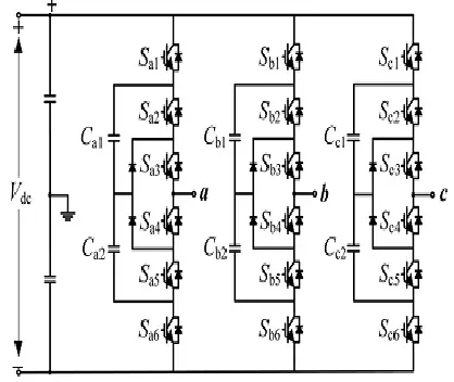
Several control techniques and modulation strategies including capacitor voltage-balancing methods have been developed in the literature for multilevel inverters [4]. In this paper a new multilevel topology is proposed. i.e, nested neutral point clamped (NNPC) inverter shown in Fig. 1.
This topology is a combination of an FC topology with an NPC topology, which provides four levels in output voltage. In comparison with the four-level NPC inverter, the NNPC inverter has less number of diodes, and in comparison to four-level FC inverter, it has fewer capacitors [6]. All switches in the topology have the same voltage stress equal to one-third of dc-link voltage. The NNPC inverter can
operate in a wide range of 2.4– 7.2 kV without the need for connecting power devices in series.
Fig. 1. Three phase nested neutral-point clamped
(NNPC) inverter.
As can be seen from Fig. 1, the NNPC topology has two FCs in each leg. The voltage across each capacitor should be controlled and balanced at one-third of dc-link voltage (Vdc/3) to ensure that the inverter can operate normally [6].
In order to mitigate the aforementioned drawbacks, a new capacitor voltage-balancing method for the NNPC inverter is proposed in this paper. In the proposed method, simple logic tables are developed to control the voltages of FCs. The proposed method has the following features:
1) The method is suitable for and can be easily integrated with different pulse width modulation (PWM) schemes such as SPWM and SVM, etc;
2) The method uses simple logic tables, needs very few computations, and is easy to implement. The difference in the topology causes different behavior in capacitor voltages and thus need different voltage-balancing methods.
OPERATION OF THE NNPC INVERTER AND BEHAVIOR ANALYSIS OF THE CAPACITOR
VOLTAGES A. Operation of the NNPC Inverter
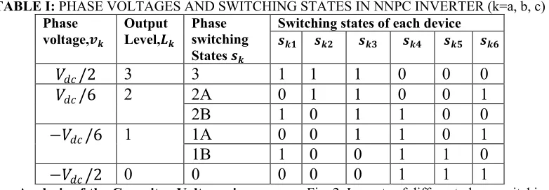
The three-phase NNPC inverter is shown in Fig. 1. Each phase of the inverter consists of six switches, two clamping diodes, and two FCs. The voltages of the FCs should be kept at one-third of dc bus voltage (Vdc/3) to generate four output levels in phase voltage and ensure that all the power switches share the same voltage stress. Table I shows the phase voltagevk (k=a, b, c), output levelLk, as well as the corresponding phase switching stateSk.
For each phase, the four distinct output voltages are −Vdc/2, −Vdc/6, Vdc/6, and Vdc/2,
corresponding to the four output levels 0, 1, 2, and 3, respectively. The relationship of vk and Lk can be expressed as
𝑣𝑘= 2𝐿𝑘− 3 𝑉𝑑𝑐/6 (1)
As can be seen from Table I, levels 0 and 3 have no redundant switching state, while levels 1 and 2 both have two redundant switching states. The redundant switching states for level 1 are 1A[001101] and 1B[100110]. The two redundant switching states generate the same output voltage−Vdc/6with different switches ON and OFF. For level 2, the two redundant switching states are 2A[011001]and 2B[101100], generating the same phase voltage Vdc/6 with different switches ON and OFF.
TABLE I: PHASE VOLTAGES AND SWITCHING STATES IN NNPC INVERTER (k=a, b, c)
Phase voltage,𝒗𝒌
Output Level,𝑳𝒌
Phase switching States 𝒔𝒌
Switching states of each device
𝒔𝒌𝟏 𝒔𝒌𝟐 𝒔𝒌𝟑 𝒔𝒌𝟒 𝒔𝒌𝟓 𝒔𝒌𝟔
𝑉
𝑑𝑐/2
3
3
1
1
1
0
0
0
𝑉
𝑑𝑐/6
2
2A
0
1
1
0
0
1
2B
1
0
1
1
0
0
−𝑉
𝑑𝑐/6
1
1A
0
0
1
1
0
1
1B
1
0
0
1
1
0
−𝑉
𝑑𝑐/2
0
0
0
0
0
1
1
1
B. Behavior Analysis of the Capacitor Voltages in the NNPC Inverter
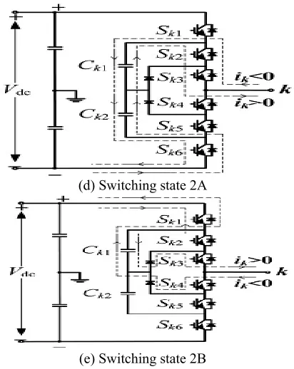
Different redundant switching states have different impacts on FC voltages. The analysis of this impact is illustrated in Fig. 2, in which the six overall switching states are analyzed.
In Fig. 2, Ck1 andCk2 are the two series FCs in the phase k(k=a, b, c), whose voltages are denoted byVCk1 andVCk2. The behavior of the capacitor voltages depends on the switching state Sk and the phase current ik.
(a) Switching state 0.
Fig. 2. Impacts of different phase switching states and phase current on capacitor voltages in NNPC
inverter
As shown in Fig. 2(a) and (f), the switching states 0 and 3 (corresponding to levels 0 and 3, respectively) have no impact on the capacitor voltages due to the fact that no current flows through the capacitors.
(f) Switching state 3
Fig. 2. Impacts of different phase switching states and phase current on capacitor voltages in NNPC
Levels 1 and 2 always have impacts on capacitor voltages. The impacts are different for different redundant switching states and also depend on the direction of phase current.
(b) Switching state 1A
Fig. 2. Impacts of different phase switching states and phase current on capacitor voltages in NNPC
inverter
For level 1, if the redundant switching state 1A is employed and ik >0, the capacitorCk2discharges andVCk2 decreases, and if ik <0, the capacitor Ck2 charges andVCk2 increases, while there is no impact on capacitorCk1,asshown in Fig. 2(b).
If the redundant switching state 1B is employed, both the capacitorCk1 andCk2 charge and capacitor voltage VCk1 andVCk2 increase when ik >0, and both Ck1 andCk2 discharge andVCk1 andVCk2 decrease when ik <0,as shown in Fig. 2(c).
(c) Switching state 1B
Fig. 2. Impacts of different phase switching states and phase current on capacitor voltages in NNPC
inverter
A similar analysis can be applied to level 2 as shown in Fig. 2(d) and (e) for the redundant switching states 2A and 2B.
(d) Switching state 2A
(e) Switching state 2B
Fig. 2. Impacts of different phase switching states and phase current on capacitor voltages in NNPC
inverter.
Table II summarizes the behaviors of FC voltages under different switching states and phase currents. As analyzed above, levels 0 and 3 have no impact onVCk1 andVCk2, while level 1 (with redundant switching state 1A and 1B) and level 2 (with redundant switching state 2A and 2B) have different impacts on VCk1 andVCk2 depending on the selected switching state and the direction of phase current.
PROPOSED CAPACITOR VOLTAGE-BALANCING METHOD A. Algorithm of the Proposed Method
If there is no control on the voltages of the FCs in the NNPC converter, the FC voltages will deviate from their desired value, and this is because there is no control over the currents that flow into/out from the capacitors. The difference between the actual FC voltage and the desired value (Vdc/3) can be defined as voltage deviation of the FC and can be expressed as
∆𝑉𝐶𝑘𝑖 = 𝑉𝐶𝑘𝑖 − 𝑉𝑑𝑐/3 (2)
Where VCki are the capacitor voltages and ΔVCki are the deviations of the capacitor voltages, k=a, b, c, and i=1,2.
TABLE II: BEHAVIOR OF FC VOLTAGES UNDER DIFFERENT PHASE SWITCHING
STATES AND PHASE CURRENTS
Phase voltage, Output Level, Phase Current
The behavior of flying capacitor voltages
𝑣𝑘 𝐿𝑘 𝑖𝑘 𝑉𝑐𝑘1 𝑉𝑐𝑘2
Vdc/2 3 - No change No change
Vdc/6 2 > 0 Decrease(2A)
Increase(2B)
Decrease(2A), Nochange(2B)
< 0 Increase(2A) Decrease(2B)
Increase(2A) Nochange(2B)
-Vdc/6 1 > 0 Nochange(1A)
Increase(1B)
Decrease(1A), Increase(1B)
< 0 Nochange(1A) decrease(1B)
Increase(1A) Decrease(1B)
-Vdc/2 0 - No change No change
Table III shows the logic table for controlling capacitor voltageVCk1. The following cases are listed in the table:
1) If ΔVCk1 <0, the switching state 2A should be selected if ik <0; otherwise, the switching state 2B is employed if ik <0;
2) If ΔVCk1 ≥;0, the switching state 2B should be selected if ik <0; otherwise, the switching state 2A is employed if ik≥;0.
In this condition, the capacitor voltage VCk1 is completely controllable regardless of the direction of the inverter phase current.
TABLE III: LOGIC TABLE FOR BALANCING
CAPACITOR VOLTAGE VCk1
Input conditions Output Results
𝐿𝑘 ∆𝑉𝑐𝑘1 𝑖𝑘 The selected switching
state 𝑠𝑘 for controlling
𝑉𝑐𝑘1
2 < 0 < 0 2A
≥ 0 2B
≥ 0 < 0 2B
≤ 0 2A
Table IV shows the logic table for controlling capacitor voltageVCk2. Similar to Table III, the following cases are listed:
1) If Δ; VCk2 <0, the switching state 1A should be selected if ik <0; otherwise, the switching state 1B is employed if ik ≥;0;
2) If Δ; VCk2 ≥;0, the switching state 1B should be selected if ik <0; otherwise, the switching state 1A is employed if ik ≥;0.
TABLE IV: LOGIC TABLE FOR BALANCING
CAPACITOR VOLTAGE VCk2
Input conditions Output Results
𝐿𝑘 ∆𝑉𝑐𝑘1 𝑖𝑘 The selected switching state 𝑠𝑘 for controlling
𝑉𝑐𝑘1
2 < 0 < 0 1A
≥ 0 1B
≥ 0 < 0 1B
≤ 0 1A
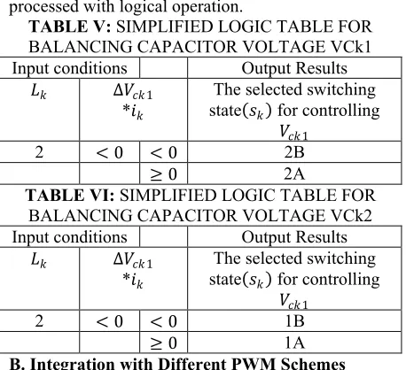
The simplified tables are given in Tables V and VI. In this case, ΔVCki×ik is used as input variable and the logic is simplified into two cases for each table. ΔVCki×ik could also be replaced by sign (ΔVCki)×sign(ik)and the operator “×” could be processed with logical operation.
TABLE V: SIMPLIFIED LOGIC TABLE FOR
BALANCING CAPACITOR VOLTAGE VCk1
Input conditions Output Results
𝐿𝑘 ∆𝑉𝑐𝑘1
*𝑖𝑘
The selected switching state 𝑠𝑘 for controlling
𝑉𝑐𝑘1
2 < 0 < 0 2B
≥ 0 2A
TABLE VI: SIMPLIFIED LOGIC TABLE FOR
BALANCING CAPACITOR VOLTAGE VCk2
Input conditions Output Results
𝐿𝑘 ∆𝑉𝑐𝑘1
*𝑖𝑘
The selected switching state 𝑠𝑘 for controlling
𝑉𝑐𝑘1
2 < 0 < 0 1B
≥ 0 1A
B. Integration with Different PWM Schemes The proposed capacitor voltage-balancing method is suitable for and can be easily integrated with different PWM schemes. The schematic diagram for integration is shown in Fig. 3, which could be summarized into the following four steps:
1) First, the output voltage level Lk can be generated by different PWM schemes, such as SPWM, SVM, etc.
2) The voltage deviationΔVCk1 andΔVCk2 should be calculated by (2), and also, the direction of the phase current ik should be determined;
3) Tables V and VI are employed to determine the best redundant switching state out of 1A, 1B and 2A, 2B;
Fig. 3. Schematic diagram for integration of the proposed capacitor voltage-balancing method with
PWM schemes.
This procedure indicates that the proposed capacitor voltage balancing method can be easily integrated with different modulation schemes, and it is simple and easy to implement.
INDUCTION MOTOR
An induction motor (IM) is a type of asynchronous AC motor where power is supplied to the rotating device by means of electromagnetic induction. Other commonly used name is squirrel cage motor due to the fact that the rotor bars with short circuit rings resemble a squirrel cage (hamster wheel).An electric motor converts electrical power to mechanical power in its rotor.
The Induction motor is a three phase AC motor and is the most widely used machine. Its characteristic features are-
Simple and rugged construction Low cost and minimum maintenance High reliability and sufficiently high efficiency
Needs no extra starting motor and need not be synchronized
An Induction motor has basically two parts – Stator and Rotor
Fig.4. Diagram of induction motor Principle of operation
When a three-phase supply is connected to the stator windings, a rotating magnetic field is produced. As the magnetic flux cuts a bar on the rotor, an e.m.f. is induced in it and since it is joined, via the end conducting rings, to another bar one pole pitch away, current flows in the bars.
SYNCHRONOUS SPEED:
The speed of the rotating magnetic field is referred to as synchronous speed (NS). Synchronous speed is equal to 120 times the frequency (F), divided by the number of poles (P).
.𝑁𝑠= 120 𝐹
𝑃 (3)
STEADY-STATE REPRESENTATION
The traditional methods of variable-speed drives are based on the equivalent circuit representation of the motor shown below.
Fig.5Steady-state equivalent circuit of an induction motor Power in the rotor circuit,
p2= 3I22 R2
s = 3V2I2=
3sR2E12
R22+(sω1L2)2 (4)
The output power
𝑃𝑜 = 𝑃2− 3𝐼22𝑅2 (5) = 1 − 𝑆 𝑃2= 𝜔0𝑇
=(1 − 𝑠)𝜔1
𝑃 𝑇
Advantages
The advantages of induction motors are: 1. They are robust and sturdy.
2. They can operate in a wide range of industrial conditions.
4. Induction motors do not have accessories such as brushes, slip rings or commentators
5. Low Maintenance.
6. Very little maintenance is required for induction motors.
7. It does not require any complex circuit for starting.
8. The three phase motor is self starting while the single phase motor can be made self-starting simply by connecting a capacitor in the auxiliary winding.
Fig.6.Block diagram of simulation SIMULATION RESULTS
To verify the proposed capacitor voltage-balancing method, simulation studies have been done by using MATLAB/ Simulink. Simulation parameters are shown in Table VII.
TABLE VII: SIMULATION PARAMETERS
Simulation parameters values
Output Power 1MVA
Output Voltage 4160V
Flying capacitors 819µ𝐹(5.3p.u)
Switching frequency 700HZ
DC Bus voltage 5883v
Fundamental Frequency 60HZ
Load Inductance 24.42mH
Load Resistance 14.65Ω
Modulation index ma used in this paper is given by (3), in which Vref is the given peak phase voltage reference, and Vdc is dc bus voltage
𝑚𝑎 = 3𝑉𝑟𝑒𝑓/𝑉𝑑𝑐 (7)
Two PWM schemes, SPWM and SVM, integrated with the proposed capacitor voltage-balancing method, have been studied in both steady state and transient state.
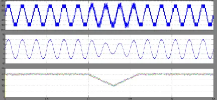
Fig. 7. Simulation results of NNPC inverter with SPWM and the voltage balancing method for ma =0.8 (t<0.1 s) and ma =0.5 (t>0.1 s). (a) Line–line voltage. (b) Phase current. (c) Six FC voltages
Fig. 4 illustrates the simulation results of the NNPC inverter with SPWM and the proposed voltage-balancing method.
Fig.8. Simulation results of NNPC inverter with SVM and the voltage balancing method for ma =0.8 (t<0.1 s) and ma =0.5 (t>0.1 s). (a) Line–line voltage.
(b) Phase current. (c) Six FC voltages. Fig. 5 shows the simulation results of NNPC inverter when SVM and the proposed voltage-balancing method are applied, with ma =0.8whent<0.1s, and ma =0.5whent>0.1s.
Dynamic processes of the FC voltages are also investigated and shown in Fig. 6 for SPWM scheme and in Fig. 7 for SVM scheme with the proposed voltage-balancing method.
Fig. 9. Simulation results of NNPC inverter with and without the capacitor voltage-balancing control under
Fig. 10. Simulation results of NNPC inverter with and without the capacitor voltage-balancing control under SVM scheme. (a) Line–line voltage. (b) Phase
current. (c) Six FC voltages.
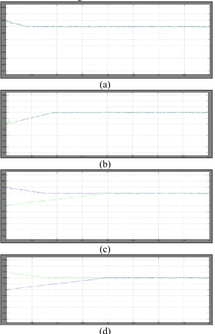
Four different initial capacitor voltage unbalances have been studied to verify the ability of the voltage-balancing method. The results with ma =0.8are shown in Fig. 11.
(a)
(b)
(c)
(d)
Fig. 11. Capacitor voltages ofVCa1 andVCa2 starting with different initial voltage unbalances (ma =0.8).
(a)VCa1 =VCa2 =Vdc/2.(b)VCa1 = VCa2 =0.(c)VCa1 =Vdc/2andVCa2 =0.(d)VCa1
=0andVCa2 = Vdc/2.
As previously analyzed, the two capacitors in a leg of the NNPC inverter are coupled. The coupling will bring some limitations to the inverter in some applications in terms of the capacitor size.
(a)
(b)
Fig. 12. FC value versus the inverter fundamental frequency with maximum peak-to-peak capacitor voltage ripple of 15%. (a) Fan/pump type of loads.
(b) Constant torque type of loads.
Under these conditions, the required capacitor sizes in per unit (p.u.) are given in Fig. 12(a) and (b) for fan/pump and constant torque types of loads, respectively.
CONCLUSION
motor and need not be synchronized, speed and accuracy, robust and sturdy and they can operate in a wide range of industrial conditions. The effectiveness and feasibility of the proposed method is determined by using the simulation results and also analyze the proposed method.
REFERENCES
[1] B. Wu, High-Power Converters and AC Drives.New York, NY, USA: Wiley/IEEE Press, 2006, ch. 1.
[2] N. Mittal, B. Singh, S. P. Singh, R. Dixit, and D. Kumar, “Multilevel inverters: A literature survey on topologies and control strategies,” in Proc. 2nd Int. Conf. Power, Control Embedded Syst., 2012, pp. 1–11. [3] J. Rodriguez, J.-S. Lai, and F. Z. Peng, “Multilevel inverters: A survey of topologies, controls, and applications,”IEEE Trans. Ind. Electron., vol. 49, no. 4, pp. 724–738, Aug. 2002.
[4] R. Stala, “A natural dc-link voltage balancing of diode-clamped inverters in parallel systems,”IEEE Trans. Ind. Electron., vol. 60, no. 11, pp. 5008– 5018, Nov. 2013.
[5] J. Mei, K. Shen, B. Xiao, L. M. Tolbert, and J. Zheng, “A new selective loop bias mapping phase disposition PWM with dynamic voltage balance capability for modular multilevel converter,”IEEE Trans. Ind. Electron., vol. 61, no. 2, pp. 798–807, Feb. 2014.
[6] M. Narimani, B. Wu, Z. Cheng, and N. Zargari, “A new nested neutral point clamped (NNPC) converter for medium-voltage (MV) power conversion,”IEEE Trans. Power Electron., vol. 29, no. 12, pp. 5259–5270, Dec. 2014.
[7] A. Choudhury, P. Pillay, and S. S. Williamson, “DC-link voltage balancing for a three-level electric vehicle traction inverter using an innovative switching sequence control scheme,”IEEE Trans. Emerg. Sel. Topics Power Electron., vol. 2, no. 2, pp. 296–307, Jun. 2014. [8] Z. Shu, N. Ding, J. Chen, H. Zhu, and X. He, “Multilevel SVPWM With dc-link capacitor voltage balancing control for diode-clamped multilevel converter based STATCOM,”IEEE
Trans. Ind. Electron., vol. 60, no. 5, pp. 1884– 1896, May 2013.
[9] S. Busquets-Monge, S. Alepuz, J. Bordonau, and J. Peracaula, “Voltage balancing control of diode-clamped multilevel converters with passive front-ends,”IEEE Trans. Power Electron., vol. 23, no. 4, pp. 1751–1758, Jul. 2008.
[10] S. Busquets-Monge, R. Maheshwari, and S. Munk-Nielsen, “Overmodulation of n-Level three-leg dc-ac diode-clamped converters with comprehensive capacitor voltage balance,”IEEE Trans. Ind. Electron., vol. 60, no. 5, pp. 1872– 1883, May 2013.
[11] A. H. Bhat and N. Langer, “Capacitor voltage balancing of three-phase neutral-point-clamped rectifier using modified reference vector, ”IEEE Trans. Power Electron., vol. 29, no. 2, pp. 561–568, Feb. 2014.
[12] J. Pou, R. Pindado, and D. Boroyevich, “Voltage-balance limits in four level diode-clamped converters with passive front ends, ”IEEE Trans. Ind. Electron., vol. 52, no. 1, pp. 190–196, Feb. 2005.
[13] P. Chaturvedi, S. Jain, and P. Agarwal, “Carrier-based neutral point potential regulator with reduced switching losses for three-level diode-clamped inverter,” IEEE Trans. Ind. Electron., vol. 61, no. 2, pp. 613–624, Feb. 2014.
[14] M. Khazraei, H. Sepahvand, K. Corzine, and M. Ferdowsi, “A generalized capacitor voltage balancing scheme for flying capacitor multilevel converters,” in Proc. 25th Annu. IEEE Appl. Power Electron. Conf. Expo., 2010, pp. 58–62.
BOORUGUPALLI VISHNU VARDHAN
Completed B.Tech in Electrical & Electronics Engineering in 2014 from BVRIT affiliated to JNTU,HYDERABAD and Pursuing M.Tech form ST.MARTIN’S ENGINEERING COLLEGE Affiliated to JNTUH, Hyderabad, Telangana, India. Area of interest includes Power Electronics.
E-mail id; [email protected]
DR. K. SHASHIDHAR REDDY
Completed B.Tech,M.Tech,Ph.D.Working as Professor and Head of the Department at St.Martin’s Enggineering college,Dhulapally,Near kompally,secunderabad, Telangana, India. Area of interest includes Electrical Power System ,power electronics, electrical drives control.