Available online: https://edupediapublications.org/journals/index.php/IJR/ P a g e | 2506
Design of Controller for Three-Phase Ups System Operating
Under Profoundly Nonlinear Loads.
T.Dinesh & Dr.T.Anil Kumar
1Assistant Professor, Anurag Group of Institutions(CVSR), Venkatapur(V), Ghatkesar(M). 2Professor, Anurag Group of Institutions(CVSR), Venkatapur(V), Ghatkesar(M).
ABSTRACT- This paper displays the configuration of a high-octane space-vector pulse width regulation (SVPWM) controller for three phase uninterruptible energy supply (UPS) frameworks that would operating under exceptionally nonlinear loads. The established SVPWM method is truly viable for controlling those RMS extent of the UPS output voltages. However, it is not adequate on compensating the harmonics and the distortions created particularly by the nonlinear currents drawn toward those rectifier loads. The distortion becomes more severe at high power where the switching frequency has to be reduced due to the efficiency concerns. This study proposes a new design strategy that overcomes the limitations of the classical RMS control. It includes internal loops of the closed-loop control system effectively that empowers effective decrease from harmonics also compensation of distortion toward the outputs. Simulink is used to analyze, develop, and design the controller using the state-space model of the inverter. Those controller will be executed in the execution is assessed tentatively utilizing a three-phase 10 kVA transformer separated UPS under the sum sorts about load states. Previously, conclusion, the test Outcomes indicate that the controller successfully accomplishes those steady-state RMS voltage regulation determinations and in addition the total harmonic distortion and the dynamic response requirements of real UPS principles.
Index Terms—Inverter, nonlinear load ,space vector pulse width modulation (SVPWM), control uninterruptible power supply (UPS).
I. INTRODUCTION
The increased use of rectifiers in critical loads employed by the information technologies, and medical and military equipment mandate the design of uninterruptible power supplies(UPS) with high-quality outputs [1]–[3]. The highly non linear currents drawn especially by high-power single-phase rectifier loads greatly distort the UPS outputs. The distorted UPS voltages cause generation of low dc voltage at the output of the rectifier loads, which causes high current flow, increased power losses, and possibly the malfunction of the critical load or the UPS.
The distortion is resulted mainly by the voltage drop across the inductive element of the LC filter due to the no sinusoidal current at the output of the inverter [4]–[6]. In a UPS system, the inverter is
responsible for synthesizing sinusoidal voltages from a dc source through the pulse width modulation (PWM) of the dc voltage. The inductive element here is needed to remove the switching frequency harmonics from the current waveform that are generated by the PWM operation of the inverter. The inductance value can be reduced if the switching frequency is increased. But, in practice, it has an upper limit at high power inverters due to the efficiency concerns and the switching device limitations. So, for the selected switching frequency and the power level, an optimum filter with a smallest inductance can be designed, but the distortion cannot be completely avoided, and the regulations and the customer specifications may not be satisfied.
The solution to this problem is to design a proper inverter controller such that it generates a control signal with multiple functionalities. This sign must convey majority of the data to process sinusoidal voltages for little steady-state RMS error, should furnish quick transient reaction and restorative activities to decrease distortion actually under profoundly nonlinear loads. Therefore, a major look into need been directed with plan such controllers for those high-octane UPS frameworks [2]–[5], those secondary execution controllers as a rule utilized multi loop state feedback control methodologies with attain those regulation specifications[9].
The dead-beat control method and the predictive and repetitive control methods have been widely investigated and proposed among researchers. In addition, the iterative and adaptive learning control methods, the H-infinity control method the feedback linearization method, and recently the multi sampled control approach to improve the control performance have been studied and evaluated.
(SVPWM)-Available online: https://edupediapublications.org/journals/index.php/IJR/ P a g e | 2507
based controllers are the primary choice of many researchers and the applications currently used in industry. However, the classical sinusoidal PWM (SPWM) method is still preferred by many manufacturers because of its implementation simplicity, easy tuning even under load, flexibility, and most importantly the advantages of controlling each phase independently. The independent regulation of each phase provides easy balancing of three-phase voltages which makes heavily unbalanced loading possible. Also, it avoids problems such as transformer saturation. Although the classical SPWM method is quite effective in controlling the RMS magnitude of the UPS output voltages, it is not good enough in compensating the harmonics and the distortion caused specifically by the nonlinear loads For example, the total harmonic distortion (THD) is greater than 5% limit even with good filtering. It becomes more severe at high-power UPSs where the switching frequency has to be reduced due to the efficiency and heating problems.
This study proposes a multiloop high-performance SPWM control strategy and a design that overcome the limitations of the classical RMS control. It adds inner loops to the closed loop feedback control system effectively that enables successful reduction of harmonics and compensation of distortion at the voltages. The experimental setup using the proposed controller achieves 3.8% THD under the nonlinear load having a crest factor of 3 and absorbing power equal to the rated power of the UPS. Recently, the proportional plus resonant (PR) controller has gained popularity because of its simple structure and high performance. The PR controller method basically provides a high gain only at the desired frequencies (mostly at the fundamental frequency of an input or an output) and therefore very effective in correcting the steady-state error and obtaining a good tracking of the reference at the reference frequency.
According to the recent literature, it is a very popular control method for grid tied inverters and PFC rectifiers where the current is controlled in such a way that it tracks the grid voltage for high power quality. Because of its popularity, we evaluated the method for our UPS application. According to our simulation studies, the proposed multi loop controller performs better than the PR controller and achieves 20% less THD. However, when the PR controller is combined into the proposed controller, the result changes in the favor of the combined controller and it achieves 2.5% THD. The details of the controller and some simulation results are given in Section VII.
One limitation of the PR method is the possible shifting of frequencies caused by the calculation errors when digitally implemented. For example, if 50 Hz or other harmonic components change frequency, the controller coefficients may need to be recalculated. And online calculation is not practical. In addition ,the gain at the desired frequency may go to infinity. Therefore, a filter that has a little wider bandwidth must be designed. This reduces the gain. But, then there might be an interference of other frequencies.
The harmonic droop method is another technique that has appeared also recently Power at each frequency. Therefore, the switching frequency is limited to a low level. In, the authors state, ―The deciding criterion when selecting the appropriate control scheme usually involves an optimal trade off between cost, complexity and waveform quality needed for meeting waveform quality standards.
In other words, if you believe that the controller you selected for your application satisfies the waveform quality requirements, then you would naturally look for the one that is the lowest in cost and the simplest one so that your implementation effort is reduced. In practice, the low cost and simplicity contribute to a product that is very competitive in the market. As far as the steady-state regulations, the THD, and the dynamic response performances, the proposed method yields similar results compared to the other classical methods, and successfully satisfies the waveform quality requirements of the major UPS standards.
The proposed controller does not seem to have a prominent significance over the others. However, the significance of the proposed multiloop controller compared to other methods is as follows:
1)The execution time is less and allows higher switching frequencies. The complex control algorithms take longer execution times and may limit the upper boundary of the switching frequency where you have actually some allowance for higher switching frequency operation. Examples to the complex controllers are the repetitive, predictive, and harmonic droop controllers.
2) The cost is low. Some control algorithms require
Available online: https://edupediapublications.org/journals/index.php/IJR/ P a g e | 2508
3) The easy tuning even under load: Some are robust to this kind of tuning and some may not. This feature is preferred by some manufacturers. The easy tuning of the proposed method under load is verified during the experimental studies.
4) The flexibility: It means that you can modify your controller and optimize it according to the customer specifications at the time of installation or later in use. The optimization may include obtaining the lowest THD or the best tracking of the RMS value or the fastest dynamic response. So, the controller should be flexible any Tim Do any of the aforementioned optimizations without significantly affecting the others. We have also verified this feature experimentally.
5) The scalability: It means that the controller is easy to design and tunable for any power level.
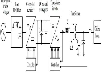
II. SYSTEM DESCRIPTION
The single-line diagram of a typical three-phase four-wire transformer isolated UPS system is given in Fig. 1.
Fig. 1. Single-line diagram of a typical three-phase four-wire transformer isolated UPS system.
The three phase thyristor-based controlled rectifier converts the mains voltages into a constant dc and also provides standalone charge to the batteries. Then, a six-switch PWM voltage source inverter(VSI) creates balanced three-phase sinusoidal voltages across the load terminals at the utilization frequency and magnitude. The LC low-pass filter removes the harmonics generated by the PWM switching. The Δ-winding of the transformer blocks the third harmonic currents at the inverter side, and the zigzag winding provides a neutral point and zero phase difference for the load-side voltages. The load can be a three-phase or a single phase load ranging from linear to nonlinear load with a crest factor up to 3. The UPS uses a digital controller implemented in a fixed-point DSP controller.
III. ANALYSIS OF THE UPS INVERTER POWER STAGE
This segment obtains those state-space model of the inverter stage of a three-phase UPS so as should outline those controller for the inverter. Those produced model is likewise utilized to study the controller performance to those most reduced THD of the output voltage while maintaining the stability and a good dynamic response under all load conditions. The model is developed based on the circuit schematic given in Fig. 2. As shown in Fig. 2, an insulated gate bipolar transistor (IGBT)-based three-phase inverter is used to produce pulse-width modulated voltages across the terminals labeled as 1, 2, and 3. Moreover, L is the external filter inductor used to reduce ripple at the line current, Llk1 is the primary side leakage, and Lμ is the magnetizing inductance of the transformer; then Llk2 is the secondary side leakage inductance, C_is the filter capacitor, and finally R_ is the load resistance (the prime symbol represents the parameters referred to the Δ-side of the transformer).
Writing the voltage equations at the Δ-side of the transformer yields the following sets of equations for the line-to-line voltages across the inverter terminals, (1) as shown at the bottom of the page. Similarly, writing the current equations yields the following sets of equations for the derivative of the transformer secondary currents:
Fig. 2. UPS inverter stage including the Δ-zigzag transformer equivalent circuit and the resistive load.
Likewise, the following sets of equations are obtained for the derivative of the referred output voltages based on the output parameters.
IV. DESIGN OF THE INVERTER POWER STAGE
Available online: https://edupediapublications.org/journals/index.php/IJR/ P a g e | 2509
classical methods and the rule of thumbs suggested in the power electronics literature. However, this design did not give a good performance under nonlinear loads. Then, it is improved via simulation studies until the desired performance is achieved for all load cases. The improvements included determination of the proper dc bus voltage, switching frequency, transformer parameters, and the element values of the
LC filter.
Our preliminary design goal is to maintain the THD always below 4% under the worst case. The worst case is defined as the instant dc bus voltage is at the minimum while the UPS is delivering the rated nonlinear load. For that reason, selecting the nominal modulation ratio around 0.7 is considered optimum since it guarantees the linear PWM operation under the worst case. The simulation studies have shown that if the controller goes into over modulation region, the THD specification cannot be satisfied. Therefore, the nominal dc bus voltage is maintained at 405 V when grid is okay and it is allowed to reduce down to300 V when grid is gone and the UPS operates from the battery pack. One string of the battery pack consists of 30 pieces of12 V lead-acid batteries connected in series. Thus, the controller achieves 3.54% THD at the worst case where the modulation ratio is almost 1.0.
The switching frequency is selected as 10.05 KHz. The inverter uses CM100DU-12F Power ex IGBTs that allow reliable operation at the selected frequency. A 10 kVA,√3 ×(170/220)V, Δ-zigzag connected transformer having a total series leakage reactance of 3.33%, which corresponds to 920 μH, is used for galvanic isolation and step-up purposes. Based on the results of the previous research, as presented in [4]–[6], and based on our simulation studies, it has been realized that the output impedance of an inverter plays an important role in reducing the THD of the output voltage. And the results show that the THD of the voltage can be improved if the output impedance is reduced [5] or the impedance is modified to become even more capacitive in nature [6]. Our approach to design the LC filter is to start first with finding practically the smallest inductance value, and then finding the capacitance value based on filtering requirement of the switching frequency ripple at the output voltage.
Generally, the inductance is selected based on the current ripple, size, and dynamic response criteria. Since we want the smallest inductance, we base our inductor design on the ripple requirement. The current through the inductor also flows through the IGBTs of the three-phase inverter at every
switching Cycle. So, based on our experience, allowing 30% ripple at the current is considered a good compromise between the size and the efficiency requirements. More than 30% ripple allows smaller inductance but causes larger turn-off switching losses. Hence, the inductance is calculated based on the aforementioned ripple specification, and then the capacitance value is calculated in such a way that the
LC filter produces 30 dB attenuation at the switching frequency. So, using the aforementioned criteria, the filter inductance is found as 1010 μH at the inverter side and the capacitor is 120 μF placed at the load side. The calculated inductance yields around 30% current ripple at the inverter line currents at the full linear load and a corner frequency of 352 Hz for the
LC filter. As shown in Fig. 3, an external inductor equal.
Fig. 3.Mat lab model of the designed inverter power stage including delta–zigzag transformer, the
LC filter, the measurements, and the linear and nonlinear loads. to 30μH is added at each line to arrive at the required filter inductance value.
Available online: https://edupediapublications.org/journals/index.php/IJR/ P a g e | 2510
since the specification of products requested by many customers today require the UPS to handle loads up to 3 crest factor while allowing a THD no more than 5%.
Finally, the schematic of the inverter with the parameter values optimized for all load conditions is shown in Fig. 3.The inverter circuit is modeled in the piecewise linear electrical circuit simulation (PLECS) which is a Simulink tool box for system-level simulations of electrical circuits developed by
V. STATE-SPACE MODEL OF THE INVERTER POWER STAGE
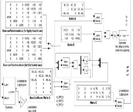
The state-space model of the plant (three-phase inverter)is needed to develop and test the controller performance. So, using L = 30 μH, Lμ= 1 H, Llk1 820
μH, L_lk2 =100 μH, C_ = 202 μF, Vdc = 405 V,Vtri = 2487, R_ = 10 Ω for full load and R_ = 255 Ω for the light load case in (5)through (13), the state-space model of the plant is obtained as shown in Fig. 4.
Fig. 4. State-space model of the inverter power stage (the plant) including the closed-loop control system
and the controller built in Simulink
The peak of the carrier waveform is obtained based on the type of the selected DSP and the switching frequency. The details of the controller are discussed in the next section.
VI. CONTROLLER DESIGN
This section presents the design of the proposed inverter controller. The controller is based on the multiloop SPWM method as shown in Fig. 5, which is also shown as a block in Fig. 4. The controller topology is very similar to the classical state-feedback multiloop controllers [8], [9], except that all the loops are combined(instead of cascade connection) before they are applied to the PWM generator. This feature basically adds the relative benefits of each loop and creates a more effective
multiloop strategy. In order to facilitate the understanding of the proposed Controller, the reasoning behind the selected control topology can be explained as follows.
Fig. 5. Simulink model of the proposed multiloop controller
The control system shown in Fig. 5 consists of one outer voltage loop and three inner loops. The outer loop is the main voltage loop, which regulates the fundamental Frequency component of the output voltage and its steady-state RMS value using a PI compensator; for that reason, it has slower dynamics.
The first of the inner loops is the voltage reference feed forward loop which provides fast transient response but less benefit to the compensation of the harmonic distortions. The second inner loop is the voltage loop where the measured ac output voltages are instantaneously compared to the reference ac voltages created by the main loop and the error (Error1) is found; then the loop is compensated using a PD controller. This loop is responsible for correcting the phase shift and improving the waveform quality of the output voltages. The simulation results confirm that the gain Kp2 controls the THD of the voltages effectively and improves the waveform quality. The
Available online: https://edupediapublications.org/journals/index.php/IJR/ P a g e | 2511
In this loop, the measured inductor currents are instantaneously compared to the reference currents created by the main loop and the resulted error (Error2) is combined to the main control output after it is multiplied by the gain Kp3, as shown in Fig. 5.Our studies have shown that the ac current loop with the gainKp3 stabilizes the control system effectively..The advantage of the multiloop control system proposed here is that the loops can be optimized for the best performance relatively independent of each other. For example, the outer voltage loop is tuned first for the best voltage regulation, and then the inner loops can be optimized. Best THD of the output voltage while effectively managing and maintaining the stability.
The design and the analysis of the proposed controller have been done using the Simulink Control Design Linear Analysis tool which performs linearization and steady-state operating point analysis of a model built in the Simulink, and also generates various small-signal plots including Bode, step response, Impulse response, pole/zero, Nyquist, and so on. To use this tool, we need to select linearization input and output points in the Simulink model. As shown in Fig. 4, one input and two output points are placed to determine the loop gain and to analyze the dynamics of the main control loop and the dynamics from the control to the output.
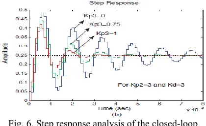
The controller parameters are determined as follows. Based on the steady-state voltage regulation and transient response specifications given in Table I, first the gains of the main voltage loop are determined as Kp1 = 2 and Ki = 0.05, as shown in Fig. 5. Then, the Kp2 = 3 is determined for the practical lowest THD while Kd and Kp3 are adjusted to maintain a stable operation. The proper gains for Kd and Kp3 are obtained using the control design tool for the lightly loaded case in the model shown in Fig. 4. The lightly loaded case is the worst casein terms of the stability.
Fig. 6. Step response analysis of the closed-loop control system: (a) for Kp2= 3, Kd = 0, and Kp3 = 0;
(b) for Kp2 = 3, Kd = 3, Kp3 = 0 (blue), Kp3 =0.75 (green), and Kp3 = 1.0 (red).
Fig. 6 shows the results of the step response analysis and also illustrates the steps of the process show the controller parameters are determined. When only the ac inner voltage loop is active, that is, Kp2 = 3, Kd = 0, andKp3 = 0, as mentioned before, the system is unstable as seen in Fig. 6(a). On the other hand, the derivative control whereKp2 = 3, Kd = 3, and Kp3 = 0 stabilizes the system, but not very effectively [the blue waveform in Fig. 6(b)]. However, amore effective stable operation is obtained when the third loop(the inner ac current loop) is activated. Fig. 6(b) shows the results for Kp2 = 3, Kd = 3, and Kp3 = 0.75 as the green wave form, and for Kp2 = 3, Kd = 3, and Kp3 = 1 as the red waveform.
Fig. 7.Simulink model of the inverter system. Consequently, Fig. 7 shows the complete control system schematic implemented in the Texas Instrument’s signed 32-bit fixed-point IQ numbers with fraction length set to10 for all calculations.
Available online: https://edupediapublications.org/journals/index.php/IJR/ P a g e | 2512
VII. SIMULATION RESULTS A. Proposed Multiloop Controller
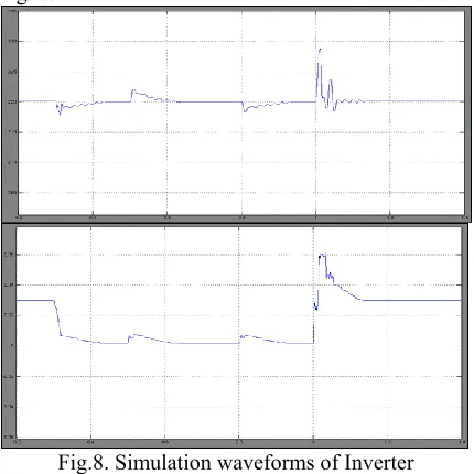
The simulations are done in the MATLAB/Simulink environment using the Simulink model of the inverter and the waveform as shown in Fig. 8.
Fig.8. Simulation waveforms of Inverter The results are evaluated based on steady-state error, transient response, and the THD of the output voltage. Fig. 9 shows the RMS value and the percent THD of the output voltage versus three different loads.
Fig. 9.RMS fluctuations (top trace) and the profile of the percent THD of the output voltages (second trace)
versus the load delivered by the inverter (bottom trace).
According to Fig. 9, when the linear load at 8.5 kW is applied, the controller achieves 0.3% THD, and similarly when the nonlinear load at 10kVA is applied, the controller achieves 3.1% THD. In addition, the RMS voltages are very well regulated at 220 V for each phase with an excellent transient response for the linear load but a fair response for the nonlinear load case. The transient response from
no-load to the rated nonlinear no-load is oscillatory and it takes 1.1 s; however, the maximum fluctuation in the RMS voltage is less than 10% of the nominal (198– 242 V).We consider this as an expected behavior for the nonlinear load case since the capacitor of the rectifier is made fairly large to get the desired crest in current; additionally, it is all empty before the load is applied. At the instant, the rectifier loads are switched in, a very large inrush current flows into these capacitors. So, it is this current that causes the oscillatory behavior. As mentioned before, the nonlinear load is a full-bridge diode rectifier load..
The simulated load consists of a light load, the linear full load, and the nonlinear full load placed between each phase and the neutral as shown in Fig. 3.In conclusion, the simulation results demonstrate the effectiveness of the proposed multiloop controller system and also verify the design.
B. Comparison of the Proposed Controller and the PR Controller
In order to judge the performance of the proposed controller, we selected the PR controller as the bench mark and compared the results of each. The PR controller has gained very good popularity in many inverter applications especially where an excellent reference tracking is desired.
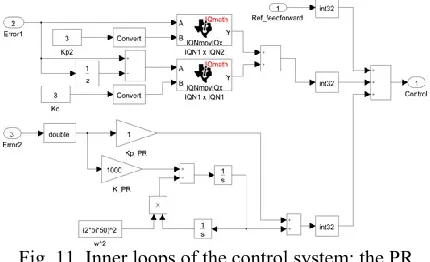
Fig. 10 shows the details of the inner loops of the control system for the PR controlled UPS. Note that the controller includes a derivative controller that compensates Error1. Without the derivative, the PR controller alone achieves a THD of 4.65%, and with the derivative the THD becomes 3.88%.
Fig. 10. Inner loops of the control system: the PR controller is combined with the derivative controller
Available online: https://edupediapublications.org/journals/index.php/IJR/ P a g e | 2513
combined into the proposed controller as shown in Fig. 11.
Fig. 11. Inner loops of the control system: the PR controller is combined into
The result changes in the favor of the combined controller and it achieves 2.5% THD. The results confirm two points: our multiloop strategy is good for this application and the PR controller performs very well within a multiloop strategy. However, according to the reasons that are discussed in Section I, the proposed method is preferred and implemented for this UPS application.
VIII. SIMULATION RESULTS
A UPS system rated at 10 kVA, 50 Hz, 380 V was built and tested to evaluate the performance of the controller and the design. The implemented system uses the component values given in the PLECS simulation model of the converter shown in Fig. 3(in Section IV) for the inverter part and the values given in Fig. 7(in Section VI) for the controller part.
In Fig. 12, we compare the results of the multiloop design against the single-loop (only the RMS control) design in order to demonstrate the performance of the proposed multiloop controller.
Fig. 12. Upper trace is the profile of the %THD of the output voltage of one phase measured for three different loading conditions. The lower trace is the
total output apparent power delivered by the UPS into these loads.
Fig. 12 compares the measured three-phase output voltages and the current of one phase for two loading conditions: the linear full load and the nonlinear full load. Fig. 12(a) and (b) show the results when only the RMS control is used (single-loop), for this case the control achieves 1.96% THD for the linear and 9.68% THD for the nonlinear load. It is clear that the RMS control alone cannot achieve an acceptable THD under nonlinear loading at the rated UPS output power. The waveforms in Fig. 12(c) and (d) show the results when the proposed multiloop controller is used for the same loading conditions. In this case, the controller achieves1.11% THD for the linear load and 3.8% THD for the nonlinear load. The crest factor of the current in Fig. 12(d) is measured as2.8.
The THD measurements given previously and also shown in Fig. 13 were taken by the 3196 HIOKI power quality analyzer. The upper trace in Fig. 13 shows the profile of the %THD of the output voltage of one phase versus the three different loading conditions: nonlinear full load, linear full load, and no load.
Fig.13. Measured transient response of output voltages (upper trace) and currents (lower trace) when the load changes from no load to the full linear
load. The scale of the vertical axis of upper trace is 100 V/div, and the lower trace is 25 A/div. The scale
of the horizontal axis is 2 cycle/div.
The lower trace shows the total output apparent power delivered into these loads. The test was set up to supply each load approximately over a one-min interval.
As shown in the lower trace of Fig. 13, the UPS was initially loaded with the rated single-phase rectifier load, then no load, 1 min later a resistive load at 8.5 kW, and finally the same rectifier load is applied again.
Available online: https://edupediapublications.org/journals/index.php/IJR/ P a g e | 2514
follow the simulation results except a minor (0.7%) increase in the overall THD readings. But, it is also clear from Fig. 13 that this increase is measured for all load conditions. And it is not specific to the nonlinear case only. So, in brief, the implications are that this overall increase is due to the unpredicted parasitic effects.
Fig.14 Dynamic response waveforms using simulink The dynamic response simulation results are presented in Figs. 14. Fig. 14(a) shows the records of events occurred when the linear full load is switched in and out, and Fig. 14(b) shows the events when the nonlinear load is switched in. According to these results, the transient voltage magnitude regulation for linear loads is less.
Fig. 15. Measured transient response of the output voltages (upper trace) and the currents (lower trace)
when the load changes from no load to the rated single-phase rectifier load placed at each phase. The scale of the vertical axis of upper trace is 100 V/div, and the lower trace is 25 A/div. The scale of the
horizontal axis is 2 cycle/div.
The measured transient response of output voltages and currents when the load changes from no load to the full linear load is given in Fig. 15.
IX. CONCLUSION
This paper presents the analysis and design of a higher performance SVPWM controller for three-phase UPS systems powering highly nonlinear loads. Although the classical SVPWM method is very successful in controlling the RMS magnitude of the UPS output voltages, it cannot effectively compensate for the harmonics and the distortion caused by the nonlinear currents drawn by the rectifier loads. Therefore, this paper proposes a new strategy with a new design that overcomes the limitations of the classical RMS control. It adds inner loops to the closed loop control system effectively that enables successful reduction of harmonics and compensation of distortion at the voltages. The controller performance is evaluated experimentally using a three-phase 10 kVA transformer isolated UPS. A THD equal to 3.8% at the output voltage is achieved even under the worst nonlinear load. The load consists of three single-phase rectifiers connected between each line and the neutral and absorbing power equal to the rated power of the UPS with a crest factor up to 3. In conclusion, the experimental results demonstrate that the proposed controller successfully achieves the steady-state RMS voltage regulation specification as well as the THD and the dynamic response requirements of major UPS standards.
REFERENCES
[1] Uninterruptible power systems (UPS)—Part 3: Method of specifying the performance and test requirements, First Edition 1999-03, International Standard IEC 62040-3.
[2] F. Botter´on and H. Pinheiro, ―A three-phase UPS that complies with the standard IEC 62040-3,‖ IEEE Trans. Ind. Electron., vol. 54, no. 4,pp. 2120–2136, Aug. 2007.
three-Available online: https://edupediapublications.org/journals/index.php/IJR/ P a g e | 2515
phase UPS inverters,‖ IEEE Trans. Power Electron., vol. 27, no. 6, pp. 2294–3005, 2012.
[4] U. Borup, P. N. Enjeti, and F. Blaabjerg, ―A new space-vector-based controlmethod for UPS systems powering nonlinear and unbalanced loads,‖IEEE Trans. Industry Appl., vol. 37, no. 6, pp. 1864–1870, Nov./Dec.2001.
[5] Q.-C. Zhong, F. Blaabjerg, J. Guerrero, and T. Hornik, ―Reduction ofvoltage harmonics for parallel-operated inverters equipped with a robust droop controller,‖ in Proc. IEEE Energy Convers. Congr. Expo., Phoenix,AZ, 2011, pp. 473–478.
[6] Q.-C. Zhong and Y. Zing, ―Can the output impedance of an inverter bedesigned capacitive?‖ in Proc. 37th Ann. IEEE Conf. Ind. Electron., 2011,pp. 1220–1225.
[7] P.Mattavelli, ―Synchronous-frame harmonic control for high-performanceAC power supplies,‖ IEEE Trans. Ind. Appl., vol. 37, no. 3, pp. 864– 872,May/Jun. 2001.
[8] N. M. Abdel-Rahim and J. E. Quaicoe, ―Analysis and design of a multiplefeedback loop control strategy for single-phase voltage-source UPS inverters,‖ IEEE Trans. Power Electron., vol. 11, no. 4, pp. 532–541, Jul.1996.